AMAZON multi-meters discounts AMAZON oscilloscope discounts
...
6. Output Blocks
In general the output section of any switching power supply is comprised of single or multiple DC voltages, which are derived by direct rectification and filtering of the transformer secondary voltages and in some cases further filtering by additional series ‑ pass regulators or LDOs. These outputs are normally low voltage, direct current, and capable of delivering a certain power level to drive electronic components and circuits. The most common output DC voltages are 3.3 V, 5 V, ±12 V, 2.5 V, 1.8 V, 1.2 V, etc., and their power capability may vary from a few watts to thousands of watts. The most common type of secondary voltages that have to be rectified in a switching power supply are high ‑ frequency square waves. These, in turn, require special components, such as Schottky diodes or fast-recovery rectifiers, low-ESR capacitors, and energy storage inductors, in order to produce low noise outputs useful to the majority of electronic components.
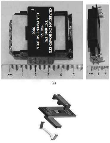
FIG. 11 Integrated PC board planar transformer.
6.1 Output Rectification and Filtering Schemes
The output rectification and filtering scheme used in a power supply depends on the type of supply topology the designer chooses to use. The conventional flyback converter uses the output scheme shown in FIG. 12(a). Since the transformer T1 in the flyback converter also acts as an energy-storing inductor, diode D1 and capacitor C1 are the only two elements necessary to produce a DC output. Some practical designs, however, may require.
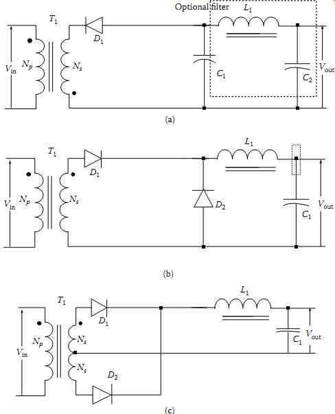
FIG. 12 Output stages: (a) flyback type; (b) forward type; (c) push-pull/half-Bridge/full-bridge.
the optional insertion of an additional LC filter, shown in FIG. 12(a), to suppress high ‑ frequency switching spikes. The physical and electrical values of both L1 and C2 will be small. For the flyback converter, the rectifier diode D1 must have a reverse-voltage rating of (1.2 Vin (NS /NP)), minimum.
The output section of a forward converter is shown in FIG. 12(b). Notice the distinct differences in the scheme compared to the flyback. Here, an extra diode D2 called the flywheel is added, and also inductor L1 precedes the smoothing capacitor. Diode D2 provides current to the output during the off period. Therefore the combination of diodes D1 and D2 must be capable of delivering full output current, while their reverse blocking voltage capabilities will be equal to (1.2Vin (Ns/Np)), minimum.
The output section that is shown in FIG. 12(c) is used for push - pull, half - bridge, and full - bridge converters. Since each of the two diodes D1 and D2 provides current to the output for approximately half of the cycle, they share the load current equally.
An interesting point is that no flywheel diode is needed, because either diode acts as a flywheel when the other one is turned off. Either diode must have a reverse-blocking capability of (2.4 Vout (Vin,max/Vin,min)), minimum.
6.2 Post-regulation Techniques
In many common processor-based load environments, the load may require very tightly regulated outputs together with excellent transient response at the power supply output for fast-changing load currents. The output ripple of transformer-isolated multiple-rail DC-DC converters is typically between 0.5% and 1% of the nominal output, whereas a linear regulator can perform within a millivolt- or even a microvolt order ripple. The transient response of a 50%-100% (or vice versa) load step can range from 100 to 300 μs for an isolated DC-DC converter, whereas a linear supply can respond within 1-5 μs for a similar load current step. In demanding situations of loads where tight regulation and fast transient response are required, post-regulation techniques can be used. This is particularly the case when multiple voltage rails are available in a power supply system. The basic principle behind all postregulation techniques is to use some extra regulator circuits at the output side of the switching power supply.
Some of the popular postregulation techniques include linear regulators, added secondary-side DC-DC converters, coupled inductors, magnetic amplifiers (mag amps; sometimes called saturable reactors), and secondary-side post-regulators (SSPRs).
FIG. 13 shows these concepts. A linear regulator block used as a secondary-side controller ( FIG. 13(a)) or a post-regulator is quite common and provides excellent transient response and minimum ripple.
However, for efficiency reasons these linear regulators should be in the form of LDOs.
Adding a second-stage DC-DC converter ( FIG. 13(b)) seems simple but can present design difficulties. Coupled inductors ( FIG. 13(c)) are suitable for secondary-rail situations, where lower regulation is acceptable, in a typical tolerance range of ±5%-±8%.
Tight coupling can create unwanted interactions between coupled outputs. Magnetic amplifier techniques are based on a saturable reactor, which can act as a magnetic switch ( FIG. 13(d)), exhibiting high or low impedance toward the output rail to be controlled.
Magnetic amplifiers are used for medium and high power requirements. The SSPR technique ( FIG. 13(e)) uses a semiconductor device as a switch, with a switchmode controller that is synchronized with the main PWM controller. Regulation of the voltage is achieved on the secondary side either by controlling the volt-second product across the output inductor for buck-derived techniques or by controlling the amount of energy for boost and flyback-derived topologies.
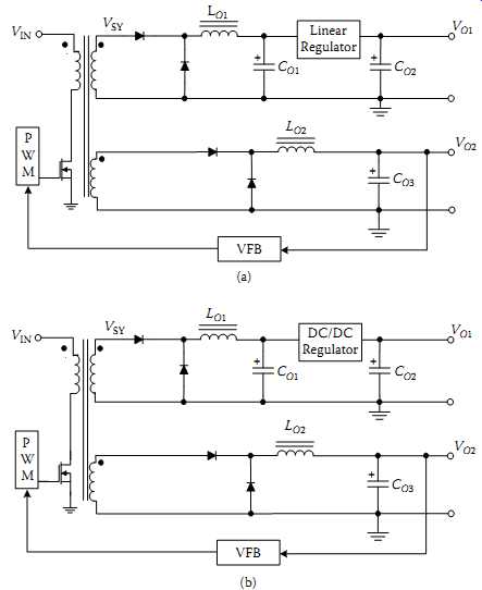
FIG. 13 Postregulation techniques: (a) linear regulator based; (b) switch-mode
controller based; (c) coupled inductor based; (d) magnetic amplifier based;
(e) secondary-side post-regulator (SSPR) based.
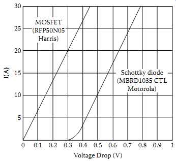
FIG. 14 Voltage drop of a MOSFET compared with a Schottky diode.
7. Efficiency Improvements and Synchronous Rectification
In Section 2, we briefly discussed the losses associated with a switching power supply.
In improving the efficiency of a power supply, every item must be carefully evaluated and optimized. In low-output voltage switching power supplies, losses in the output rectifiers and the switching losses in the transistors contribute a significant share. High frequency rectifiers usable in the output stage may be of three types: high-efficiency fast-recovery types, high-efficiency very fast rectifiers, and Schottky barrier rectifiers. A discussion of these can be found in (11). Recently, gallium arsenide (GaAs) and silicon carbide (SiC) devices have been introduced, and some of these could help improve the efficiency of the design.
For the lower DC rail voltage requirements, such as 1.2-3.3 V, of high-performance digital circuits, the high-efficiency requirement comes at very low-output voltages, and the general design approach using a Schottky diode becomes inadequate. In such circumstances, synchronous rectifiers (SRs) con figured using low-RDS(on) power MOSFETs can provide much better efficiencies. In all switching topologies, the output rectifiers can be conceptually replaced by power MOSFETs. This basically replaces the DC loss component because of the combination forward voltage (VFIRMS) and the I 2 rms rD (the resistive loss component in the diode) by a single element (I 2 rms RDS (on) of the MOSFET), providing significant efficiency improvements. FIG. 14 indicates a comparison of a typical Schottky diode and a MOSFET usable in an SR.
There are two basic types of SRs: self-driven (SDSR) and control-driven (CDSR).
FIG. 15 shows these types, and TBL. 2 compares their advantages and disadvantages.
More design details can be found in How (35). There are many controllers suitable for SR systems, and details on these advanced techniques.
In off-the-line SMPS similar to the silver box in PCs, there is much room for efficiency improvement. Easily identifiable areas of improvement can be classified into three major categories:
• An appropriate harmonic reduction front end with active PFC
• Architectural-level improvements to eliminate losses
• Component-level improvements and upgrades to reduce losses More detailed discussion and guidelines can be found in Dalal (42). Another important design consideration is the reduction of startup current-related losses (43). Another aspect is to reduce the losses due to stray and leakage inductances (44). Current-sensing resistors in switchers can also add significant losses. In situations where an inductor current is to be sensed, there are special techniques using a parallel RC network to sense the inductor current and minimize the loss across the series resistor inserted with the inductor (45).
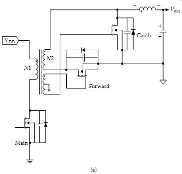
FIG. 15 Different types of synchronous rectifiers: (a) self-driven SR (SDSR);
(b) control driven SR (CDSR).
===
TBL. 2 Comparison of Synchronous Rectification Techniques
Technique Advantages Disadvantages Self-driven SR (SDSR) Simple For most topologies, drive signal amplitude varies with the line voltage When driven by transformer windings, there is no gate-driving voltage during dead time Problems when parallel operated Control-driven SR (CDSR) Constant gate signal, irrespective of line voltage and load changes Constant RDs(on)
Suitable for wide input voltage ranges Applicable for all topologies Dead time can be kept to a minimum Complex circuitry Needs accurate timing to prevent cross conduction
===
8. EMI Reduction
Because of high-frequency nonsinusoidal waveforms within the circuitry, a switching power supply generates noise that can emerge through conduction or radiation.
This noise can be conducted into the load or input source, and radiated components can create annoying situations in portable products such as cellular phones, PDAs, and laptops. U.S. and international standards for EMI-RFI have been established that require manufacturers to minimize the radiated and conducted interference of their equipment to acceptable levels. In the United States , the guiding document is FCC Docket 20780, and internationally the West German VDE- 08XX series is a well-accepted example. These standards generally exclude subassemblies from compliance, but the overall system should strictly adhere to the specifications. The main sources of high-frequency noise are the switching transistors, input and output rectifier stages, protective diodes, and the control ICs. The RFI noise level can vary with the topology used. Flyback converters, because of their near-triangular input current waveforms, generate less conducted RFI than topologies with rectangular input current waveforms.
EMI noise reduction is generally accomplished by three means: suppression of the noise source, isolation of the noise coupling path, and filtering and shielding.
Some advanced techniques are frequency modulation techniques and slew rate control.
Because the total spectrum of high frequencies should be minimized, measurement of conducted EMI noise using a spectrum analyzer is generally carried out, with adequate attention to the resolution bandwidth (RBW) of the spectrum analyzer or a similar test setup (46).
FIG. 16 Input line filters for SMPS systems: (a) basic version (b) an improved
version with two filter chokes.
The most common method of conducted noise suppression at the input of an off-line SMPS is the utilization of an LC filter for differential-mode and common-mode RFI suppression. Normally, a coupled inductor is inserted in series with each of the AC input lines, and capacitors are placed between lines (X capacitors) as well as between the lines and the earth terminal (Y capacitors). FIG. 16 indicates different line filter schemes used. The resistor R is for the discharge of the X capacitors, and the values are recommended by the relevant safety specifications under the VDE or IEC series.
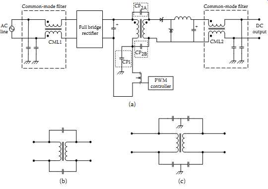
FIG. 17 A simplified example of a typical power supply with common mode
filters: (a) a general case indicating parasitic capacitances (b) parasitic
capacitances across a winding without a Faraday shield (c) Faraday shield
reducing the stray capacitance coupling.
Proper component layout and selection are important in controlling EMI. In a typical off-line power supply with common mode filters, the main source of common mode noise is the MOSFET. With the requirement of a heat sink, For example, in the case of a TO-220 package, the capacitance formed between the drain and the ground plane (CP1) in FIG. 17(a)) can conduct some common mode noise. In a typical power supply, such as in FIG. 17, the transformer can also conduct some high-frequency current through the parasitic capacitances formed between the windings. One technique to reduce the effects of these capacitances, such as CP2A and CP2B, is to use a Faraday shield for the windings. The situation is compared in Figures 17(b) and 17(c).
Another possible source of EMI is gapped cores, such as in flyback transformers.
Although the gap increases the stored energy, it can lead to increased EMI problems, and for this reason experienced designers avoid bobbin cores. Details on the selection of transformer cores can be found in Schindler (47). Another important approach is to pay adequate attention to the layout of the circuit. The most important consideration is the power stage, because it creates the highest circulating currents and acts as the main source of EMI. Next is the drive stage, where currents can be a few hundred milliamps to 10 A or higher. Because of the relatively high currents possible in the drive stage, it should be placed very close to the power stage. In the MOSFET drive stages, if the gate connections are longer than about 5 cm, a rule of thumb is to place a series resistor of 10 Ω near the power MOSFET. Another important consideration is to place the power traces and the returns close to each other to minimize the loop area between the traces and to increase coupling capacitance. An ideal layout design for a multilayer board would have these two traces on adjacent layers, one directly above or below the other. Another important consideration is to have the ground of the controller IC close to the feedback circuit's ground to minimize feedback voltage errors. More details can be found in Rogers (48) and Scolio (49).
Another more recent advancement is the spread spectrum-based controller ICs, where by modulating the PWM frequency, the noise gets spread across the band (50). Another advanced approach is to introduce dither to the system clock of the DC-DC converter.
This approach, with its resulting spread spectrum operation, allows the switching frequency to be modulated by a pseudo-random number (PRN) sequence to eliminate narrowband harmonics (51). In this approach, a charge pump technique is used. For analysis and spectral characteristics of these techniques, see ---.
In some controller ICs, such as the LT 1533 from Linear Technology Corporation, the slew rate of the switcher voltage and current waveforms are controlled to reduce noise, at the expense of the efficiency (53). Wittenbreder (54-57) provides a guideline for designing converters for lower EMI. Reducing the ground bounce problems in DC-DC converters is discussed.
9. Power Supply Protection
Safety and reliability should be important aspects of power supply operation. Not only the load but also the power supply and its input source should be safe under all operating conditions. The following are a few important items to consider:
• Thermal design
• Overvoltage and overcurrent protection
• Protection against transients
• Long-term reliability aspects of output and input capacitors
• Age-related aspects
1. Thermal Design
In any electronic design, semiconductors, as well as the passive parts, have thermal limits for operation. For example, most manufacturers of silicon ICs specify the maximum junction temperature at about 150°C. Similarly, passive parts also have maximum temperature limits. Given such limits, the maximum power dissipation of an IC or a power semiconductor package is given by
... where TJ(max) is the maximum recommended junction temperature, TA(max) is the worst-case ambient temperature of the application, and RθJA is the junction-to-ambient thermal resistance of the package in degrees Celsius per watt (°C/W). A semiconductor's package determines its RθJA and quantifies how much the junction temperature will rise for each watt the device dissipates into still air. If a heat sink is used to mount the component, three components contribute to the thermal resistance, as given by
RθJA = RθJC + RθCS + RθSA
..where RθJC, RθCS, and RθSA are thermal resistances of the junction to case, case to heat sink, and heat sink to ambient, respectively. The thermal characteristics of a linear regulator such as CS8121 are shown in TBL. 3 for different possible packages, and it should be noted that the values can have a wide range of variations. Guidelines for designing in a linear regulator IC environment such as LDOs are given in Malley (59). In compact electronic environments, copper foil of a PCB can be used to remove heat from a device;
FIG. 18 shows the thermal resistance versus PCB foil area.
====
TBL. 3 Thermal Characteristics of a Typical Power Package (Example: CS8121 from ON Semiconductor)
Package RθJA (°C/W) RθJC (°C/W) TO-220 50 3.5 14-lead surface outline (SO) 125 30 8-lead plastic dual inline package 10 52
An example is CS8121 from ON Semiconductor.
====
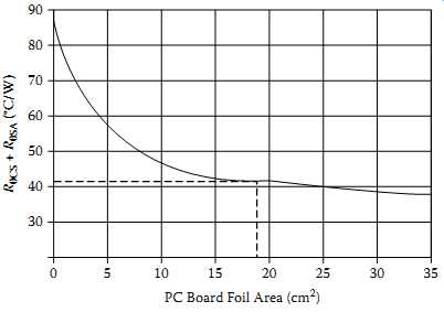
FIG. 18 Thermal resistance from case to ambient with PC-board foil area.
FIG. 19 Crowbar protection for overvoltage conditions: (a) implementation
of a simple crowbar circuit using limited components; (b) independent crowbar
units in an ORed redundant power supply system.
The designer should be able to calculate the maximum possible power dissipation for a given environment and then translate that value to safe maximum output currents based on approximate relationships for the given circuit and the topology. Another aspect is the transient thermal response, and in this situation an electrical equivalent of an RC element combination can be used with a simulator such as SPICE to generate the thermal response of a power semiconductor (60). Using a similar RC equivalent approach, when thermal simulation software is not available, or for quick calculations, designers can apply linear superposition to model the thermal performance of systems. Within the last decade, many new cooling systems have been introduced, and designers should consider these systems, such as microchanneled heat sinks (63) and nonlinear fin pattern-based systems (64), in very high power designs.
2. Overvoltage and Overcurrent Protection
2.1 Overvoltage Protection
A power supply should not generate any steady or transient overvoltages under all operating conditions, particularly in low-voltage, high-current power supplies. Sometimes an unexpected component failure, such as a shorted power transistor in a buck converter, can generate a disastrous high output voltage. Under a very peculiar and unwarranted load current transient, the power supply may generate a transient overvoltage condition.
In most situations, the easiest way to protect the load from overvoltage is to use crowbar circuits, which detect the overvoltage situation quickly and activate a short circuit across a fuse. To enable reliable protection, the overvoltage protection must be independent from the rest of the system's circuits; it must have its own voltage reference source and an independent power source. FIG. 19(a) indicates a simple implementation of a crowbar circuit (65) in a nonisolated synchronous buck converter. FIG. 19(b) indicates a case of diode-ORed redundant supplies with independent crowbar circuits.
In isolated power supplies, the transformer provides inherent protection against a switch failure; if any of the components in the feedback path opens accidentally, it can create a dangerous situation. Even in such situations, by using optoisolators, one can design crowbar protection circuits using parts similar to the case in FIG. 19(a) (65).
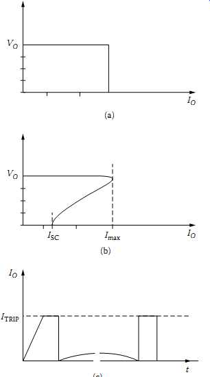
FIG. 20 Current-limiting methods: (a) constant current limiting; (b) foldback
limiting; (c) hiccup current limiting.
2.2 Overcurrent Protection
One of the most important protection features in the power supply is current limiting.
When designing a current limiter, one should think of two main aspects: measure the current and develop a limiting circuit using the current signal. Current limiter design necessitates trade-offs among cost, complexity, reliability, and performance. There are several possible current-limiting schemes, as shown in FIG. 20. In constant current limiting ( FIG. 20(a)), the output voltage drops sharply beyond the limit of the current.
In an LDO or a common linear regulator, if such a scheme is applied at the limit, the voltage across the pass element will exceed the normal operation value (from (Vin −
VO) to (Vin)) and the dissipation limit of the transistor and the heat sink can be exceeded, and the designer should allow for such excess dissipation. FIG. 20(b) shows foldback technique. An advantage in this scheme over the constant current-limiting method is that dissipation within the regulator circuits is minimized. The ratio of ISC/Imax is an important parameter for this scheme, where a smaller value means better performance.
However, unless the circuit is designed to reset automatically on removal of excess load, this scheme may need manual intervention at overcurrent. FIG. 20(c) shows the concept of hiccup current limiting. It incorporates overcurrent shutdown but adds an automatic restart mechanism. The power supply shuts down for a limited period of time and automatically restarts after a timeout.
In all these schemes, the traditional approach is to use a low-ohmic-value current sense resistor in series with the load path. To limit dissipation, a lower-value resistor needs to be used, or an alternative such as a PCB track as a resistance is logical. In all these situations, resistance value variation over the operational temperature range creates an uncertainty in the limiting value. When a copper PCB track is used, the approximate trace length can be determined using the following relationship:
...where I is the current value and R_sense is the expected resistance value in milliohms for a width of 20 mils/A (for 1 oz. type where the thickness is about 1.3 mils (33 μm) at 25°C).
FIG. 21 Current limiting in a synchronous buck regulator: (a) use of PCB
trace for sensing; (b) use of FET resistance for sensing.
FIG. 22 Transient protection for common- and differential-mode surges: multistage
surge suppressor with MOVs (M1 to M3), avalanche diodes (T1 to T3), and passive
parts.
In current-limiting schemes, the sensed current is used to activate the controller shutdown by an appropriate means of additional circuitry. In switching circuits with FETs, with the RDS(on) value for the FET available from the data sheets, one can develop a technique without a special-sense resistor, with knowledge of the converter topology (69). For the techniques used to activate constant current limiting or foldback current limiting in linear regulators, see Malley (70). FIG. 21 shows different concepts to achieve current limiting in a buck regulator (68). In shunt regulated DC power supplies, techniques can be developed for foldback without resistor based sensing (66, 71).
3. Protection against Input Transients
Due to acts of God, such as lightning or inductive load dumps on the AC input power supply, severe surge voltages may occur, and these transients are of very short duration, such as from 50 to 200 μs total. Almost all off-the-line power supplies need to be protected against such events where both common-mode and differential- (or transverse) mode transients can occur. In such situations, nonlinear devices such as metal oxide varistors and avalanche diodes can be combined with small inductors and capacitors, as per the representative schemes in FIG. 22. It’s important for the designers to subject these surge suppressor blocks, as well as the entire prototype of the power supply, to simulated surges, as specified under C62.41 or similar standards that specify surge-testing procedures and waveforms. More details are in Section 9.
4. Reliability of Input/Output Capacitors
One major family of components that can affect the long-term reliability of a switching power supply is the smoothing capacitors, which carry large ripple currents. In these components, such as the output filter capacitors or input filter capacitors, high-frequency ripple currents can flow at the switching frequency, and this can generate heat due to the ESR of the capacitor. Designers tend to select filter capacitors based on the capacitance value rather than the ripple current. This approach can be catastrophic, because ripple current ratings can vary widely among capacitor technologies, manufacturers, and voltage ratings. A typical example is the Nichicon PL series capacitors, with voltage ratings from 6.3 V to 63 V, where the RMS ripple current rating can vary from about 950 mA to about 2.4 A. Power dissipation inside a capacitor is mainly determined by its ESR and is approximately given by …
The ESR varies widely with the temperature and operating frequency; therefore the operating frequency of a switching supply and the temperature inside the case can have a significant effect on the amount of heat generated within the capacitor. The location of the capacitor within the power supply can also have a significant impact. For example, if output capacitors are placed closer to heat sinks or catch diodes, the heat generated in these external parts can also heat the capacitor. A capacitor's load life specification indicates how many hours the device is likely to operate under severe conditions, and the failure can be catastrophic or parametric. For aluminum electrolytic capacitors, the load life typically ranges between 1000 and 10,000 hr if operated around a maximum of 105°C. If such a capacitor is operated at a lower temperature, the load life is given by
... where L_actual is the actual lifetime and ΔTx is the temperature difference between the maximum allowable temperature and the actual temperature. The value of ΔTx is given by:
ΔTx = PCap/BA
…where B is the heat transfer coefficient (in W/cm^2/°C) and A is the surface area of the capacitor. B may not be available in the data sheet but can be obtained from the manufacturer. One problem arises in the calculation due to nonsinusoidal or DC-type current flowing inside the capacitor in the switching topology, and it varies with each topology. Huffman (72) provides these relationships based on idealized waveforms in each topology. To calculate the ESR at different temperatures, the ESR multiplier in FIG. 16 can be used. In multiphase buck converters, ripple currents can be improved significantly compared to single-phase versions (73).
Failures, Wearout, Time, Early life, Useful life, Low and constant intrinsic failure rate.
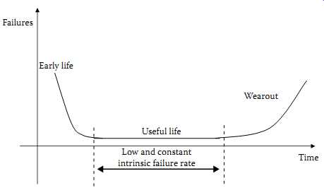
FIG. 23 Bath-tub curve as applied to product reliability.
10 Age-Related Aspects
The reliability of a power supply cannot be solely designed in, tested in, or built in. It takes a team effort, starting with the definition and specification of the product, and does not end with the first shipment to the customer. The following points are key to achieving a high-reliability power supply:
• A rigorous specification review-attention to all aspects of reliability, including packaging, cooling, and connectors
• Proven topologies with proven component sets
• A comprehensive qualification-emphasis on areas of concern such as power line disturbances, parametric variations, lifetime considerations, and extensive testing to specifications
• A rigorous life test, including on/off cycling
• Extensive box testing for electromagnetic compatibility, etc.
• Qualification of the vendor's production
• Analysis of field problems on a continuous basis to understand real failures
• Bathtub curve as applied to reliability of products.
A power supply is a typical product or subsystem that exhibits the typical bathtub curve, as in FIG. 23. The following tests are typical for achieving high levels of reliability:
• Thermal/shock cycling
• Temperature stress test
• Vibration
• EMI
• Thermal imaging (for an overall thermal profile)
• Stress analysis
• Power line disturbances
• Lifetime evaluation
• Test to specification
11 Testing of Power Supplies
The power supply is the heart of an electronic system, and it’s necessary for designers and test engineers to evaluate a supply's performance. This can be done at different stages, such as while refining the design or releasing the design. The most important basic tests are:
• Load regulation (graph of load current versus load voltage under fixed input voltage)
• Line regulation (graph of load current versus input line voltage under a fixed load current)
• Load transient recovery
• Current limiting
• Startup time
• Output noise (or periodic and random deviations (PARDs)) Other important tests are:
• Inrush current
• Line current
• Efficiency
• VID control (for VRMs)
During the design stage, it may be necessary to measure the loop performance for tuning the power supply's loop behavior.
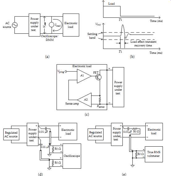
FIG. 24 Power supply measurements: (a) basic test setup; (b) transient parameters
for step load changes; (c) concept of an electronic load based on a MOSFET;
(d) noise (or PARD) measurement using oscilloscope; (e) noise measurement
using true RMS voltmeter.
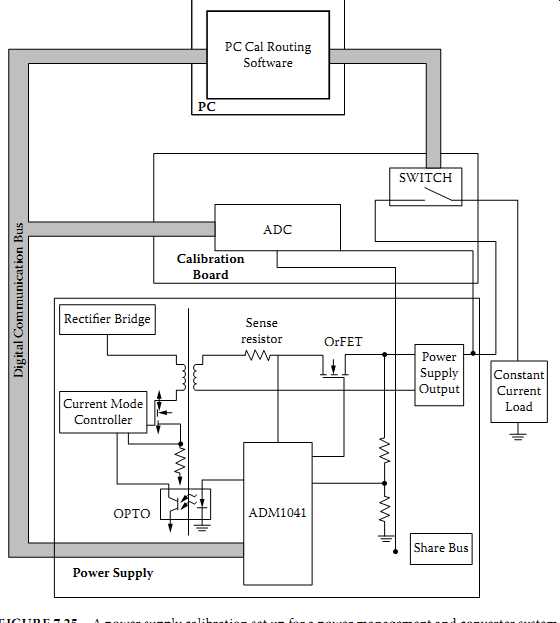
FIG. 25 A power supply calibration set up for a power management and converter
system designed around the ADM 1041 controller from Analog Devices, Inc.
Essential tests can be easily done using common bench instruments, such as a 5½-digit or better digital multimeter, a digital storage scope, and a reasonable electronic load.
FIG. 24(a) indicates a simple setup for load and line regulation. Load transient recovery, which is very important in high-current power supplies for digital processors, indicates one of the most important behaviors of the system, and FIG. 24(b) indicates the essential transient parameters to be measured using the scope. In this process, an electronic load, which allows us to program the current step (from high-to-low as well as low-to-high transition), is applied to the power supply being tested. Modern VRMs require very high slew rate capability, which can be in the range of 10-300 A/μs or even higher, and this kind of performance cannot be measured without a very high transient capability electronic load. FIG. 24(c) shows the concept of an electronic load based on a MOSFET and a current sense resistor. (In practice, the electronic load itself may be an expensive piece of equipment.) A few parameters of the electronic load are critical to reliable measurements:
• Response speed of the control loop in the electronic load (Tr)
• Total resistance of the shunt resistor and the RDS(on) of the MOSFET (R)
• Total connector inductance and the inductance of the MOSFET (L)
• Turn-on and turn-off time of the MOSFET (Tf)
• The maximum transient loading level of the step loading (I) Because the higher value of Tf or Tr determines the rise time of the electronic load (regardless of the load setting), this limits the transient capability of the electronic load.
For example, if this parameter is 1 μs, the maximum possible slew rates can be 10 A/μs and 100 A/μs for 10 A and 100 A loads, respectively. Details on these aspects can be found in Romanchik (76) and Lee (77). Such measurement may allow designers to tune the performance of a DC-DC converter (78). In POL converters used for processor circuit blocks, transient requirements can be in the range of 300 A/μs or more. Testing of these high-di/dt converters is discussed in Callanan (79).
Another important requirement is the measurement of noise or PARD, and this needs either a scope (for peak-to-peak measurement) or a true RF RMS voltmeter for RMS measurement. FIG. 24(d) shows test setups for PARD measurement. In this process, if the scope inputs are ground referenced, the use of differential probes is necessary.
As discussed in Section 5, feedback loop measurements require breaking and injecting a small AC signal, and this may not be easy because monolithic ICs used as controllers don’t allow opening up the loop. In such cases, alternative methods may be utilized. Another recent development is that of automatic routines and software that allows the calibration of power supply design parameters. With component tolerances affecting a given design, one needs trimming of various voltage dividers and feedback loop components at different stages. Using PC-based calibration software, a calibration board containing ADCs, and switches, a power supply design can be automatically trimmed to refine the performance. FIG. 25 shows such a setup for a power supply design based on a controller and a power management IC such as the ADM 1041 from Analog Devices, Inc.