AMAZON multi-meters discounts AMAZON oscilloscope discounts
...
1 Introduction
In the modern world of electronics, there are three different basic approaches available for DC-to-DC conversion. These are the linear approach, the switching approach, and the charge pump approach. In a practical system, one can mix these three techniques to provide a complex but elegant, overall solution with energy efficiency, effective silicon or PCB area, and noise and transient performance to suit different parts of an electronic system. Switch-mode DC-DC converters, which is a very mature approach to the DC power supply requirements of energy-efficient, compact, and por table systems, was developed mostly around a few fundamental transformer-less topologies such as buck (step-down), boost (step-up), and buck-boost (inverting type), and their transformer-isolated derivatives such as the forward-mode converter, flyback converter, etc. These mature techniques utilize controller chips from various power IC manufacturers, and they have proliferated in most consumer electronic families.
For much higher power density requirements and larger power requirements, switchmode topologies such as push-pull, half-bridge, and full-bridge versions are used.
Another recent development was the use of single-ended primary inductance converter (SEPIC) topology, which has become popular in battery-powered systems.
In this section we consider the fundamentals of simple and common topologies, design concepts, and approaches in switch-mode power supplies (SMPSs) with a few design examples of how fundamental design concepts and practices could be applied to develop the power conversion stages based on switch-mode topologies. Due to space constraints, for detailed theoretical aspects and deeper design considerations the detail-minded reader is expected to refer to the many useful references cited.
2 Why Switch Modes: An Overall Approach
A low-voltage power supply subsystem must fulfill four essential requirements: (a) isolation from the mains, (b) change of voltage level, (c) conversion to a s table and precise DC value, and (d) energy storage. Given these needs, if we use a basic approach in power supply components for volume or weight reduction, the following essentials can be considered; and in a practical SMPS, designers combine all the following simple concepts to have a lower volume, weight, and efficiency where a higher switching frequency is used for energy conversion.
2.1 Transformers and Inductors
Transformers and inductors are the bulkiest components in a power supply. For a transformer, RMS voltage across a winding is given by the relationship:
Vrms = 4.44Bmax ANf
...where Bmax is the maximum flux density in the core, A is the cross-sectional area of the core, N is the number of turns, and f is the operational frequency. Given this relationship, and for a given core material where Bmax is a property of the material, for a particular core area if we can operate the transformer at a higher frequency, we can have a reduced number of turns for a required voltage across a winding. Hence if we have a DC power supply, and use a transformer core with a higher maximum flux density (without saturation) to transfer energy to a secondary winding, one can use a higher frequency to have a lesser number of turns. However, for a magnetic core material hysteresis loss (Ph) and Eddie current losses (Pe) can increase with the frequency due to following relationships:
…
In an overall sense it indicates that if we can use better magnetic materials with a higher operational frequency, we can make the size of a transformer small. Also, if we are to use inductors as filtering elements at higher frequencies, their impedance given by
2πfL will be higher at a higher frequency.
2.2 Capacitors in Power Supplies
Capacitors are used for two basic purposes in a power supply. They are: (1) in the rectification and filtering stage; and (2) used as high-frequency filtering. When we use a […] capacitor in a full-wave or half-wave rectifier operating at a frequency f, peak-to-peak ripple voltage (Vr p-p) is given by
… where IL is the average DC load current. Given this relationship, if we can rectify and filter the AC input voltage at a higher frequency for the same peak-to-peak ripple voltage, the required capacitor is smaller. Also, in a general high-frequency filtering need where the high frequency needs to be bypassed to ground by a capacitor, we can use a smaller capacitor at a higher frequency, as the impedance of a capacitor is 1/2πfC. In summary, for filtering of ripple superimposed on a DC rail or for general filtering, the required capacitor size is smaller at a higher frequency.
2.3 Heat Sinks
In a linear power supply, a series pass element dissipates a higher wattage, due to the higher voltage across the pass element. However, if the transistor can be con figured to operate as a switch, dissipation will be lower and required heat sinks can be relatively small. In switch-mode power supplies, this concept is effectively used.
3 Basic Switch-Mode Power Supply Topologies
Commonly utilized switch-mode supplies could be subdivided into two basic kinds, non-transformer isolated and transformer isolated. Non-transformer-isolated versions are used in lower power requirements with no necessity to have electrical isolation from the primary energy source. Transformer-isolated topologies are used in higher power requirements, and they come with electrical isolation from the primary supply side. In the following sections we discuss the basic topologies and their fundamental operational relationships.
3.1 Non-transformer-Isolated Topologies
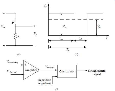
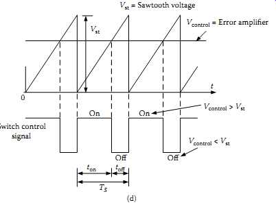
FIG. 1 Simple switching converter: (a) basic circuit without energy storage
components; (b) timing diagram; (c) block diagram of a pulse width modulator;
(d) comparator signals.
Several commonly used non-transformer-isolated topologies are: (a) buck or step-down converter; (b) boost or step-up converter; and (c) buck-boost or inverting type converter.
In all three topologies, four basic components (switch, inductor, capacitor, and a diode) are con figured in different ways to achieve DC-DC conversion while using a power semiconductor as a switch. Another very commonly used version is called the single-ended primary inductance converter (SEPIC), which is very much used in modern battery-powered portable systems. To provide an overview of the essential concepts used in these, FIG. 1(a) depicts a simple resistor in series with a switch that operates at a switching frequency of fc where the total cycle time Ts is comprised of an on time of ton and an off duration of t_off. FIG. 1(b) depicts the output voltage appearing across the resistor R and with an average value of Vo. FIG. 1(c) illustrates a basic concept to generate the switch control signal using a simple amplifier and a comparator.
FIG. 1(d) depicts the comparator signals. In the basic circuit of FIG. 1(c), a reference signal with a precisely controlled DC voltage is applied to the noninverting input of the amplifier, and the inverting input is supplied with the actual output. Comparator is supplied with a sawtooth waveform of peak voltage Vp and the control signal created by the output of the amplifier, vc, where the combination generates a pulse width modulated (PWM) signal as in the lower trace of the FIG. 1(c). In this situation, the duty ratio can be expressed as …
3.1.1 Buck Converter
FIG. 2(a) depicts the basic arrangement of a buck converter. A controller that has the fundamental characteristics similar to a case described in FIG. 1(c) can be used to toggle the power switch based on the level of the regulator output. In our analysis here we assume that the four basic components in the power stage, namely the switch, inductor, capacitor, and diode, are ideal. Under these ideal conditions, when the switch is on, if the output capacitor C is very large, the inductor will have a voltage difference of
(Vin-Vo) and this will cause the inductor current, iL, to rise steadily until the end of first phase of the switching cycle. FIG. 1(b) depicts the equivalent circuit when the switch is on. Under this condition, …
At the end of the on time, ton, the inductor current's only path to continue is through the diode, and if we consider the diode to be an ideal one, new voltage across the inductor will be -Vo and this will cause the inductor current to gradually decrease until the end of the off time of the switch, toff . See FIG. 2(c) for an equivalent circuit. Under this condition,
−V = L di dt o L
Under steady-state conditions, neither the inductor nor the capacitor should accumulate energy continuously. Therefore to maintain the volt second balance during the full cycle of time Ts, ….
Given the ideal components, which creates the situation of FIG. 1(b) and FIG. 1(c) respectively, we can simplify Eqn. (8) to, …
If D is the duty ratio, this can be reduced to...
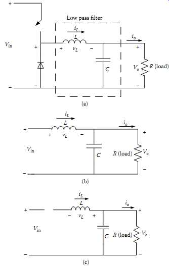
FIG. 2 Buck converter: (a) basic arrangement for DC-DC conversion; (b) first
state when the switch is on; (c) second state when the switch is off; (d)
waveforms.
It’s important to note that this condition is applicable only to the case where during the off state of the switch, inductor current does not reach zero, which is termed the continuous-conduction mode (CCM). FIG. 1(d) indicates the waveforms related to this case.
Under this condition, if all the components are ideal, input power should be equal to output, where …
From Eqn. (10) and (11), we can achieve the following relationship similar to the case of an ideal transformer:
Also, it’s important to observe that the instantaneous input current i_in keeps rising to the peak value of the inductor current, and suddenly drops to zero when switch is off.
This situation can create sharp voltage fluctuations at the input, and it’s necessary to use a filter capacitor at the input.
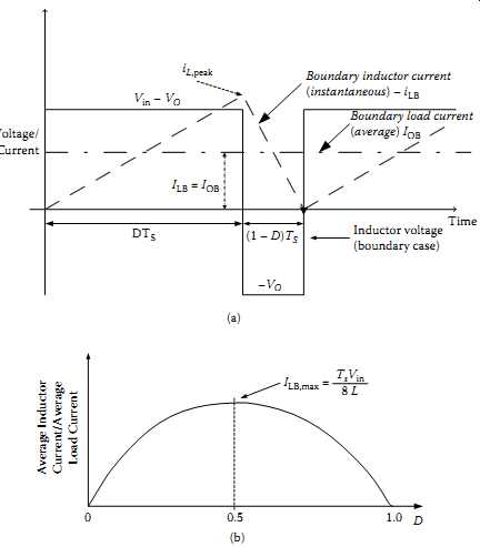
FIG. 3 Boundary condition between the CCM and the discontinuous-conduction
mode (DCM): (a) current waveform (b)ILB versus D when Vin is constant.
3.1.2 Buck Converter under Different Modes of Conduction
Given the conditions of the waveforms in FIG. 2(d), because the inductor average current IL should be the same as the average output current, if we keep reducing the load current, a condition will be reached where the inductor current will hit zero at the end of the switching cycle as shown in FIG. 3(a). If we keep reducing it further, there will be a period where the inductor current will be zero, during which period the capacitor will feed the load. Under this boundary case where inductor current reaches the zero value at the end of the switching cycle, inductor boundary current is given by…
FIG. 3(b) depicts the relationship between the duty ratio D and the boundary value of the output current IOB. As the graph in FIG. 3(b) indicates, the maximum value of the inductor boundary current occurs at D = 0.5. The practical implication of this relationship is that in a practical buck converter, for a given operating condition of Vd, Vo, D (which are the variable parameters) with selected values of the L and the switching frequency (1/Ts) in the design, when the load current, which is the same as the average inductor current, is below the value from Eqn. (13), the operation becomes discontinuous.
3.1.2.1 Analysis of the Case with Constant Vin
In a case such as in a motor speed controller, where input drive voltage is constant, Vo will be controlled by adjusting the duty ratio D; we can start our analysis referring to FIG. 1 (parts b and c). At the edge of continuous-conduction mode, also the relationship of Vo = DVin holds true. Therefore from Eqn. (13), …
This relationship leads to the graph of FIG. 3(b) and hence the peak value of boundary load current occurring at D = 0.5. At this maximum, we can achieve that…
In FIG. 4(a) the case of discontinuous mode is indicated where we maintain the switching frequency fs, L, D, and Vin constant while the load current keeps dropping below IOB. This makes the average inductor current drop below ILB and dictates a higher value for Vo than before, resulting in the discontinuous conduction mode (DCM).
In analyzing the case of DCM, from graphs in FIG. 4 we see that the inductor current is zero during the period Δ2Ts and the load current is now supplied by the output capacitor. Inductor voltage is zero during this period. Again considering the volt-second balance for the inductor during the switching cycle, …
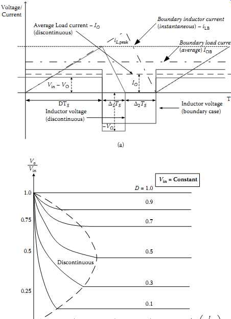
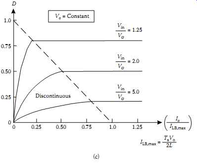
FIG. 4 Buck converter under discontinuous-conduction mode compared with
the case of boundary condition: (a) waveforms; (b) characteristics under constant
Vin; (c) characteristics under constant Vo. [...]
3.1.2.3 Output Voltage Ripple
One important output specification in a DC-DC converter is its peak-to-peak ripple, sometimes represented as a percentage of the average output DC voltage. In our previous analysis with ideal components, we assumed that the output capacitor C is very large, in order to assume that the output voltage will be constant. However, in a practical case where we have a finite capacitor value, we should be able to estimate the peak-to peak-ripple voltage, under high load currents, which usually creates the case of CCM.
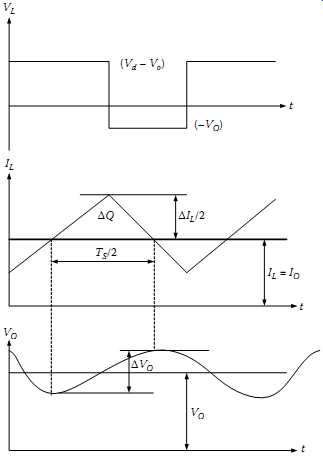
FIG. 5 depicts this case with the convenient assumption of an ideal capacitor
with zero equivalent series resistance (ESR).
Assuming that the average inductor current in the circuit is equal to the average load current, and the average ripple of the inductor current feeds the capacitor in each full cycle, for the CCM case, referring to FIG. 5, [...]
3.1.3 Boost Converter
Boost converter, or the step-up converter, as its name implies, converts the input voltage to a higher value, using the same four components in a power stage as per FIG. 6(a), controlled by a switching regulator converter IC. FIG. 6(b) indicates the waveforms under the CCM condition, and FIGS. 6(c) and 2.6(d) indicate the two different states.
Similar to the analysis in the case of buck converter under CCM, by considering the volt-second balance for the inductor for the whole period Ts, [...]
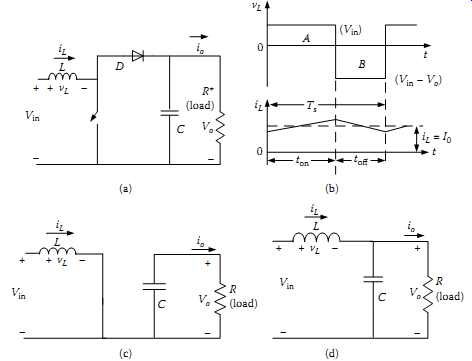
FIG. 6 Step-up converter: (a) basic power stage; (b) CCM waveforms; (c)
switch on state; (d) switch off state
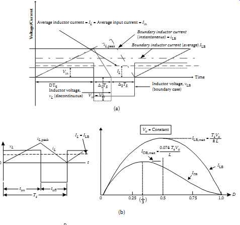
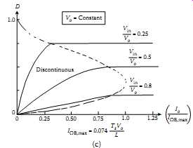
FIG. 7 Boost converter operation under different conditions: (a) waveforms
under boundary and DCM conditions; (b) graphs for operation under boundary
conditions; (c) graphs for DCM operation.
…available in [1]. In this case the average diode current will be equal to the average load current, and the instantaneous inductor current (iL) will be equal to the instantaneous input current (iin). FIG. 7(b) depicts the graphs for boundary condition for inductor current and the load current in relation to duty ratio D, when the output voltage is constant. FIG. 7(c) depicts the graphs for D versus output load current, for the ideal case, when the Vo is kept constant. Assuming a constant output current, the peak-to-peak ripple voltage can be expressed as a ratio of average output voltage given by ... FIG. 7(d) indicates the figures related to Equation (27), under CCM.
Though our ideal calculations for CCM give a simple ratio of ... for Vo/Vin, parasitic elements in the capacitor, inductor, switch, and diode will lead to a different situation as depicted in the graph of FIG. 8.
3.1.4 Buck-Boost Converter
By reconfiguring the same four elements as in the two previous topologies, we can arrive at another topology, buck-boost converter, which allows us to step up or step down the input DC voltage. FIG. 9 provides the CCM condition waveforms and two states of switching. An important observation here, as depicted in FIG. 9(a), is that the output DC voltage has a reverse polarity compared to the input. For this reason this is sometimes called the inverting configuration.
With a similar analysis to the two previous topologies, we can arrive at the following relationships for CCM:
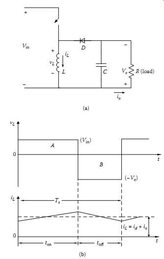
FIG. 9 Buck-boost topology: (a) power stage; (b) waveforms under CCM; (c)
state under on condition of the switch; (d) off state of the switch.
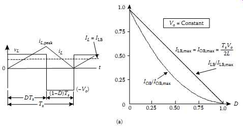
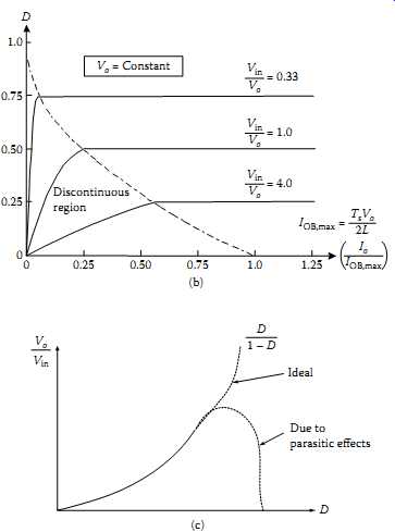
FIG. 10 Buck-boost converter performance: (a) boundary of CCM and DCM; (b)
general characteristics under CCM/DCM; (c) effect of parasitic elements in
power stage.
3.2 Transformer-Isolated Topologies
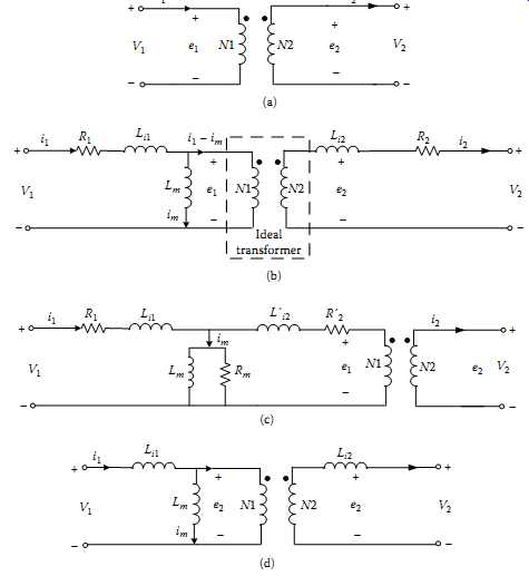
FIG. 11 Transformer equivalent circuits: (a) ideal case: (b) with components
indicating winding resistances, leakage inductances, and magnetizing inductance;
(c) inclusion of core losses and with further simplifications; (d) equivalent
circuit sui table for switching regulator calculations, neglecting all losses
in transformer.
Nonisolated basic converters (buck, boost, and buck-boost types) are generally used for lower-power PCB-level converter circuits and are not so popular for higher-power applications. Transformer-isolated versions such as forward mode, flyback, and bridge types are generally used for applications where higher power, galvanic isolation, and multiple-output rails are required. In the following paragraphs, a summarized overview on theoretical concepts behind these popular topologies is provided.
It’s necessary to use a transformer as a basic building block in these converters. In a quick revision on transformer theory, FIG. 11(a) indicates the case of an ideal transformer, and FIG. 11(b) indicates the case where practical conditions are taken into account, and in particular, (a) winding resistances, (b) leakage inductances of each winding due to flux not common to both windings (common flux in the core), and (c) a superficial winding (Lm) to represent the magnetizing requirement of the core. FIG. 11(c) indicates a case where core losses are also indicated. FIG. 10(d) indicates a simplified case where every secondary item is referred to the primary side, while assuming that the voltage drops across the windings (referred to primary) side are considered small, compared to the input voltage applied to the primary side.
Further discussion on this subject, as applicable to high-frequency switching transformers, is found below.
3.2.1 Forward-Mode Converters
The forward converter is derived from the buck topology family, generally employing a single switch. The power switch in the forward topology is ground referenced (also called a low-side switch), whereas in buck topology the switch source terminal floats on the switching node. The main advantage of the forward topology is that it provides isolation and the capability to provide step-up or step-down function.
FIG. 12 shows an idealized forward converter. Initially assuming that the transformer is ideal, when the switch is on, the diode D1 becomes forward biased, and D2 becomes reverse biased. Therefore ...
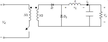
FIG. 12 Simplified forward converter without a demagnetizing winding.
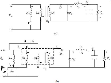
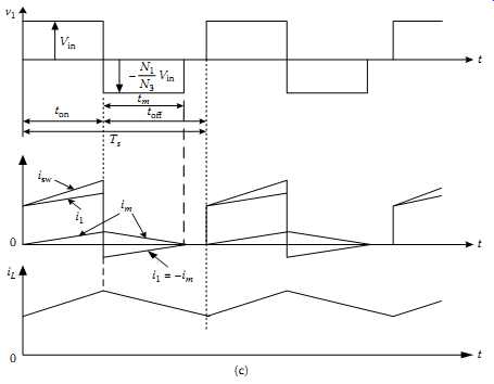
FIG. 13 Practical forward converter: (a) ideal case; (b) considering the
magnetizing inductance; (c) waveforms.
The above relationship indicates that the forward mode converter is similar to the buck converter behavior, however modified by the transformer turns ratio.
One important design consideration in this topology is the magnetizing inductance and the need to reset the transformer core. If the transformer core keeps building up any remaining core flux over each cycle, it will end up in saturation failure. FIG. 13(a) shows a simplified transformer-isolated forward converter with an additional demagnetizing winding and a diode connected in such a way that when the switch is on, the diode is blocked and vice versa. Therefore during the second part of the switching cycle where the switch is off, diode D1 gets forward biased and allows current flow in the third winding, to reset the core flux. When the switch is on,...
For the transformer to demagnetize before the next cycle begins, the maximum value for tm/Ts becomes (1 - D).....
In practice, it’s quite easy to construct a transformer where N1 and N2 are equal, and as N3 is used only to demagnetize the core, it does not require very much of an isolation requirement. This allows a bifilar winding to be used for N1 and N3. Under this case of N1 = N3, maximum duty cycle ratio, Dmax, becomes 0.5. Under this situation with a demagnetizing winding also it can be shown that,....
... which is the same case as per the ideal transformer with no demagnetizing winding.
Given the basic analysis of the idealized forward converter, it’s important to indicate that this is one of the very popular topologies in applications such as desktop computer power supplies like the "silver box," where the basic circuit can be modified to have multiple isolated windings, different core demagnetizing (resetting) techniques, or even multiple switches to share the current or the voltage stress across the drain and source terminals of the transistors. One important design consideration in this topology is the magnetizing inductance and the need to reset the transformer core. FIG. 11(d) shows a simplified transformer model including the magnetizing inductance (LM) and the leakage inductance (LL). The value of LM can be measured at the primary terminals with the secondary winding open-circuited (open-circuit test of a transformer). The peak current in LM is proportional to the maximum flux density within the core, and a given core can handle only a limited flux density before saturation occurs. At saturation, a rapid reduction of inductance occurs. The other element added to the transformer model is LL, and this can be measured at the primary terminals with the secondary winding(s) short-circuited (short-circuit test, usually conducted at a lower primary voltage such as 5%-10% of the primary rated value). This term represents the stray value, which does not couple primary to secondary. With careful design, this value can be kept small, and the effect on the converter is limited to voltage spikes on the power switch.
An important consideration in forward-mode converter design is the core-resetting requirement to avoid core saturation. A few techniques are available for this purpose in addition to the common method discussed in our basic analysis. A few advanced techniques used for solving the same problem are active clamp reset and resonant reset forward converters. FIG. 14 compares these techniques.
3.2.2 Flyback Converters
Flyback converters are derived from the buck-boost topology. Low cost and simplicity are the major advantages of the flyback topology. In multiple-output applications, the addition of a secondary winding, a diode, and an output capacitor is all that is required for an additional output. Flyback converter operation can lead to confusion if the designer approaches the design of its magnetics as if it were a transformer. Except for the case of multiple-output windings, the magnetics in a flyback converter are not a transformer. An easy way to view this is as an energy bucket that is alternately filled (when the switch is on) and dumped (when the switch is off). In other words, a flyback magnetic (sometimes called a transformer choke) is an energy-in, energy-out power transfer device where input and output windings don’t conduct current simultaneously.
A gapped core is used in general to have adequate leakage inductance at the input side for energy storage during the switch-on period.
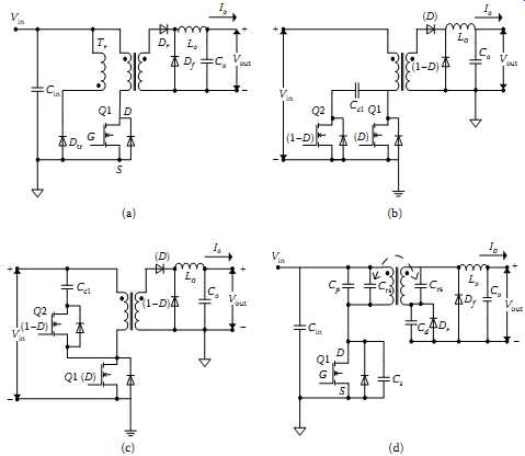
FIG. 14 Core reset techniques: (a) add-on winding and diode; (b) low-side
active switch; (c) high-side active clamp technique; (d) single-switch resonant
reset technique.
FIG. 15 depicts the simplified concept of this topology. FIG. 15(a) depicts the case of buck-boost topology rearranged to show the case of non-isolated flyback, and FIG. 15(b) depicts the transformer-isolated case. FIG. 15(c1) depicts the case where a two-winding inductor (which can act as a transformer or an inductor) is represented by its simplified equivalent circuit under on condition of the switch with the diode in reverse-biased condition, while FIG. 15(c2) depicts the case where the switch is off and the magnetic component is in transformer action, with the diode forward biased.
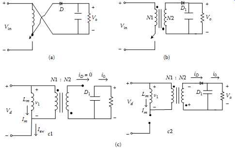
FIG. 15 Flyback converter: (a) rearranging the buck-boost as a flyback;
(b) transformer isolated case; (c) switch-on and switch-off modes; (d) waveforms.
This indicates that during the off period, the switch has to withstand a much higher voltage than the input maximum voltage. Given this situation, combined with the requirement to design the transformer to operate as an inductor-transformer, the process of design is bit more difficult than other topologies. Also, the transformer core design requirement becomes a bit more involved due to the need of an air gap in most cases, to have the right value for inductance Lm.
3.2.3 Push-Pull Converter
This is another popular converter topology with isolation, and FIG. 16 depicts the basic configuration of the power stage and the waveforms. In this case the center-tapped secondary winding is feeding the inductor alternatively. In the overall switching process, the switches on the primary T1 and T2 are alternatively switched with a dead time of Δ in the middle to avoid simultaneous switching of the two switches. When T1 is switched on, D1 conducts and D2 gets reverse biased. This causes a voltage difference across the filter inductor given by [...]
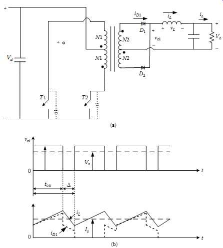
FIG. 16 Push-pull converter: (a) simplified power stage; (b) waveforms.
Antiparallel diodes on the primary side of the circuit allow a path for the current due to leakage flux of the transformer windings.
3.2.4 Half-Bridge and Full-Bridge Converters
Two other commonly used topologies are the half-bridge and full-bridge converters.
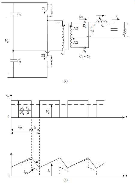
FIG. 17 depicts the half-bridge converter and its waveforms.
FIG. 18 depicts the full-bridge converter. In the half-bridge converter, the two capacitors C1 and C2 establish a midpoint voltage of 1/2Vin, and the two switches are alternatively switching on and off, similar to the case of the push-pull converter. By using similar principles of analysis, for the half-bridge converter we can prove that
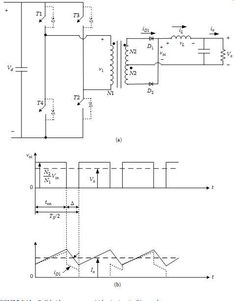
FIG. 18 Full-bridge converter: (a) basic circuit; (b) waveforms.
4 Applications and Industry-Favorite Configurations
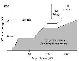
FIG. 19 Industry-favorite configurations.
Some relative merits and demerits of the switching converter topologies and typical applications are summarized in subsets of Section B, including essential mathematical expressions for important design relationships. The industry has settled on several primary topologies for a majority of applications. FIG. 19 illustrates the approximate range of usage for these topologies. The boundaries to these areas are determined primarily by the amount of stress the power switches must endure and still provide reliable performance. The boundaries delineated in FIG. 19 represent approximately 20 A of peak current in power switches.
Nonisolated basic converters (buck, boost, and buck-boost types) are generally used for lower-power PCB-level converter circuits and are not so popular for higher-power applications. Isolated versions such as forward mode, flyback, and bridge types are generally used for applications where higher power, galvanic isolation, and multiple-output rails are required.
As shown in FIG. 19, bridge converters are generally used for higher-power and higher-voltage converters because there are several power switches to share the dissipation and the voltage stress. In general, full-bridge topology is used for very high power applications, and it’s quite important to consider the losses in the circuits and the design complications due to their high-side switches operating with their source terminals (in the case of MOSFETs) or emitters (in IGBTs or power transistors) at floating levels. As indicated in the topology diagrams in Appendices B9 and B10, the transistors on the upper parts of the bridge (high-side transistors) require special circuitry to drive floating gate terminals.
Gate driver ICs help solve this problem. In a high-power DC-DC converter design, to achieve adequate efficiency the designer should develop an "efficiency budget" or a loss calculation. In general, losses are contributed by many different sources, the important ones being:
• Rectification losses (low-frequency rectifiers on the input side and high-frequency rectification circuits on the output side)
• Switching losses in power semis (static and dynamic dissipation)
• Core losses in magnetic components
• Losses due to control and supervisory circuits
• PCB losses associated with high-current tracks of the PCB
Using a simple calculation based on an Excel spreadsheet, the designer can determine where optimization can be achieved. FIG. 20 indicates the losses associated with a switching power supply with an output capacity of about 10 W. In a larger-capacity power supply, the percentage values may be different.
4.1 Use of Gate Driver ICs in High-Power Converters
The essential idea of a gate driver IC is to achieve two important design requirements: to provide correct voltage drive levels required by the MOSFET or IGBT gates where floating voltages are required, and to provide fast charge/discharge gate capacitances for MOSFETs or IGBTs. For example, in half- or full-bridge circuits based on MOSFETs, low-side (n channel) transistors need to be driven by a positive gate voltage with respect to the ground plane, but the high-side transistor gate needs to be driven by a positive voltage with respect to its source terminals, which will be at floating voltage values. TBL 1 shows the different techniques used for gate driver circuits and their key features [7]. Gate driver circuits are useful in any switching system topology where two switches operate at high and low sides. To justify the use of these for efficient power circuit designs, the designer should understand and pay adequate attention to the parasitic capacitances at the gate input [8]. For IGBT-based bridge topologies, there are hybrid ICs available as gate drivers [9]. In some of these, optoisolators are used for electrical isolation between the drive side and the power stage.
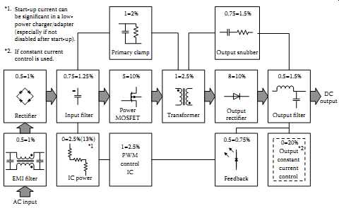
FIG. 20 Losses associated with a switching supply.
===
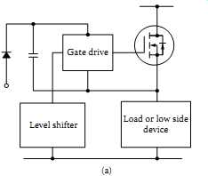
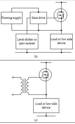
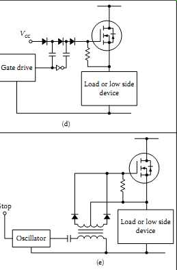
TBL 1 Comparison of Gate Driver Techniques
Comparison of Gate Driver Techniques
Technique Basic Circuit Configuration Features
Pulse transformer Load or low side device Gate drive Level shifter (a) Simple and cost effective
•Size increases with lower frequencies
•Operation over wide duty cycles need complex techniques
•At higher switching frequencies, parasitics come into play
•Bootstrap technique Floating supply Gate drive Load or low side device Level shifter or opto-isolater (b) Simple and inexpensive
•Duty cycle and on time are constrained by the need to charge the bootstrap capacitor
•At higher voltages, charging bootstrap capacitor may make up significant losses
•A level shifter is required
•Floating gate drive supply (c) Load or low side device Full gate control over wide range
• Level shifting can demand complex circuitry
• Cost due to isolated power supply for each high-side switch
• Optoisolator use can be relatively expensive
Technique Basic Circuit Configuration Features
Charge pump based
Carrier drive
Level shifting problems need to be tackled
Useful to generate a gate drive voltage above the rail voltage
Turn-on times can be too long Inefficiencies of voltage multipliers can require more than two stage capacitor circuits
Provides full gate control
Limited in switching performance
Could be improved by adding complex circuits
===
4.2 Single-Ended Primary Inductance Converter (SEPIC)
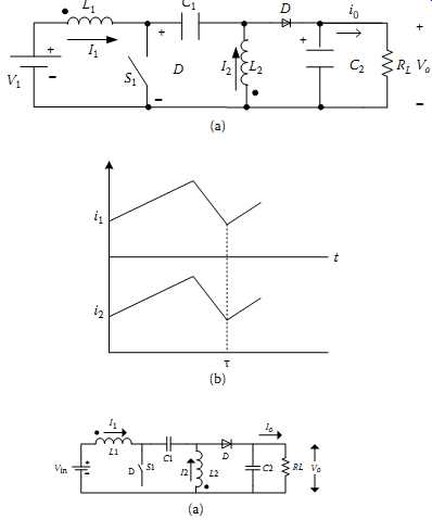
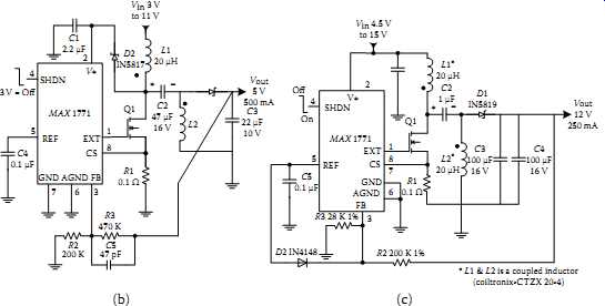
FIG. 21 SEPIC converter topology and application circuits: (a) basic topology;
(b) waveforms for the case when both inductor current are positive and continuous;
(c) a circuit for 5 V output from a 3-11 V input; (d) circuit for a 12 V output
from a 4.5-15 V input. (Because of the advantages of operation in buck or
boost modes without any voltage inversion, another popular converter used
in battery-powered applications is the SEPIC converter. Theoretical concepts
related to the SEPIC topology have been of interest since its development
in the mid-1970s. However, practical use of the technique was limited until
battery-powered applications proliferated, particularly Li-ion types, where
the battery pack's useful voltage can range from about 4.2 V to about 2.7
V.
The SEPIC is definitely worth considering for a typical portable system, in which 3 V circuitry is powered by an Li-ion cell. Although SEPIC circuits require more components than buck or boost converters, they allow operation with fewer cells in the battery, where the cost of extra components is usually offset by the savings in the battery. An important use of the SEPIC is in power factor correction (PFC). SEPIC topologies possess the following advantages:
• They have a single switch.
• They have continuous input current (similar to boost).
• Any output voltage can be used (as in the buck-boost case).
• Ripple current can be steered away from the input, reducing the need for input noise filtering.
• They have inrush/overload current limiting capability.
• Switch location is a simple low-side case, hence easier gate drive circuits.
• The outer loop control scheme is similar to a boost converter's case.
Disadvantages of the SEPIC are:
• They have higher switch/diode peak voltages compared to boost topology.
• They have greater bulk capacitor size and cost if operated lower than boost.
Referring to FIG. 21, SEPIC topology can be considered as an extension of the boost topology. When the switch S1 is on, current I1 flows into common rail via the inductor L1. Similarly, at that time current I2 flows through L2 where the capacitor C1 acts as a voltage source. When S1 goes off, I1 flows through C1and D into C2 and RL(load resistor). I2 flows through D into C2. Both currents ramp down as the capacitors are charged, and the load current flows from C2 to the load. (This is only one of the possible six operation modes of the topology [13].) This is the case where both inductor currents are positive and continuous as in FIG. 21(b). When this situation occurs, and equating the volt-second balances for each inductor L1 and L2 respectively, we can get the following relationships:
From these equations we get the transfer function as [...]
This indicates a case similar to buck-boost converter, but without any voltage inversion.
More details are available in [13]. A SEPIC converter can have six operating modes. A more detailed analysis with design approach can be found in [11-15].
FIGS. 21(c) and 21(d) show two SEPIC application circuits. Achievable efficiencies are about 85% [14]. Another useful practical consideration for easy construction and lower cost in SEPIC circuits is to have the two (nearly equal) inductors coupled [13,15].
Some trends of SEPIC applications and advancements are indicated in [16-30].
5 A Few Design Examples and Guidelines
There are about 10 different common topologies used in industrial and consumer applications, as summarized in Appendices B1 to B10, which include the topologies discussed in previous sections, and derived versions of flyback and forward converters such as two-transistor flyback and forward-mode converters.
A single-transistor flyback converter is an almost uncontested choice for off-line converters delivering fewer than 150 W. They are inexpensive because the transformer (which really works as a coupled inductor) is part of the output filter, and generating multiple outputs merely requires the addition of another secondary winding along with diodes and output filter capacitors.
However, at power levels greater than 150 W, because of excessive peak currents in the switching transistor and excessive voltages across the switches, this topology reaches its limitations. In these situations the two-transistor forward converter approach is a solution.
Design aspects and calculation guidelines for the two-transistor forward converter are available.
The following sections provide a guideline for designing practical DC-DC converters, with some examples of flyback and full-bridge topologies.
5.1 Flyback Converter Design Guidelines
A good application example of a flyback converter is an off-the-AC-line power adaptor for a notebook computer or a PDA. Based on the following specifications, one can start developing a flyback converter:
• Nominal AC input voltage (VAC_nom)
• Minimum and maximum AC input voltage (VAC_min and VAC_max)
• Output voltage (Vout) (a typical value is about 16 V)
• Maximum output overshoot, full load to no load (ΔVo)
• Maximum output power ( Po)
• Target efficiency at full load (η)
• Holdup time at nominal AC input voltage and full load at output (Thold)
Designing such a power adapter can be a challenge due to recent energy-saving initiatives, such as the European commission Code of Conduct Standby Power requirements, etc. FIG. 21 indicates a suggested configuration, as per guidelines.
The above data give the designer the necessary maximum input power,
[...] To design for low-input line situation with cycle skip hold-up time (when a short duration AC voltage failure) requirements, a minimum DC bus regulation voltage target must be selected and DC bus filter capacitance C3 in FIG. 22 must be calculated.
Based on an approximate DC bus typical voltage of VDC_typ(pk) = 2 VAC_nom, nominal value for DC bus bulk capacitor C3 can be calculated as [...]
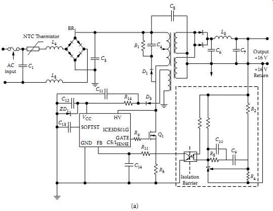
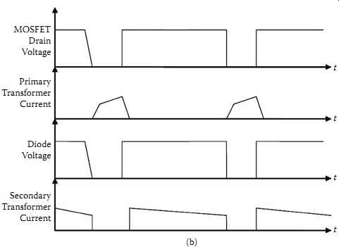
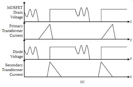
FIG. 22 A representative flyback converter and transformer current waveforms
related to different modes: (a) basic circuit arrangement; (b) CCM waveforms;
(c) DCM waveforms.
From this DC rail the circuit could operate in two different modes, namely continuous conduction mode (CCM) with a large primary inductance of the transformer-choke or in discontinuous-conduction mode (DCM) where primary current is shown in [...]
Assuming a maximum flux density value for the core (typically within 0.12 T to 0.3 T for a core such as an ETD30), a core can be selected from a magnetics manufacturer's data sheet. The core set and the gap must be chosen for an AL product that supports a reasonable number of turns in such a way that it meets the other requirements as well. The number of primary turns can be calculated as ...
... and rounded down to the nearest integer value. Then the secondary turns are calculated from the following:
…where V_diode is the estimated peak diode forward voltage and VR(max) is the reflected voltage on the primary. The reverse voltage for the rectifier diode, VR(Diode), is given by
... (In practice the value required may be much higher due to overvoltages related to parasitic inductances and the like.) For more details related to the DCM-type flyback converter, are suggested.
FIG. 22(a) indicates the essential circuit elements of a flyback converter based on a modern SMPS controller chip such as ICE3DSO1 from Infineon Technologies [33] with a power MOSFET driving the primary-side winding. Complete design details for an 80 W, 16 V power supply are given in [33].
5.1.1 Flyback Converters Using Power-Integrated Circuits
Another recent approach for flyback converters based on a complete power IC (an SMPS controller and a power MOSFET) is shown in FIG. 23 from Power Integrations.
FIGS. 23(a) to 23(d) indicate different levels of feedback circuit arrangements, where output regulation performance can vary from average (lowest cost) to extra-high accuracy. For more details related to these design approaches, see Leman [36] and Power Integrations, Inc. [37].
In this design approach, current waveform parameter KP simplifies calculations for both continuous and discontinuous modes [36]. For critical mode control-based design approaches. Flyback topology design using a MATHCAD-based approach . In this kind of design, for the best performance in charging a battery, the constant voltage mode (CVM), constant power mode (CPM), and constant current mode (CIM) are combined. It’s also possible to use either an active clamp or RCD clamp approach for transformer demagnetizing, and critical mode conduction is used on the boundary of the CVM and CPM regions.
5.2 Full-Bridge Converter Design Example-240 V DC, 1 kW Output DC-DC Converter with Planar Magnetic and Gate-Driver ICs to Drive the Switches of the Full Bridge
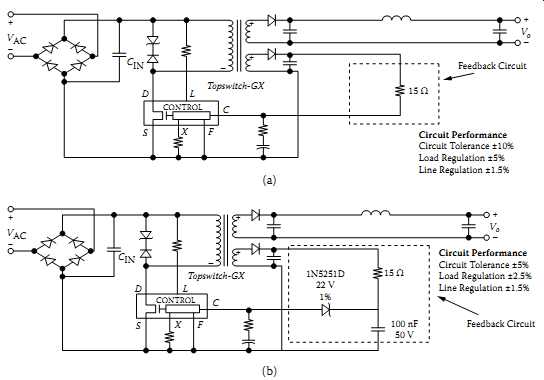
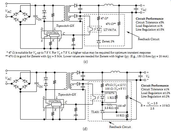
FIG. 23 Reduced component designs using power integrated circuits: (a) low-cost
version with simple feedback circuit; (b) with enhanced feedback; (c) opto/zener
feedback with tighter regulation; (d) opto/TL431-based feedback with excellent
load and line regulation performance.
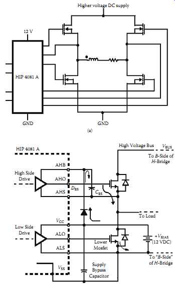
FIG. 24 HIP4081 MOS gate driver details: (a) basic concept; (b) bootstrap
capacitor arrangement.
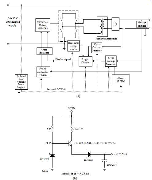
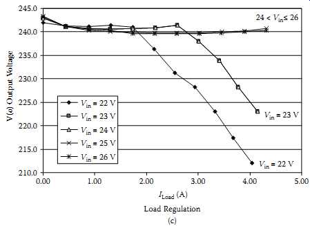
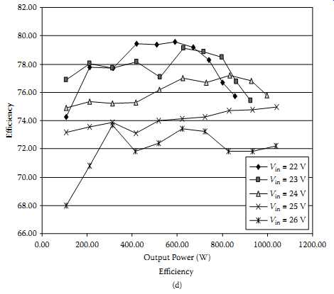
FIG. 25 Design approach to a 1 kW, 24 V input, 220 V DC output full bridge
with supervisory circuits and auxiliary power supplies: (a) overall design
approach; (b) kick-start power supply based on a simple circuit; (c) load
regulation; (d) efficiency.
Several years ago the author was asked to develop a DC-DC converter based on the following specifications:
• Input voltage: 20-30 V DC (nominal value of 24 V DC)
• Output voltage: 220 V DC at 1 kW output
• Topology: full bridge
• Switching frequency range: 150-250 kHz
• Transformer configuration: planar
• Regulation (load and line): ±2%
• Ripple: 0.5 Vpp
• Protection: overload, overvoltage, and over temperature, inhibit control
Several options were available for a project of this nature, and after considering hard switching PWM to resonant converters, the ultimate decision was for a Harris HIP 408Xbased full-bridge configuration, as shown in FIG. 24(a). In a design of this nature, the gate voltage required to switch on the upper transistors of the bridge should be floating above the source voltage, which will vary as the transistor pairs switch on alternatively.
HIP 4082 or a similar device is designed to achieve this requirement, and also provide a high charging current (in the order of 2.5 A max) to quickly charge the gate-source capacitance of the MOSFET. FIG. 24(a) provides the basic concept to achieve this condition. FIG. 24(b) provides the details of the MOS gate driver internals indicating the bootstrap capacitors, which provide the floating drive requirements to the upper MOSFETs.
With the requirement for an extremely compact version, with a percentage-efficiency target in the high 70s, an estimate of losses was done based on a set of MOSFETs with VDS = 70V, ID, max = 180A, and RDS(on) = 6mΩ (or better) as the four switches. The overall unit was expected to have an isolated low-voltage power supply for the control and supervisory circuits, as shown in the bottom left-hand corner of the FIG. 25(a). For initial startup requirements, a simple auxiliary power supply of 15 V was proposed based on a simple open-loop linear regulator. Once the 220 V DC output appeared, an auxiliary winding in the planar transformer would handle overpowering of the control and supervisory circuits. FIG. 25(b) shows this auxiliary (kick-start) supply. With the decision to hard-switch the PWM, a TL494 was chosen as the PWM controller. As indicated in the power stage of FIG. 25(a), a MOS_gate driver of the type HIP 4081 was used to simplify the design and to achieve a smaller PCB area after carefully considering the simplicity achievable by the pulse transformers. To achieve an extremely flat profile with a very small PCB area, a planar transformer from Payton America, Inc. was used. In achieving a low component count and associated high reliability, it was necessary to drop the temptation to use standard logic IC-based supervisory circuits and use (a component count optimized) simple comparator circuit-based subcircuit. A kick-start supply was used to power up the TL494 PWM controller, gate drivers, etc., during startup, and once the system started running, a single-turn auxiliary winding in the transformer would take over, increasing efficiency.
The efficiency achieved was about 75% at full load. The performance of the circuit is shown in FIGS. 25(c) and 25(d).