AMAZON multi-meters discounts AMAZON oscilloscope discounts
...
1 Introduction
All electronic circuits require a clean and constant voltage DC power supply. However, the energy source available for the system may be a commercial AC supply, a battery pack, or a combination of the two. In some special cases, this energy source may be another DC bus within the system or the universal serial bus (USB) port of a laptop. In a successful total system design exercise, the power supply should not be considered as an afterthought or the final stage of the design process, because it’s the most vital part of a system for reliable performance under worst-case circumstances. Another serious consideration in system design is the total weight and the volume, and this can be very much dependent on the power supply and the power management system. Also, it’s important for design engineers to keep in mind that the power supply design may entail many analog design concepts.
Most power supply design issues are due to resource and component limitations within the power supply and the power management system. Nonideal components-particularly, passives, commercial limitations to allocate sufficient backup energy storage within the battery pack, unexpected surges and transients from the commercial AC supply, and the fast load current transients-can create extreme and unexpected conditions within the system unless the power management system adequately addresses all the possible worst cases at an early design stage. Many product design experts choose to have the power supply and the power management system designed at an early stage with estimated parameters, with the actual system blocks powered from the system power supply.
This approach may help minimize late-stage disasters in a large design project.
In the 1960s and early 1970s, power supplies were linear designs with efficiencies in the range of 30%-50%. With the introduction of switching techniques in the 1980s, this rose to 60%-80%. In the mid-1980s, power densities were about 50 W/in3. With the introduction of resonant converter techniques in the 1990s, this was increased to 100 W/in^3 [1, 2]. When high-speed and power-hungry processors were introduced during the mid-1990s, much attention was focused on transient response, and industry trends were to mix linear and switching systems to obtain the best of both worlds. Low dropout (LDO) regulators were introduced to power noise-sensitive and fast transient loads in many portable products. In the late 1990s, power management and digital control concepts and many advanced approaches were introduced into the power supply and overall power management [3].
In this section we consider simple fundamentals related to an unregulated DC power supply and simple calculations to select the important components, with simple linear regulator concepts gradually extending to a discussion on LDOs. Because of space constraints, for detailed theoretical aspects and deeper design considerations, the reader is referred to the many useful references cited herein.
2 Simple Unregulated DC Power Supply and Estimating the Essential Component Values
In a DC power supply derived from the commercial AC source we can have two fundamental approaches: (a) transformer isolated and (b) nontransformer isolated.
Transformer-isolated power supplies are safer, but bulky due their line frequency transformer. This was the case for older electronic equipment where size was not a major concern, and still this approach is used in safety-critical applications or where common mode noise (discussed in Section 8) is a serious concern. Classic example in the modern scenario is the high-fidelity music systems. When the regulatory requirements for electrical isolation are covered by the DC-DC converters followed by the unregulated DC power supply, direct rectification and smoothing are used. One common example is the desktop computer power supplies (known as the "silver box"). In these incoming lines, voltage is directly rectified and filtered by a smoothing capacitor rated above the value of peak value of the AC line voltage, which is either 165 VDC (for 120 V, 60 Hz systems) or 325 VDC (for 230 V, 50 Hz). FIG. 1 indicates the concept.
Given the case in FIG. 1(c), if the peak voltage of the waveform of line frequency, f, appearing at the input of the bridge rectifier is Vpeak, the peak-to-peak ripple voltage at the output could be approximated by,…
Considering the capacitor is ideal, and the forward voltage drop for each of diodes is VD, the approximate output DC voltage, VDC, will be, …
These approximate relationships allow us to estimate the approximate design parameters for an unregulated DC power supply, with or without a transformer. In the case of an ideal transformer with a turns ratio of n, and the input AC line RMS voltage is Vrms, … Given the practical situations of path resistances, diode dynamic resistances, the equivalent series resistance (ESR) of the smoothing capacitor and the like, and any losses in the transformer, an unregulated DC power supply will have a load regulation curve as per FIG. 2.
3 Linear Regulators
Given the case of FIG. 2, an unregulated DC power supply needs further improvements to make the output DC voltage constant at different load current. Historically, with the availability of semiconductor components such as diodes and transistors, linear regulator techniques were developed to solve this load regulation issue. In the following sections, we discuss the linear regulator techniques in a brief manner to highlight the important considerations in linear regulator designs.
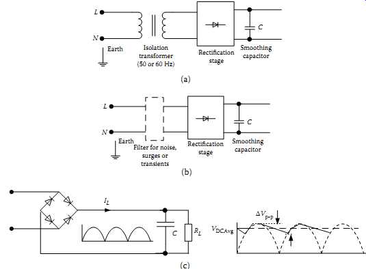
FIG. 1 Unregulated power supply derived from the commercial AC line: (a)
transformer isolated; (b) nontransformer isolated direct rectification; (c)
estimating the size of the smoothing capacitor.
===
Voc
For maximum RMS line voltage
For minimum RMS line voltage
VDC, min
I_max
Design margin
Voc(max)
Voc(min)
DC Output Voltage
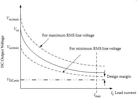
FIG. 2 Load regulation curve of a typical unregulated DC power supply.
===
In designing a regulated DC power supply, the designer should consider the output voltage changes due to three important situations: (1) output voltage variations due to load current changes (usually depicted in a load regulation curve), (2) output voltage variations due to input source voltage fluctuations (line regulation curve), and (3) output voltage variations due to temperature variations. To illustrate this let us take a very simple case of a shunt regulator based on a simple zener/avalanche-type diode. In designing a simple power converter of this kind, let us start from some specifications as below:
Unregulated input voltage range: 7 to 9 V DC Regulated output voltage: 5 V Maximum output current: 10 mA Output resistance of the unregulated input source: 10 Ω The most simple solution could be the circuit in FIG. 3 with a single resistor and a zener diode, where the regulated output is available at the terminals of the zener diode.
Given such a simple specification, if we are to develop this circuit from simple and basic calculations based on available commercial components, we can develop this circuit using a zener diode such as BZX84C5V1from ON Semiconductor. If we consider the overall circuit in FIG. 3(a), and the equivalent circuit for the diode in FIG. 3(b), we can design this circuit to achieve the approximate specifications given above. As the maximum load current expected is 10 mA, we can allow the diode to carry about 2 mA under full load situation. The diode we have chosen above has a nominal zener voltage of 5.1 at 5 mA, and the data sheet indicates a resistance of 60 Ω. With reference to FIG. 3(a), we can write the following relationships: [eqn. Not shown]
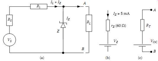
FIG. 3 Simple shunt regulator: (a) basic circuit; (b) simplified equivalent
circuit for a breakdown diode such as a zener or an avalanche diode; (c) simplified
representation of the power supply using Thevenin's equivalent circuit.
Based on the design conditions selected in the above paragraph, R1 can be estimated by applying the worst-case condition of lowest source voltage of 7 V and the case of zener diode taking up the whole current of 12 mA (when no load is connected), …giving a close enough E12 range resistor of 82 Ω.
When the input is at the maximum possible value and the circuit is on no-load condition, worst-case zener current occurs. This worst-case zener current is …
This gives a worst-case zener dissipation of (5.1 + 0.060*26)*26 =173mW, which is well within the data sheet limit. Under this condition the output voltage is approximately 5.1 + 0.060 * 26, which is approximately 6.7 V, and under worst-input voltage and maximum load current, output voltage is approximately 5.1 + 0.060 * 2), which is 5.22 V. This clearly shows that the output voltage can vary over a wide range, around an approximate value of nominal 5 V.
Given the variables in FIG. 3(a), using basic circuit theory we can estimate the approximate Thevenin's equivalent circuit parameters of the simple shunt regulator, as shown in FIG. 3(c). We can derive the Thevenin's equivalent circuit parameters as:
From these relationships, we can clearly see that the impact of input source voltage variations can be minimized by keeping the value of zener impedance, rz, much smaller than the value of (Rs + R1), and the same criteria applies to minimization of load regulation.
However, practical limitations of available diodes make these circuits useful only in very low current circuits. Also one major disadvantage of this kind of a circuit is the very high no-load power dissipation.
Based on the same simple example of the shunt regulator, we can develop a relationship for output voltage fluctuations in the form of,... where the coefficient k1 represents the Thevenin resistance, Ro, of the circuit, k2 represents the coefficient representing line regulation, and k3 represents the temperature coefficient of the power supply. If you take the simple example in FIG. 3(a) for a regulated power supply, when the load current is IL, output voltage Vo can be written as...
If the temperature effects on the breakdown voltage can be simplified by …
… where T is the absolute temperature, kT is the temperature coefficient of the zener, related to the nominal zener voltage, Vz,nom, at a specified temperature.....
The above discussion leads us to consider selection of devices with appropriate data sheet parameters to get the best possible specifications. For example, if we can select a diode with low rZ compared to the total input path resistance of (RS + R1), line regulation coefficient, k2, can be minimized.
While the above discussion leads us an example to developing suitable input-output relationships for the regulated power supply, if one requires better output regulation with higher output current capability, more advanced circuit configurations are required. FIG. 4 indicates two examples of more improved shunt regulator circuits.
In FIG. 4(a), R1 and Z1 act the same as in FIG. 3, where R2 and Z2 act as a preregulator.
In effect the preregulator provides a lower source resistance to the pair R1 and Z1. Relationships for this circuit can be developed using approximations applied to Equations (1.5) and (1.6). For example, if the preregulator can be developed with the useful relationships as applied to FIG. 3(a), the second stage sees very approximate Thevenin equivalent circuit with…
In effect this creates a condition where the regulator stage sees a near constant input and with a lower source resistance. If we can select the diode Z1 suitably, we get a more precisely regulated output. More discussion on this kind of circuits is in [1].
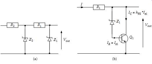
FIG. 4 Improved shunt regulator circuits: (a) a circuit with a better load
and line regulation;(b) a circuit with higher current capability.
When we need to achieve a higher output current capability, a transistor can be added to the basic circuit in FIG. 3(a), resulting in the case of FIG. 4(b). For this case, when the transistor is kept in the active mode,…
As the load sees the collector and emitter of the transistor, maximum load current is given by
This clearly indicates that it improves the capability by a factor nearly equal to the gain of the transistor.
3.1 Series Regulators
In all the above shunt regulator circuits, when the output current is zero the transistor/ zener dissipates lot of heat, and these circuits are generally used for low current requirements.
In general, series regulator concepts were more attractive to industrial applications and consumer electronics, except for their drawback of low efficiency. FIG. 5(a) depicts a very simple open-loop-type linear regulator. In general, the output regulated voltage V_Out can be approximated by,…
Under maximum load condition, if we need to maintain the zener diode voltage at the breakdown value, with a minimum current of IZ, min, current through resistor R1 under maximum load current will be ...
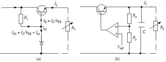
FIG. 5 The basic linear regulator configurations: (a) an open-loop type;
(b) a closed-loop type based on an op-amp in the control loop.
Given the above simplified analysis, we see that the regulated output has a severe dependency on the value of the VBE and the impact of the base current variations under load conditions. This leads to a case of coefficients in Equation (1.7) given by, … where IS is the saturation current and VZ is the nominal voltage of the Zener diode.
Given the above simplified analysis, we see that the regulated output has a severe dependency on the value of the load current also, in addition to the zener diode's temp performance.
Having discussed the basic behavior of an open-loop series regulator, we can use FIG. 5(b) to illustrate the basic elements of a closed-loop linear regulator, which can minimize some of these issues. Similar to the case in open-loop series regulator, the output is regulated by controlling the voltage drop across the series-pass element, a power transistor biased in the linear region. The control circuit compares the sample of the output voltage with a reference source, and changes the on-resistance of the series-pass power transistor.
If we consider the op-amp to be ideal, and the reference voltage to be constant at Vref, as far as the op-amp could maintain its basic function, Vout can be given by....
Given this simple relationship, we see that the circuit behaves much better than the previous cases of linear regulators, as far as the op-amp, and the reference sources are considered ideal. If a nonideal op amp with an open-loop gain of AOL and input resistance between the inverting and noninverting inputs is Rin, we can develop the following relationship for an output load current of IL as…
The power dissipation in the linear regulator is a function of the difference between the input and the output voltage, output load current, and power consumed by control circuits. The power dissipation in the series pass device contributes largely to lower the efficiency of linear regulators compared to switching regulators. Efficiency of a linear regulator can be approximated by ....
I_control is the current drawn by the control circuits, referred to the input side. This current is sometimes called the ground pin current (particularly in cases such as the three terminal regulators). This indicates to us that the best possible theoretical efficiency in a linear regulator is given by …
The major advantages of linear regulators in comparison with switching regulators are their (a) low noise, (b) transient response to load current fluctuations (output current slew rate), (c) design simplicity, and (d) low cost. However, due to the low efficiency of these circuits they are not attractive to high power requirements with wide differential voltage between the input and output sides. The following sections discuss the specifics of the essential components of a series linear regulator circuit.
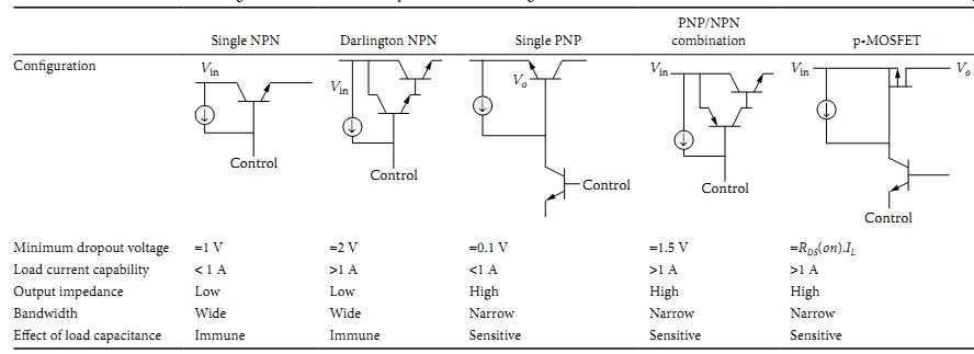
3.1.1 Series Pass Device
There are many different options for a series pass device of a linear regulator circuit, either in the form of a discrete design or in the monolithic IC form. TBL1.1 compares the characteristics of these options, as applicable to integrated circuits. In discrete form of circuits, the current capability could be much higher than the values in TBL1.1, but requires large heat sink to keep the series pass device within safe temperature limits.
Two possible circuit configurations are given in FIG. 6.
3.1.2 Control Circuits
The control circuit samples the output voltage through a resistive divider, and uses this feedback signal to control an error amplifier's output to control the resistance of the series pass device. Control circuit characteristics directly affect system bandwidth and the achievable DC regulation. The voltage reference is used for comparison of the output voltage in the control circuit, and primarily governs the steady-state accuracy of the device. The control circuit can be based on an op-amp or a circuit designed with discrete components. This directly governs the output transient response and the stability of the output. More on this will be discussed later. In general the designer should be conscious of the power consumption of the control circuits to get the best efficiency.
Any overcurrent or thermal protection needs to be incorporated into the control circuits, and FIG. 7 indicates a general block diagram.
3.1.3 The Output Capacitor
The bulk capacitance at the output maintains the output during transients. The output capacitor is required in order for the design to meet the specified transient requirements.
As with any control system, the voltage loop has a finite bandwidth and cannot instantaneously respond to a change in load conditions. The supply rail for many of today's microprocessors cannot vary more than ±100 mV while handling load transients of the order of 5 A with 20 ns rise and fall times. This translates to a current slew rate of 250 A/μs.
TBL 1 Pass Transistor Configurations and Their Comparison in Linear Regulators
In order to keep the output voltage within the specified tolerance, sufficient capacitance must be provided to source the increased load current throughout the initial portion of the transient period. During this time, charge is removed from the capacitor, and its voltage decreases until the control loop can catch the error and correct for the increased current demand. The amount of capacitance used must be sufficient to keep the voltage drop within specifications. Design considerations in the selection of the capacitor value are detailed in….
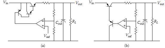
FIG. 6 Two possible linear regulator configurations: (a) with an NPN Darlington
pair for higher output current capability; (b) with a PNP series pass transistor.
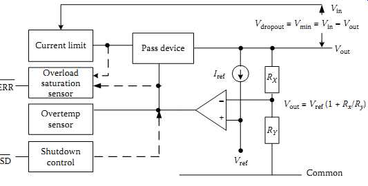
FIG. 7 Generalized block diagram of a linear regulator with additional protection
and external control inputs.
3.1.4 Voltage References
3.1.4.1 Voltage Reference Fundamentals
A wide variety of voltage references are available today. The most common ones are based on the action of either a zener diode or a bandgap cell with additional circuitry included to obtain good temperature stability. Although discrete zener diodes are available in voltage ratings as low as 1.8 V to as high as 200 V, with power-handling capabilities in excess of 100 W, their tolerance and temperature characteristics are unsuitable for many applications. Therefore discrete zener diode based references have additional circuitry to improve performance. One commonly used version is the temperature-compensated zener diode, particularly for voltages above 5 V.
The operation of a bandgap reference is based on specific characteristics of diodes operating at the same current but at different current densities. Bandgap references are available with output voltage ratings of about 1.2 V to 10 V. The principal advantage of these devices is their ability to provide low voltages such as 1.2, 2.5, or 5 V.
However, bandgap references of 5 V and higher tend to have more noise than equivalent zener-based references. This is due to the fact that in bandgap references, higher voltages are obtained by amplification of the 1.2 V bandgap voltage by an internal amplifier.
Their temperature stability is also below that of zener-based references.
In the commercial domain of semiconductors, there are several options today for voltage references such as (a) zener diodes, (b) buried zener diodes, (c) bandgap-based devices, and (d) XFET and FGA. A comprehensive account of these technologies is available.
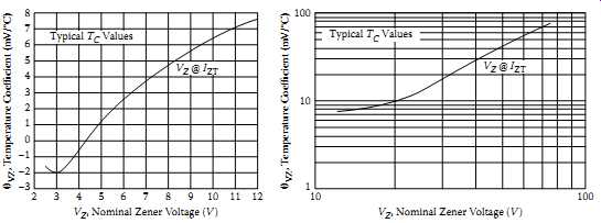
FIG. 8 Typical example of temperature characteristics of reverse-biased
silicon diodes: (a) Zener breakdown; (b) avalanche breakdown. (From Motorola-BZX
series.)
3.1.4.2 Reverse-Biased Diode-Based Voltage References
The most common and simple way to achieve a reference source is to use a reverse biased diode, or a zener diode as it’s commonly called, where it enters into a voltage breakdown region. A zener diode has two distinctly different breakdown mechanisms:
…zener breakdown and avalanche breakdown. The zener breakdown voltage decreases as the temperature increases creating a negative temperature coefficient (TC). The avalanche breakdown voltage increases with temperature (positive TC). This is illustrated in FIG. 8. The zener effect dominates usually below 5 V, and the avalanche effect dominates above 6 V. By the use of additional diode (in forward-biased mode) in series with an avalanche-type diode, it’s possible to achieve a better temperature stability in a reference circuit.
3.1.4.3 Bandgap References
This is one of the popular solutions to achieve a very stable reference source in a regulator circuit. The concept behind this circuit is to have two base emitter junctions operating at different current densities [4] where temperature compensation can be easily maintained. A circuit diagram of a bandgap reference is shown in FIG. 9. This circuit, developed by Paul Brokaw, is called Brokaw bandgap circuit. Transistors Q1 and Q2 are operating at the same current but at different current densities. This is achieved by fabricating Q2 with a larger emitter area than Q1. Therefore the base-emitter voltages of the two transistors are different.
This difference is dropped across R2. Extrapolated to absolute zero, VBE is equal to 1.205 V, the bandgap voltage of silicon, and has a predictable, negative temperature coefficient of -2 mV/°C. By adding a voltage to VBE that has a positive temperature coefficient, a bandgap reference can, at least theoretically, generate a constant voltage at any temperature.
The base-emitter voltage difference is given by ...
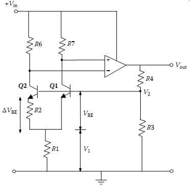
FIG. 9 The circuit diagram of a bandgap reference.
It’s shown that if ratio of the emitter areas of the two transistors is eight, the temperature coefficients of VBE and ΔVBE cancel each other. The op-amp raises the bandgap voltage V2 to a higher voltage at the output of the reference. There are many variations of this basic circuit in commercial bandgap references by Analog Devices Inc., USA, and readers can refer to their application notes for details.
Bandgap references typically provide voltages ranging from 1.2 V to 10 V. The advantage of bandgap references is their ability to provide voltages below 5 V. The greatest appeal of bandgap devices is the ability to function with operating currents from milliamps down to microamps. Commercial IC bandgap references have additional features such as multiple calibrated voltages. Because most bandgap references are constructed in monolithic form, they are relatively inexpensive. However, their temperature coefficient could be sometimes inferior to that of temperature-compensated zener-based references. This is due to second-order dependencies of ΔVBE on temperature.
3.1.4.4 Buried-Zener References
The above two types of common reference sources have their own advantages and disadvantages.
Another development to compete with disadvantages of these types was the buried-zener reference where some process improvements were used to get a lower noise and improved stability. Figures 10(a) and 10(b) depict some comparison of the device structure in relation to a regular zener diode. The device comes with a heating element to stabilize the temperature as shown in the commercial example of LM199 from National Semiconductor. Due to the difference in construction, it has achieved far superior performance, which can be summarized by,
• Very low initial error, between 0.01% and 0.05%
• Ultralow temperature coefficient, from 0.05 to 10 ppm/°C
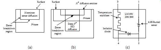
FIG. 10 Buried zener diode: (a) ordinary zener diode; (b) buried version
of the zener diode;
(c) schematic showing the heating element for temperature stabilization in LM199/299/399.
• Ultralow noise level of less than 10 μV peak to peak, in the frequency band of 0.1 to 10 Hz
• Long-term stability of typically less than 25 ppm/1000 hours More details can be found with historical developments occurring in Silicon Valley, USA. This will also provide more details on other state-of-the-art devices such as the XFET and Intersil/Xicor FGA types. Reference [5] provides some comparison of zener device families and bandgap families commonly available. Section A provides an overview of XFET.
3.1.4.5 Quality Measures of Voltage References
An ideal voltage reference would have the exact specified voltage, and it would not vary with time, temperature, input voltage or load conditions. However, as it’s not possible to fabricate such ideal references, manufacturers provide specifications informing the user of the device's important quality parameters.
3.1.4.5.1 Output Voltage Error
This is the initial untrimmed accuracy of the reference at 25°C at a specified input voltage. This is specified in millivolts or a percentage.
Some references provide pin connections for trimming their initial accuracy with an external potentiometer.
3.1.4.5.2 Temperature Coefficient
The temperature coefficient of a reference is its average change in output voltage as a function of temperature compared with its value at 25°C. This is specified in ppm/°C or mV/°C.
3.1.4.5.3 Line Regulation
This is the change in output voltage for a specified change in input voltage. Usually specified in %/V or μV/V of input change, line regulation is a measure of the reference's ability to handle variations in supply voltage.
3.1.4.5.4 Load Regulation
This is the change in output voltage for a specified change in load current. Specified in μV/mA, %/mA, or ohms of DC output resistance, load regulation includes any self-heating effects due to changes in power dissipation with load current.
3.1.4.5.5 Long-Term Stability
This is the change in the output voltage of a reference as a function of time. Specified in ppm/1000 hrs at a specific temperature, long-term stability is difficult to quantify. As a result, manufacturers usually provide only typical specifications based on device data collected during the characterization process.
3.1.4.5.6 Noise
Although the above are the most important quality parameters of a voltage reference, noise is particularly of importance in certain applications such as A/D or D/A converters. In such applications, the noise from the reference should be less than 10% of the LSB value of the converter. Therefore the higher the resolution of the converter, the lower should be the noise generated from the reference. Noise depends on the operating current of the reference, and is generally specified over a particular bandwidth and for a particular current. The specified bandwidths are 0.1-10 Hz (low-frequency noise) and 10 Hz-10 kHz (high-frequency noise).
4 Low-Dropout Regulators
As we discussed in section 1.3.1, if we can develop a linear regulator with minimized current consumption in the control circuits, and maintain the difference between the input and output voltages at a very low value, the circuit will be very efficient and will have all the valuable specifications of a linear regulator. Using the approximation in Equation (1.26), if we consider a linear regulator circuit with 5 V input and 3.3 V output, the efficiency will be around 66%. If the input is 3.5 for the same output, the theoretical best efficiency can be close to 94%, which is very much better than the efficiency of common switching regulators.
Based on the simple concept discussed above, to power modern por table devices such as cell phones, notebooks, and PDAs, a unique category of linear regulator ICs, low-dropout (LDO) regulators, have emerged during the last two decades. These were used in tandem with switching regulators to power noise-sensitive mixed-signal circuits, RF circuit blocks, and other noise-sensitive circuits. LDOs are available in a wide variety of output voltages and current capacities. Many LDOs are tailored to applications where a good response to a fast-step current transient is important. These devices have captured a large share of power management ICs in the early part of this decade [6]. This kind of a power supply solution is very helpful in low voltage rail based where load current can change rapidly, creating very high current slew rates [7].
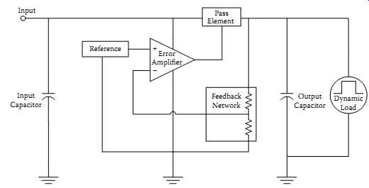
FIG. 11 Simplified block diagram of an LDO.
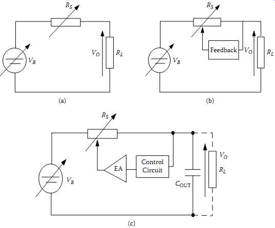
FIG. 12 Simplified concepts in LDO architecture: (a) two series resistors;
(b) circuit with feedback; (c) use of control circuit and an error amplifier
to implement the control loop.
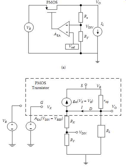
FIG. 13 PMOS LDO: (a) architecture; (b) small signal representation.
4.1 Basic Concept of an LDO
FIG. 11 depicts the simplified block diagram of an LDO regulator IC. The
main components are the pass element, precision reference, feedback network,
and error amplifier.
The input and output capacitors are the only key components of an LDO solution that are not contained within the monolithic LDO. TBL1.1 compares different options available for the pass transistor in a linear regulator and the advantages and disadvantages of the approaches. This is more applicable to modern LDO ICs. In discussing the details and design approaches to LDO-type regulators, let's start from the simple concept of FIG. 12(a). If we consider the case of battery input into an LDO where the voltage fluctuates as the load current varies, or as the battery drains the series resistance increases, it can be shown that to keep the output voltage, Vo, constant,… where VB and RS are battery voltage and the resistance due to the LDO series pass element respectively, while RL represents the load resistance. We can represent the same relationship as…
… where VLDO is the voltage across the series pass element. As depicted in FIG. 12(b), if we have a feedback circuit, the feedback circuit is expected to keep controlling the value of RS when VLDO fluctuates. As shown in TBL1.1, we can use any configuration of transistors as the series element, and in most new commercial LDOs MOS field effect transistors are used. FIG. 12(c) indicates the feedback loop arrangement with an error amplifier, which could be easily implemented by using an op-amp.
The basic PMOS LDO topology shown in FIG. 13(a) comprises an error amplifier that has the output voltage of VX and gain of AEA. The power transistor can be represented using the small signal equivalent model of transconductance gm and output resistance r_op as shown in FIG. 13(b).
According to the above representation in FIG. 13(b), current I can be written as ...
4.2 Important Parameters of LDOs
4.2.1 Dropout Voltage
This is the minimum voltage difference allowed for the series pass element before the regulator goes out of regulation. Usually a PMOS transistor-based version allows very low value and hence a high efficiency.
4.2.2 Input Voltage Range
This is the range of input voltages where the LDO remains in regulation. Lower value depends on the dropout voltage, while the higher end depends on the process capability, the heat sinking requirements, etc.
4.2.3 Regulated Output Voltage Range
This is the range of output voltage when the LDO is in regulation under steady-state conditions.
However, when the output load current changes fast, transient over- or undervoltage conditions may occur, which will exceed these limits for short durations.
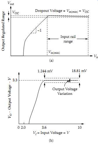
FIG. 14 Input output relationships of LDOs: (a) operation regions and parameters;
(b) performance of a typical commercial LDO from Texas Instruments.
FIG. 14(a) indicates the relationship between the input and output voltages, indicating the limits of regulation. FIG. 14(b) indicates the typical performance of an LDO such as TPS76333 from Texas Instruments, indicating the practical behavior of a 3.3 V output LDO.
There are many practically useful specifications defining the LDO characteristics.
These are summarized in TBL.2.
===========
TBL.2 Important Secondary Specifications of LDOs
Specification Description Remarks Output current range Output current handling capability of the LDO Minimum value depends on the stability of the output voltage at low current Maximum value depends on the safe-operating area (SOA) of the series pass device Load/line transient regulation A measure of speed of the LDO when the line voltage or load current fluctuates very fast Usually measured as a margin of allowed variation of the regulated output An important parameter in processor power supplies with high current slew rates Power supply rejection This is the ability of the LDO to reject AC ripple on the input side Short-circuit current limit Current drawn from the power supply when the output is short circuited Lower limit is determined by the maximum regulated output current Upper limit is determined by SOA of the pass transistor Output capacitor range Value of the output capacitance to operate within the stability range Most electrolytic capacitors have wide dependence on the temperature. Stability can be compromised due to this situation There are commercial LDO ICs that can also accept any capacitor value Overshoot At startup or during load current transients, output voltage may overshoot. This should be within a maximum limit
===========
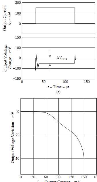
FIG. 15 Load regulation and transient performance of a typical LDO-TPS76350
from Texas Instruments: (a) load transient response; (b) steady-state performance
4.3 Application and Design Implications
A common application area of LDOs is the por table products where processors are coupled with many mixed-signal circuitries. In these circumstances two important specifications of a DC power supply become very dominant. These are the output noise and the transient response. Many processors frequently go through sleep and wakeup type sequences where the load currents vary suddenly from very low values to near maximum. These transitions in state-of-the-art products could generate current variations with current slew rates in the range of 10 A/μs to over 250 A/μs. Typical LDO load transient performance for a chip such as TPS763650 from Texas Instruments is shown in FIG. 15(a), while steady-state performance is shown in FIG. 15(b).
In FIG. 15(a), ΔVLDR indicates the steady-state response, which is the same value depicted in FIG. 15(b), but transient changes can always exceed this value as depicted in FIG. 15(a). In a well-designed LDO-based power supply, this transient fluctuation needs to be minimized.
In order to improve on the transient behavior, there are many improvements incorporated into LDO chips. One such example is the use of a fast transient loop in LDOs such as TPS75433 from Texas Instruments for low and high currents.
In the majority of LDOs and quasi-LDOs (where a composite NPN-PNP pair is used as the pass device), the pass device or the driver is a lateral PNP. Even though a PNP is better at providing a lower dropout voltage than an NPN [10], a lateral PNP is a low-frequency cutoff device with a poor transient response. For this reason, proper selection of the external output capacitor is important for the stability of the loop and adequate transient response. The compensation capacitor determines three key characteristics of an LDO: startup delay, load transient response, and loop stability. The startup time is approximately given by… where C is the value of the output capacitor and I_limit is the current limit of the regulator.
If C is fully discharged before the regulator is powered up, the regulator will limit current during startup, and the time to reach the nominal Vo will be delayed. Conversely, if C is too small, the output voltage will overshoot the nominal Vo during startup. Because it’s impossible to investigate all three characteristics at once, the designer should concentrate on first achieving a s table loop design and then check the startup delay and load transient response. In general if a single pole system can be created, and if the crossover frequency is selected to ensure that the system can quickly respond to load transients without undue ringing at the output, the design will be stable. For stability, the phase margin should be more than 45°. Unfortunately, an LDO has three dominant poles, and two are set by the regulator IC and the third is a function of the load and the output capacitor. The first pole, determined by the error amplifier, generally occurs between 10 and 300 Hz; the second pole, due to the pass device (or the PNP bias device of a compound regulator), is usually between 100 and 300 kHz. The third pole, set by the load and the output capacitor, occurs within the same range as the error amplifier or even slightly lower at light loads. FIG. 16(a) shows the simplified case of a load and output capacitor combination.
It can be shown that the pole and the zero created by the load are given by...
Based on the discussion in section 5, section 5.5, where added poles and zeros change the Bode plot, it’s apparent that the zero due to capacitor ESR modifies the total response of the circuit. FIG. 16(b1) shows the case where the output is marginally s table for ESR = 3.0 Ω. As depicted in Figure 3.16(b2), when the ESR is reduced to 1.0 Ω, the system's phase margin increases and the system becomes stable. When the ESR is lowered further, the system can become unstable, as in FIG. 16(b2). The capacitor used at the output should have some stability within the operational temperature ranges. Figure 5.16 shows typical aluminum electrolytic capacitor characteristics over frequency and temperature.
Based on the discussion related to FIG. 16, it’s important for designers to carefully examine the parameter changes of capacitors over frequency and temperature to achieve a stable design.
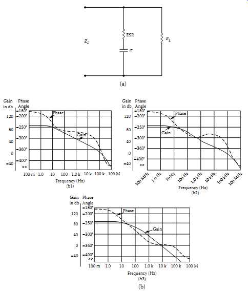
FIG. 16 Effect of the load on stability: (a) simplified load and output
capacitor combination; (b1) Bode plot of the output for a practical LDO based
on a regulator IC such as CS 8156 from ON Semiconductor for different cases
of ESR values: (b1) RO = 120 Ω and C = 22 μF with ESR = 3 Ω; (b2) RO = 120
Ω and C = 22 μF with ESR = 1 Ω; (b3) RO = 120 Ω and C = 22 μF with ESR = 0.01
Ω.
4.4 LDO Applications and Development Directions
LDOs have gained popularity with the growth of por table battery-powered devices.
Many circuit blocks in the portables such as cellular phones, cameras, and laptops have many noise-sensitive mixed-signal components, which may not tolerate the RFI/EMI issues of switching regulators. In these circumstances, LDOs or tandem combinations of LDO and switch-mode regulator are the only practical solution, provided that the efficiency issue can be managed. In most por table devices, LDOs are widely used as they occupy a very small PCB area and don’t use any bulky parts such as inductors and the like. LDOs are particularly attractive in systems with noise-sensitive system-on-chip (SoC) applications where battery power is used. LDOs also find applications in automotive environments because of the rapid voltage changes of the 12 V rail during cold startup [15]. Most LDOs are used in powering high-power processors where load current changes in step mode with high current slew rates. Schiff [16] and Rincon-Mora and Allen [17] provide design guidelines to deal with these conditions. With the initiatives to incorporate more commercial-off-the-shelf (COTS) components into military systems, some companies such as Linear Technology and others have developed high-reliability military plastic (MP) packaged LDOs with reverse voltage protection and current limiting over the full range of military operating temperatures [18]. Some devices such as LT3070 from Linear Technology could supply 5 A of load current at digitally programmable voltages from 0.8 V to 1.8 V with dropout voltages as low as 85 mV are examples of these MP-packaged devices. Details on frequency compensation of LDOs are available. For applications with extra low LDO voltages, ultra-low-dropout (ULDO) linear regulators based on bipolar CMOS-DMOS (BCD) technologies are available.
4.5 Low-Noise Application Requirements and Noise Measurements for LDO Output
Some of the LDO regulators are specially designed for low-noise requirements within cellular handsets and other por table applications, because most switch-mode power supplies are too noisy for these applications. The noise performance of these components sometimes needs to be quantified, and special measurement setups may be necessary.
In this process one should ensure that the LDO meets the system's noise requirement within the entire bandwidth of interest, typically in the range of 10 Hz to 100 kHz.
FIG. 17 indicates a sui table filter structure for testing the noise performance of LDOs in this frequency band. In LDO noise measurement, special consideration should be given to ground loop elimination; hence, all power supplies should be battery based, and thermally responding RMS meters should be used for measurements [23]. General performance verification of LDOs is discussed in Williams and Owen [24].
FIG. 17 Noise measurements for LDOs: (a) block diagram of a filter arrangement;
(b) a typical circuit configuration.
FIG. 18 Adjus table LDO circuits: (a) a simple circuit with two resistors to adjust the output;
(b) use of an adju stable reference source for improving accuracy.
4.6 Adjustable Output LDO Circuits
For applications where nonstandard voltages are required, an adju stable LDO is a good choice, but getting the highest accuracy from such an IC may require a few circuit tricks. FIG. 18 shows a few examples, including the use of an adju stable reference for improving accuracy [25]. For applications with hot-swap requirements, LDO ICs can be used with special current limiting arrangements.
4.7 Battery-Powered Applications and PMOS-Based LDOs
For battery-powered applications, PMOS-based LDOs provide accep table solutions. The factors to be considered include dropout voltage, ground current, noise, input voltage, and thermal response. Typical ground current components in an LDO are shown in FIG. 19(a). FIGS. 19(b) and 19(c) show the comparative performance of typical PNP LDOs and PMOS-based LDOs. For details, see Christ. Given the demand from many por table battery-powered applications, there is a considerable research effort on LDOs continuing at universities, and some of these are reflected in References.
References provide practical design guidelines for end users, including some thermal design aspects [34].
Another serious possibility is to have very high end-to-end efficiency-based supercapacitor enhancements to LDO-based linear regulator systems.
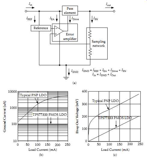
FIG. 19 Ground currents in an LDO and comparison of PNP and PMOS types:
(a) ground currents; (b) comparison of ground currents in PNP and PMOS types;
(c) comparison of dropout voltage in PNP and PMOS types.