AMAZON multi-meters discounts AMAZON oscilloscope discounts
...
1 Introduction
In our previous Sections on linear and switching regulators, our discussions did not consider the detailed aspects of the feedback loop used in the topology. In a well-designed DC-DC converter, irrespective of the load behavior, under all load currents the power supply should be free of any stray oscillations, and the DC rails should not fluctuate beyond specified margins. In a real-world, practical power supply design, when we consider the nonideal components such as op-amps, smoothing capacitors (with finite ESR), and inductors and transformers with parasitics, the design of the control loop becomes a challenge. This is further complicated by the finite frequency response properties of BJTs and MOSFETS, which have junction capacitances and other complex secondary elements. The subject of stability of a power supply that pertains to the closed-loop frequency response of the DC-DC converter has received much attention during the past quarter century. This Section provides a summary of essential theory and different practical approaches to get the best control loop design without a rigorous mathematical approach.
2 Feedback Control and Frequency Response
For most designers, feedback control loop stability is shrouded by a cloud of mystery.
Although most designers understand the problem of unwanted oscillations of a power supply, many use trial-and-error procedures or fancy mathematical models that require computing resources. In this section we discuss feedback loop stability, with some practical insights into the theory and suggesting some useful practical procedures for refining the design process.
A system that maintains a prescribed relationship between the output and the reference input by comparing them and using the difference as a means of control is called a feedback control system. Feedback control systems are often referred to as closed-loop control that uses the feedback control action in order to reduce the system error.
A typical block diagram of a closed-loop system is shown in FIG. 1. Closed-loop transfer function of this is given by...
... where R(s) is the input, output C(s) is obtained by multiplying the transfer function G(s), and H(s) is the feedback element form the output. More details can be found in Ogata (1).
Frequency response is the steady-state response of a system to a sinusoidal input. In frequency response analysis, frequency of the input signal is varied over a certain range and we study the resulting performance. In order to analyze control systems, frequency response analysis is a reliable approach that utilizes the data obtained from the measurements on the physical system without deriving the mathematical models. Frequency response methods are most powerful in the conventional control theory. An advantage of frequency response analysis is that this approach is simple in general and can be made accurately by ...
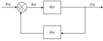
FIG. 1 Closed-loop system.
3 Poles, Zeros, and S-Domain
The frequency response can be analyzed by representing the gain as a function of the complex frequency s. The relationship between the input and output of a system, which is called the transfer function T(s), is derived as...
... Once this function is derived, by replacing s with jω we can evaluate its frequency behavior. In general, the transfer function T(s) in its own form (without substituting s = jω) can reveal many useful details about the stability of the circuit. The important thing here is to recognize that this function has a gain and phase associated with it. In such an equation the roots of the numerator N(s) = 0 are called zeros of the system, while the roots of the denominal D(s) = 0 are called the poles of the system. In general, function
T(s) can be expressed in many different forms, including:
... In Equation (5.3), Z1, Z2, … , Zm are called transfer function zeros or transmission zeros, and P1, P2,…, Pn are called transfer function poles or the natural modes of the network. The n of the transfer function is called the order of the network.
For example a first-order transfer function, which has a single pole, can be written as
... where P0 is called the pole frequency. (Sometimes first-order systems may involve one zero as well.) A second-order transfer function, which has two poles, can be written as
... where P0 and P1 are the pole frequencies. (Sometimes second-order systems may involve one or two zeros.) For example, a low-dropout regulator has three poles and one zero, which has a third-order transfer function, which will be discussed later in this Section.
4 Stability Using Bode Plots
Bode plots are convenient tools because they contain all the information necessary to determine if a closed-loop system is stable. Bode diagrams consists of two graphs, a logarithmic of the magnitude of sinusoidal transfer function and the phase plot, which is plotted against the frequency on logarithmic scale as shown in FIG. 2(b). In order to construct the Bode plot, first determine the transfer function and arrange the equation in the form of Equation (5.3).
A good place to start is the simple RC circuit, as in FIG. 2(a), and its gain and phase plot. For this simple single-pole circuit, the transfer function is given by
... and the pole frequency is given by....
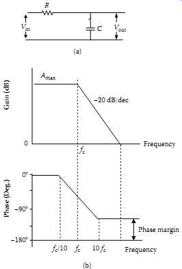
FIG. 2 Simple RC network and its gain and phase plots: (a) RC circuit; (b)
gain and phase plot.
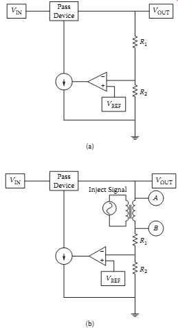
FIG. 3 (a) Simplified case of Figure 1.5(b) linear regulator; (b) modeling
technique to determine the loop gain of a linear regulator.
Equation (7) shows an important result, that a pole will cause the transition of the gain plot from 0 to −1 at a frequency of fc = 1/2πRC. At this corner frequency fc, the asymptote breaks and the slope is −6 dB/octave or −20 dB/decade. In general, a pole in a transfer function will cause a transition from +1 to a 0 slope, or 0 to −1, or −1 to −2, or −2 to −3, etc., with a gain change of −6 dB/octave (or −20 dB/decade). This is associated with a phase shift of −90°/octave or −45°/decade. Zeros are the points where the Bode plot breaks upward, causing an opposite change of slopes with leading phase shifts. More details in constructing Bode plots can be found searching Google.
5 Linear Regulators' Feedback and Loop Stability
As discussed in Section 1, all closed-loop-type linear regulator configurations use a feedback loop to hold the output voltage constant. In analyzing linear regulators, loop gain will be accounted as the magnitude of the voltage gain that the feedback signal experiences as it travels through the loop. In order to maintain corrected regulated output voltage and a stable loop response, it’s important to note that negative feedback must be used for a linear regulator. FIG. 3(a) illustrates the block diagram of typical linear regulator that applies this concept. The resistor divider, error amplifier, and pass element form a closed loop. The output voltage, VOUT, provides a feedback voltage through the resistor divider, to the inverting input of the error amplifier. The bandgap reference output (VREF) is a high-precision, fixed voltage that is tied to the noninverting input of the error amplifier. The error amplifier, essentially an op-amp, then makes fraction of output equal to VREF by sourcing a ground current to the base of the pass element. The pass element, in turn, supplies sufficient output current to keep VOUT at a certain value.
The regulated output voltage, therefore, is defined as ...
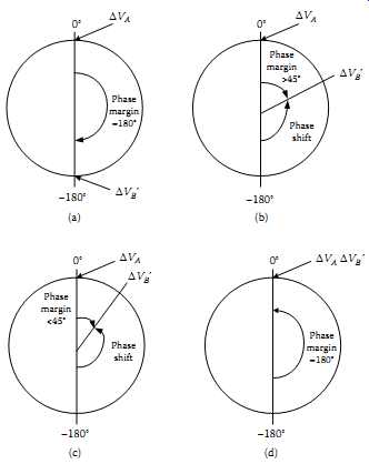
FIG. 4 Phase map: (a) perfect negative feedback-loop stable; (b) phase margin >45°-
loop stable; (c) phase margin <45°-loop unstable; (d) perfect positive
feedback-loop unstable.
This equation illustrates that the feedback is negative, and the adjustment of the output voltage resulting from the feedback is in opposite polarity to the "original" change to the output voltage. This means when there is a certain fluctuations in the output voltage by means of a rising or a falling of the output voltage (due to the changes in input voltage), the negative-feedback loop will respond to force it back to the nominal value.
In the analysis of feedback response in order to model the actual fluctuations on the output voltage, through a transformer a small sinusoidal signal is coupled to the feedback path. This small-signal sine wave is injected into the feedback path between points A and B and is used to modulate the feedback signal as shown in FIG. 3(b). The AC voltages at A and B are measured and used to calculate loop gain. Initially, the small signal has a value of ΔVA at point A, and a value of ΔVB at point B with respect to ground.
The signal at point B then travels through the loop and eventually arrives at point A, with a value of ΔVB'. Although ΔVA and ΔVB' have the same magnitude (unity gain), there is a difference in phase (in degrees) between the two.
If the error amplifier creates an ideal negative feedback to the loop, ΔVA would lag ΔVB' by -180° as shown in FIG. 4(a). However, because of the pass element's built-in capacitance, it introduces a phase shift that reduces the perfect -180° phase difference by a value between 0° and -180° (counterclockwise, with -180° as the starting point) as shown in Figures 5.4(b), 5.4(c), and 5.4(d). A stable loop typically needs at least 45° of phase margin. Phase margin (Ф) is a positive number (clockwise) between 0° and 180°, and is expressed as
Ф = 180° + phase shift
...where phase shift is a negative number that is counterclockwise between 0° and -180°.
To keep the loop stable, the phase margin must be no less than 45°. If a 45° phase margin cannot be achieved by the intrinsic architecture of the linear regulator, some form of compensation, either internal or external, is required.
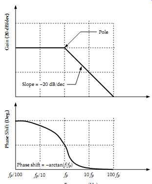
FIG. 5 Bode plot with pole gain/phase plot.
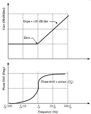
FIG.
6 Bode plot with zero gain/phase plot. Phase shift and phase margin can be
calculated easily using Bode plot analysis by means of poles and zeros. A
pole as shown in FIG. 5 is defined as a point where the slope of the gain
curve changes by −20 dB/decade with respect to the slope of the curve prior
to the pole. Each additional pole will contribute to increase the negative
slope by the factor N (−20 dB/decade), where N is the number of additional
poles. A pole also introduces a -90° phase shift (counterclockwise) from the
frequency one decade below ... pole frequency to the frequency one decade
above pole frequency, with a -45° phase shift at pole frequency.
A zero is defined as a point where the gain changes by +20 dB/decade with respect to the slope prior to the zero as shown in FIG. 6. Similar to the case of poles, the change in slope is additive with additional zeros. The phase shift introduced by a zero varies from 0 to +90°, with a +45° shift occurring at the frequency of the zero. The most important thing to observe about a zero is that it’s an antipole, which is to say its effects on gain and phase are exactly the opposite of a pole.
This is why zeros are intentionally added to the feedback loops of LDO regulators so that they can cancel out of the effect of one of the poles that would cause instability if left uncompensated.
5.1 Bode Plot Analysis
In order to analyze the effect of stability using poles and zeros in a Bode plot, let's consider an example of three poles and one zero as shown in FIG. 7.
It’s assumed that the DC gain is 80 dB, with the first pole occurring at 100 Hz. At that frequency, the slope of the gain curve changes to −20 dB/decade.
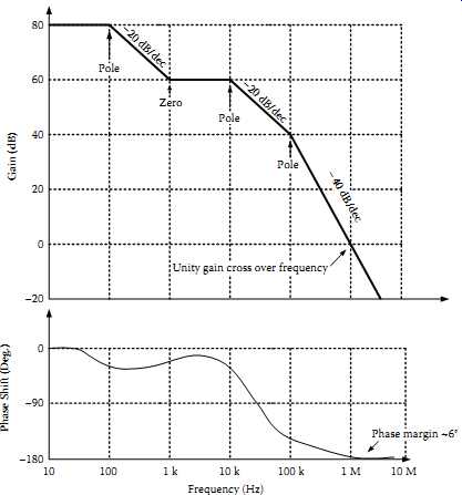
FIG. 7 Bode plot with phase information.
The zero at 1 kHz changes the slope of the gain to +20 dB/decade and the result of 0 dB/decade until the second pole at 10 kHz, where the gain curve slope returns to −20 dB/decade. The third and final pole at 100 kHz changes the gain slope to the final value of −40 dB/decade. It can also be seen that the unity gain (0 dB) crossover frequency is 1 MHz. The unity gain crossover frequency is sometimes referred to as the loop bandwidth where the gain of the loop reaches zero.
In order to get the phase plot, the phase shift at each frequency point was calculated based upon summing the contributions of every pole and zero at that frequency.
The first pole, next zero, and the second pole contribute their full phase shifts of −90°, +90, and -90° respectively, resulting in a net phase shift of −90°. The final pole is exactly one decade below the 0 dB frequency. Using Equation (5.10) for pole phase shift, this pole will contribute −84° of phase shift at 1 MHz. Added to the −90° from the two previous poles and the zero, the total phase shift is −174°, which results in a phase margin of 6°.
Therefore the loop is not stable and it would either oscillate or ring severely.
5.2 Stability Analysis
A linear regulator with an NPN pass transistor ( Figure 1.5(b)) is in the common collector configuration. For this configuration, considering the intrinsic factors of the pass transistor (at this stage we neglect the intrinsic factors of the error amplifier) the small signal equivalent circuit can be drawn as shown in FIG. 8.
The load current of the regulator can be written as ....
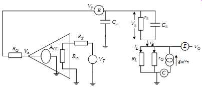
FIG. 8 Effects of intrinsic factors of an NPN pass transistor in the linear
regulator stability.
According to Equation (16) there is a pole that inherits from the intrinsic parameters of the pass transistor. Similarly, considering the error amplifier's intrinsic capacitances it can be shown that there is another pole due to the NPN linear regulator.
The following discussion shows the stability analysis for some practically available linear regulators configurations. The derivations are based on a similar approach to the above analysis.
6 Stability
6.1 Stability of Standard NPN Linear Regulator
The standard NPN regulator is based on the NPN Darlington pass transistor with PNP driver as shown in FIG. 9.
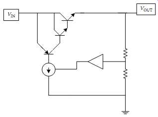
FIG. 9 Standard NPN regulator configuration.
As the pass transistor of the NPN regulator is connected in a circuit configuration known as the common collector, it inherits the low output impedance, which is an important characteristic of all common collector circuits. Therefore a power pole (PPWR), created by the pass element, occurs at a higher frequency because of the pass element's relatively low output impedance.
f(PPWR) = 1/2π.RPWR. CPWR
… where RPWR and CPWR are the pass element's resistance and capacitance.
The dominant pole (PINT), created by the intrinsic elements of the regulator, occurs at a very low frequency due to very high output impedance of the regulator especially due to the relatively high capacitance.
f(PINT) = 1/2π .RINT . CINT
… where RINT and CINT are the regulator's intrinsic resistance and capacitance.
According to the Bode plot analysis as shown in FIG. 10, there are two poles in the standard NPN regulator. Still, PPWR can occur at a frequency below the 0 dB crossover point, which may create a less than 45° phase margin. In this case, the loop becomes unstable, which creates a need for compensation (Graphs shown in dotted lines show the compensated case, with a phase margin greater than 45°. FIG. 10).
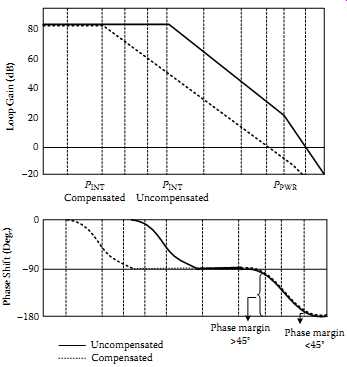
FIG. 10 Standard NPN regulator Bode plot (uncompensated and dominant pole
compensation).
In case of instability, the standard NPN regulator employs an internal compensation known as dominant pole compensation, which is achieved by adding intrinsic capacitance to the regulator so that PINT moves to an even lower frequency. Therefore the standard NPN regulator doesn't need an external compensation due to the superior frequency response of the NPN pass device.
6.2 Stability of Quasi-LDO Regulator
The quasi-LDO, as shown in FIG. 11, uses an NPN pass device, and it’s in the common-collector configuration, which means its output impedance is relatively low.
However, because the base of the NPN is being driven from a high-impedance PNP current source, the regulator output impedance of a quasi-LDO is not as low as the standard NPN regulator with an NPN Darlington pass device. Therefore PPWR occurs at a frequency lower than that of the standard NPN regulator, and usually below the 0 dB crossover point. The result is a less than 45° phase margin, where compensation is needed for loop stability ( FIG. 12).
Because of the relatively low frequency of PPWR, the NPN pass transistor regulator cannot be stabilized by using only dominant pole compensation. Instead, a zero must be placed between PINT and PPWR to increase the phase margin to at least 45° ( FIG. 12).
This is accomplished by using an external compensation method, such as the addition of an output capacitor next to VOUT. The frequency of the added zero (ZCOMP) is defined by
f(ZCOMP) = 1/(2π . ESR . COUT)
… where ESR is the equivalent series resistance of the output capacitor.
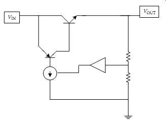
FIG. 11 Quasi-LDO configuration.
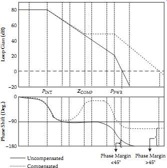
FIG. 12 Quasi-LDO regulator bode plot (uncompensated and dominant pole compensation)
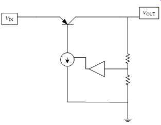
FIG. 13 Low dropout regulator configuration
Because PPWR of the NPN pass transistor regulator still occurs at a relatively higher frequency, output capacitor selection is fairly easy. As long as f(ZCOMP) is lower than f(PPWR), COUT can be small, and ESR is not critical.
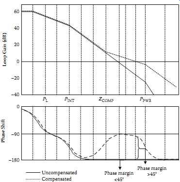
FIG. 14 LDO regulator Bode plot (uncompensated and dominant pole compensation).
6.3 Stability of LDO Regulator with a PNP Pass Transistor
Compared to other linear regulator configurations, PNP pass transistor regulator requires more careful selection of an output capacitor.
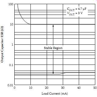
FIG. 15 ESR range of a typical LDO.
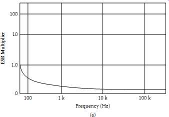
FIG. 16 Behavior of typical aluminum electrolytic capacitors at different
frequencies and temperatures: (a) frequency behavior; (b) ESR change with
temperature; (c) capacitance change with temperature.
Its pass element, the PNP transistor, is in a common emitter configuration, which exhibits high output impedance, so PPWR occurs at a frequency lower than in the other linear regulator configurations. Furthermore the impedance of the load, created by load resistance and output capacitance, becomes a significant contributor to loop stability by adding another low-frequency load pole (PL) to the Bode plot. The frequency of PL is expressed as
f(PL) = 1/(2π . RLOAD.COUT)
Typically, RLOAD and COUT are higher than the regulator's intrinsic resistance (RINT) and capacitance (CINT), which makes PL occur at a frequency lower than f(PINT). With three poles the PNP pass transistor regulator is not stable, even with dominant pole compensation. A zero must be added to compensate for this instability, which can be accomplished by the addition of an output capacitor next to VOUT. Particularly, the location of the zero in the frequency space is critical, because it translates to a careful matching of the output capacitor's capacitance and ESR.
The zero must occur somewhere between PINT and PPWR (FIG. 14). Because PPWR occurs at a relatively low frequency, the "space" between PINT and PPWR is narrow; hence, the choice of f(ZCOMP) is narrow and is demonstrated as:
f(PINT) < f(ZCOMP) < f(PPWR)/10
Equation shows that ZCOMP must occur above f(PINT), and at least one decade below f(PPWR). This is because ZCOMP needs the full one decade above f(ZCOMP) to fully realize its +90° phase shift. Based on Equation (5.21) in order to maintain loop stability at any given capacitance value, the ESR must satisfy the following:
RINTCINT/COUT > ESR > 10RPWRCPWR/COUT
If the ESR is either too high or too low, it’s out of range. The ESR is too high when the following condition exists:
ESR > RINTCINT/COUT
In this condition, ZCOMP occurs at a frequency below f(PINT). Additionally, because of the narrow space between PL and PINT, ZCOMP can be within one decade of f(PINT). This prevents ZCOMP from realizing its full +90° phase shift. As a result, the phase margin may not rise above 45° and, hence, the loop is unstable.
On the other hand, ESR is too low when the following is true:
ESR < 10RPWRCPWR/COUT (5.24) Here, ZCOMP occurs within one decade below f(PPWR), which prevents it from realizing its full +90° phase shift. Therefore the phase margin won’t rise above 45°, and the loop, again, is unstable.
The LDO manufacturer provides a set of curves that define the boundaries of the stable region, plotted as a function of load current ( FIG. 15). Furthermore the capacitor used at the output should have some stability within the operational temperature ranges. FIG. 16 shows typical aluminum electrolytic capacitor characteristics over frequency and temperature.
There are novel modifications to the basic LDO architecture from Analog Devices' ADP330X series LDO regulator family in which careful selection of output capacitor is not necessary required for these models. These regulators are also known as the any CAP• family, so named for their relative insensitivity to the output capacitor in terms of both size and ESR.
Leung et al. have analyzed and shown that the conventional frequency compensation cannot effectively stabilize a low-voltage LDO with a two-stage error amplifier.
Further they emphasized that the conventional technique is parameter dependent and very sensitive to external effect so is limited to certain operation conditions and not the optimum. In order to stabilize low-voltage LDOs, they have developed a novel approach based on nested Miller compensation, called pole control frequency compensation (PCFC), which is a systematic approach and improves the stability of the low-voltage LDO under load current and temperature.
Conventional ESR frequency compensation is not an optimal method to maintain stability for a wide range of loading current as the pole at the output node changes significantly with different loading conditions. Kwok and Mok (9) have introduced a tracking zero to cancel the output pole so that the frequency response becomes independent of the load current.
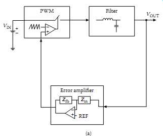
FIG. 17 Control loop as applicable to a switching power supply.
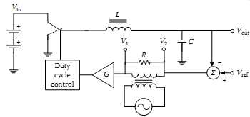
FIG. 18 Estimation of the control loop gain of SMPS.
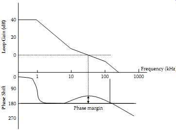
FIG. 19 Bode plot of a SMPS.
7 Feedback Loop and Stability of Switch-Mode Power Supplies
Any switching regulator also may be treated as a closed-loop feedback control system.
In analyzing the feedback loop and stability, the same Bode plot-based analyzing procedure of linear regulators is applicable to switching regulators as well.
Automatic regulation of the output voltage against fluctuations can be achieved with negative feedback. The difference between output voltage and a reference is sampled and used to control the duty cycle. Negative feedback reduces the duty cycle to lower the output voltage and vice versa.
For a closed loop of a switching supply, as shown in FIG. 17, the loop consists of two typical blocks: the modulator and the error or feedback amplifier. (The case shown is a simple buck converter only, but a similar simplified block diagram can be developed for any other configuration.) The speed and accuracy of voltage regulation depends on the total voltage "gain" around the complete switch, filter, feedback amplifier, and the duty cycle of the control loop as a function of frequency. The loop gain can be measured by injecting a small AC signal into the feedback loop using an isolation transformer as shown in FIG. 18 and measuring the ratio of the amplified AC error voltage (V2) to the injected signal voltage (V1) versus frequency.
To achieve overall system stability and adequate phase margin, the amplifier gain combined with the modulator gain should produce an overall gain plot that crosses the unity gain (0 dB) line at the desired crossover frequency as shown in FIG. 19 (similar to the case of linear regulators).
All off-the-line PWM switching power supplies consist of a modulator, an error amplifier, an isolation transformer, and an output LC filter. In single-port direct duty cycle control PWM power supply topologies, a voltage Vc is applied to the control port of the PWM comparator, and it’s compared to a saw tooth voltage of constant amplitude Vs to change the comparator's output duty cycle from 0 to 1. The resulting duty cycle of the drive waveform then varies as…
The gain of the buck family (forward, push-pull, and bridge) converters is given by p is the transformer secondary-to-primary turns ratio and Vin is the transformer primary voltage.
The control-to-output voltage DC gain of a PWM power supply is ...
Equation shows the gain H(s) of the system. For more details, refer to Chryssis (2).
An error amp based on the op-amp can be designed to have any pole-zero combination to change the Bode plot to attain unconditionally stable characteristics of the circuit.
The op-amp circuit can have different configurations, and in general there are three common types used in practical switching power supply environments. TBL. 1 shows the simplified circuit configurations and the associated transfer functions. In error amplifier configurations, such as in TBL. 1, break or corner frequencies are predetermined by the design objectives. Type 1 is a simple RC low-pass filter with a single pole; type 2 is with a pole-zero pair; and type 3 is with two pole-zero pairs. In type 3, loop crossover should occur between f2 and f3 for better stability. Another mathematical technique useful in this process is called the K-factor method, which is a mathematical tool for defining the shape and characteristics of the transfer function; more details can be found in Chryssis (2).
In practice, the overall loop can be complicated, and in the final stage of a design project, the design team can make use of some tests to measure the loop transfer function.
One test is to inject a signal into the loop and then measure the loop transfer function.
However, due to monolithic ICs that don’t allow injection of the signal in the best location, one may have to compromise with an "achievable method." FIG. 20 shows the case from Venable (21), where the desired versus achievable methods are indicated for a simplified case of a computer power supply. In FIG. 20, for the case of a common PWM control IC type UC 3844, two cases of feedback paths exist (a fast loop via resistor R5, and a slow loop via R7). Figures 20(a) to 20(f) show these measurements in this typical example (21). One practical difficulty with such measurements is to select an injection transformer with wide frequency response. Although some companies sell such transformers, they can be expensive. One solution proposed is to modify an off-the-shelf current transformer and use it with a typical network analyzer- based measurement setup. FIG. 21 shows a typical injection transformer setup with a network analyzer (22). Figures 21(b) and 21(c) show a typical frequency response curve for a commercial current transformer, such as the PE-51687 from Pulse Engineering (22). Williams (23) discusses practical guidelines for an iterative procedure for easy frequency compensation using a test setup. Hesse provides some analytical aspects of a battery-powered buck converter example. Gain equalization aspects of flyback converters are discussed in Sandler (25).
TBL. 1 Different Error Amp Types Usable in Switching Power Supplies

FIG. 20 Loop measurements and typical response: (a) simplified schematic;
(b) desired injection method; (c) achievable injection method; (d) transfer
function of slower loop (measured in series with R7); (e) transfer function
of fast loop (measured in series with R5); (f) transfer function of entire
loop (measured in series with R2).
FIG. 21 Typical injection transformer setup for loop-gain measurements: (a) setup; (b) frequency response of the PE-51687 transformer with eight-turn secondary; (c) frequency response for the same with 22 Ω on the secondary as in (a).
8 Digital Control
Over the past eight years, the concept of digital control in power supplies has become a frequent topic of discussion, while microcontroller and DSP suppliers were introducing low-cost programmable controllers. In switching power supplies, the analog control concepts are used to control the "on" and "off" states of a power switch, using PWM or soft-switching techniques. If the function of the analog control circuits can be duplicated inside the software algorithms of a digital controller block, so that the power switch is driven by the intended PWM waveform, we can conceptually achieve fully digital control.
FIG. 22 indicates the concept in a simplified form for the case of a compound buck-and-boost configuration; the topology is shown in FIG. 22. In a typical example based on the above digital control concept (26), three basic steps are performed:
1. Analog output is sampled and converted to digital format using an ADC.
2. Processed digital information (analog input based) is subjected to the digital equivalent of the transfer function (which resides within the software algorithms).
3. Output of the transfer function drives the power switches to control the output voltage.
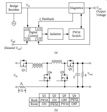
FIG. 22 Digital control concept used in SMPS with buck-and-boost mode possibilities:
(a) concept of digital control; (b) topology control; (c) compound buck-boost flowchart; (d) basic flowchart. (Source (26))
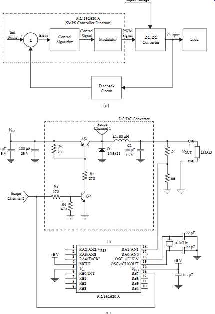
FIG. 23 Digital control in a simple buck converter design: (a) absorbing
the control function into the microcontroller; (b) circuit; (c) flowcharts.
In FIG. 22(a), the signal IL (the current in the inductors) is also fed into the digital controller, whereas input voltage is fed at another ADC input, which makes the system decide on the buck or boost requirement.
FIG. 22(c) shows the flowchart applicable to the system for the selection of the buck or boost mode and the overall power conversion-related flowchart ().
In such a system, many other aspects of overall control, such as efficiency management, diagnostics, and interactive communications with the power supply, can be easily achieved (26). Given the conceptual approach in the above example, the digital control concept in power supplies may have four different levels:
• Level I-adds simple functions that are difficult to achieve with analog components (e.g., a ramping PWM waveform for the soft-start function).
• Level II-secondary management function around a traditional analog circuit.
The digital controller monitors the output parameters and uses existing external controls to enhance the functionality of the power supply, though the control loop is still analog.
• Level III-a higher level of integration where the switcher is integrated with the microcontroller, but the implementation of the feedback loop is still analog.
• Level IV-complete digital control where all parameters are digitized and analyzed by the controller to provide appropriate outputs.
This usually requires a DSP with high-speed ADCs and PWM outputs. FIG. 23 shows the concept and implementation aspects of a digitally controlled buck converter based on a low-cost microcontroller such as the PIC 16CXXX from Microchip Technology.
FIG. 23(a) shows the concept of absorbing the control function into the digital controller. Figures 23(b) and 23(c) show the final circuit and applicable flowcharts for this pulse-skipping modulator-based design. The main and interrupt subroutines for timing generators are shown in the flowcharts.
Using a simple low-pin-count microcontroller and a suitable driver IC, a more compact digitally controlled switcher can be developed. FIG. 24(a) shows a digital power converter schematic based on a PIC microcontroller. FIG. 24(b) shows the development environment for the PIC controller, including the in-circuit debugger (ICD) (29).
For more advanced control requirements, microcontroller manufacturers such as Microchip Technology have introduced 16-bit digital signal controllers (DSCs) with DSP functionality, low pin count, and low cost. A block diagram of a typical DSC from Microchip Corp. is shown in FIG. 25(a). FIG. 25 shows the concept of implementing a synchronous buck converter, with the approximate timing involved. In such a system, sampling triggers and ADC capability are important so as not to miss critical parameters, as in FIG. 25, where asynchronous ADC sampling was used (30).
Analog comparators available within the DSC should be used for current limiting so that these comparators provide benefits that are not practicable or desirable to perform directly in the digital control loop ( FIG. 25(d)). With the cost of DSPs dropping to $2 or less, use of a DSP in the control loop is becoming a viable option (31).
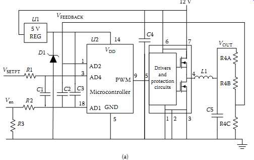
FIG. 24 A PIC microcontroller-based power converter using a half-bridge
driver IC: (a) circuit; (b) development environment.
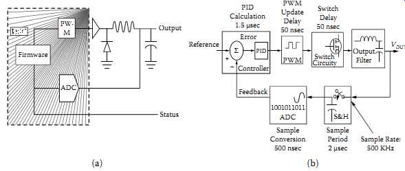
FIG. 25 Use of a digital signal controller (DSC) in an SMPS design: (a)
DSC block diagram;
(b) example of a synchronous buck implementation; (c) need for asynchronous ADC sampling;
(d) analog comparator used for current limiting outside the loop.
Caldwell (32), Kris (33), Etter and Fosler (34), Hagen and Freeman (35), and Pandola (36) provide some useful information for designing digital controllers for switching supplies, including the frequency response of the power stage (35). FIG. 26 shows a DSC-based approach for designing a full-bridge version with PFC where two DSC chips are used. Bramble and Holden (37) discuss details of a digital control system for a buck converter based on an 8051-compatible microcontroller.
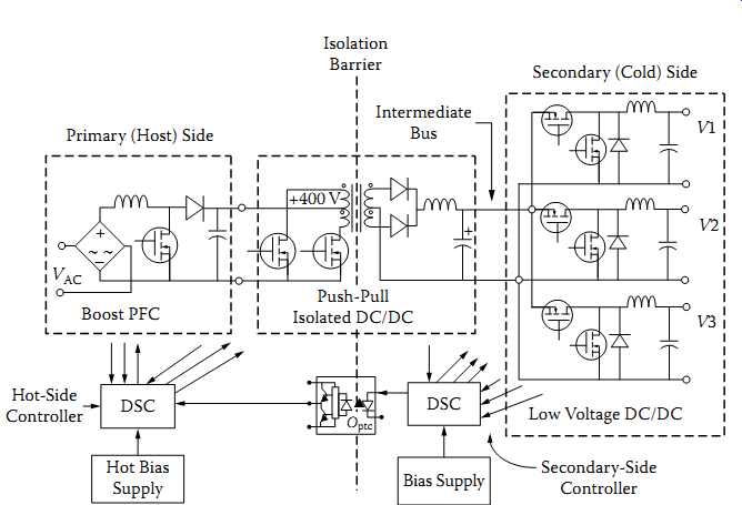
FIG. 26 DSC-based approach for PFC-based full-bridge configuration with
dual processors.
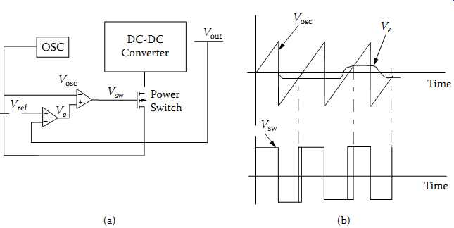
FIG. 27 Voltage-mode control: (a) block diagram; (b) associated waveforms.
9 Control Modes of Switch-Mode Converters
In developing the control circuits for a DC-DC converter, there are two important practical steps: selection of the control IC and design of the feedback loop. In this section, a brief introduction to control ICs is provided. The primary function of the control IC in a switch-mode power supply is to sense any change in the DC output voltage and adjust the duty cycle of the power switches to maintain the average DC output voltage constant. In general, an oscillator within the IC allows the designer to set the basic frequency of operation. A stable, temperature-compensated reference is also provided within the IC. There are two basic modes of control used in PWM converters:
voltage mode and current mode.
9.1 Voltage-Mode Control
This is the traditional mode of control in PWM converters. It’s also called single-loop control, as only the output voltage is sensed and used in the control circuit. A simplified diagram of a voltage-mode control circuit is shown in FIG. 27. The main components of this circuit are an oscillator, an error amplifier, and a comparator. The output voltage is sensed and compared to a reference. The error voltage is amplified in a high-gain amplifier. This is followed by a comparator, which compares the amplified error signal with a sawtooth waveform generated across a timing capacitor.
The comparator output is a pulse-width modulated signal that serves to correct any drift in the output voltage. As the error signal increases in the positive direction, the duty cycle is decreased, and as the error signal increases in the negative direction, the duty cycle is increased. The voltage mode control technique works well when the loads are constant. If the load or the input changes quickly, the delayed response of the output is one drawback of the control circuit, as it senses only the output voltage. Also, the control circuit cannot protect against instantaneous overcurrent conditions on the power switch. These drawbacks are overcome in current-mode control.
9.2 Current-Mode Control
The current control mode is a multiloop control technique that has a current feedback loop in addition to the voltage feedback loop. This second loop directly controls the peak inductor current with the error signal rather than controlling the duty cycle of the switching waveform. FIG. 28 shows a block diagram of a basic current-mode control circuit. The error amplifier compares the output to a fixed reference. The resulting error signal is then compared with a feedback signal representing the switch current in the current-sensing comparator. This comparator output resets a flip-flop that is set by the oscillator. Therefore switch conduction is initiated by the oscillator and terminated when the peak inductor current reaches the threshold level established by the error amplifier output. Thus the error signal controls the peak inductor current on a cycle by cycle basis. The level of the error voltage dictates the maximum level of peak switch current. If the load increases, the voltage error amplifier allows higher peak currents.
The inductor current is sensed through a ground-referenced sense resistor in series with the switch.
The disadvantages of this mode of control are loop instability above 50% duty cycle, a less than ideal loop response due to peak instead of average current sensing, and a tendency toward subharmonic oscillation and noise sensitivity, particularly at very small ripple currents. However, with careful design using slope compensation techniques, these disadvantages can be overcome. Therefore current-mode control becomes an attractive option for high-frequency switching power supplies. Some special problems, such as pulse-skipping oscillations, and solutions are discussed.
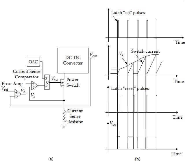
FIG. 28 Current-mode control: (a) block diagram; (b) associated waveforms.
= = =
TBL. 2 Design Constraints for a 300 MHz Pentium II Processor
Parameter Typical Value Core voltage (Vcore) 2.8 V Static voltage tolerance +100 to −60 mV Dynamic voltage tolerance ±140 mV Maximum process core current (ICC(max)) 14.2 A Typical processor core current (ICC(typ)) 8.7 A Step current slew rate 30 A/μs Input current di/dt <0.1 A/μs
= = =
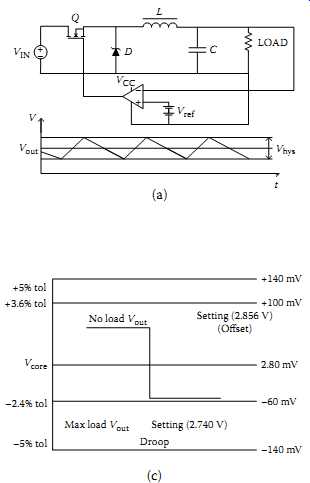
FIG. 29 Hysteretic control and a typical circuit: (a) basic concept of hysteretic
control; (b) voltage tolerance budgeting waveforms; (c) actual voltage tolerancing
for the case of the Intel VRM 8.3 specification; (d) a typical circuit.
9.3 Hysteretic Control
For processors such as Pentiums, current requirements are on the order of 20-30 A in desktops and similar systems. Other requirements are extremely low-output ripple voltages (on the order of only 50-100 mV, at most) with step load current transients on the order of 30-50 A/μs. In such situations the speed of the controller becomes very critical. TBL. 2 indicates the core voltage requirements of an old 300 MHz Pentium processor. A relatively newer technique using a hysteretic controller or ripple regulator has become prominent. Ripple regulation combines the advantages of voltage mode regulation and current-mode solutions to power supply regulation. Voltage-mode regulation is noted for reliable operation within a specified window, but it’s slow in responding to transient current demands, and loop compensation is difficult to implement. Current-mode regulation offers better transient response than voltage-mode regulation but at the expense of additional losses due to current-monitoring resistors in the circuit.
A ripple regulator responds quickly to step current demands, and it’s power efficient.
In addition, a well-designed hysteretic controller keeps the ripple-regulated VO within the specified window, maintaining general conditions required by a power-hungry CPU.
FIG. 29(a) shows the basic concept of a hysteretic-controlled buck converter that compares the actual output voltage to a reference signal corresponding to a desired output.
Within the Vhys margins set by the Schmitt trigger/comparator, the output voltage will ramp up and down. One important aspect of this approach is that the frequency of operation is not constant and depends on the input-output voltage differential, inductor value, and ESR of the output capacitor. The typical range of frequencies is from about 150 to 700 kHz. The graph in FIG. 29(a) shows the shape of the output ripple current flowing through the output capacitor. The hysteretic control concept is easy to implement, but EMI control may be difficult due to the unpredictable noise spectrum from the variable operational frequency. FIG. 29(b) shows voltage tolerance budgeting waveforms at the application of a typical load (upper waveform with no droop compensation; lower with droop compensation). FIG. 29(c) shows the actual voltage tolerances of a hysteretic control-based power supply where some offset voltages are applied above and below the nominal core voltage. In this design approach using adjustable values of offset and droop values for no-load and maximum-load conditions, respectively, variation of the output voltage is maintained within the specified limits of the processor. For example, SC1154 (from Semtech Corporation) and TPS 5211(from Texas Instruments) provide the design capabilities for the Intel VRM Spec 8.3. These controllers allow the output voltage to be adjusted from 1.3 V to 3.5 V, depending on a five-bit DAC output, which is a common requirement of VRM specifications. A guide to design calculations is available in Vosicher (41) and Nowakowski and Hodson (42). FIG. 29(d) shows a typical power supply based on a hysteretic controller such as SC1154.