AMAZON multi-meters discounts AMAZON oscilloscope discounts
...
1 Introduction
Practically all electronic systems work with DC power rails, which are usually derived from a commercial AC utility source or a limited-energy battery pack. Due to reasons related to political, environmental, and consumer pressures, saving energy, a green environment, electromagnetic compatibility, and safety aspects drive the power supply designer to be very optimistic about the overall structure of a power supply subsystem.
With more feature-packed processor-based systems becoming the norm, particularly in portable systems, multiple DC power rails are required. Another important aspect of the modern power management systems is the transient response of the power rails for load currents with fast slew rates, due to common situations such as the processors transitioning between sleep and wake-up modes.
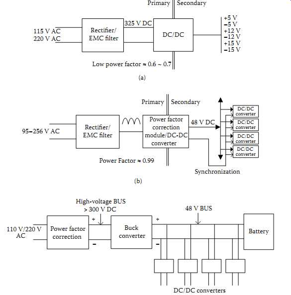
FIG. 1 Comparison of the centralized power architecture and the distributed
power architecture (DPA): (a) centralized power architecture; (b) distributed
power architecture; (c) a DPA system with 48 V intermediate bus with battery
backup.
2 Design Approaches and Specifications
A low-voltage power supply subsystem must fulfill four essential requirements: isolation from the mains, change of voltage level, conversion to a stable and precise DC value, and energy storage. In the modern world of power-hungry products with mixed power supply rail values where a battery pack or another limited-capacity alternate energy source is used as the primary or the secondary source, a few additional requirements need to be considered. These are energy-saving aspects, quality of the output with respect to fast load transients, electromagnetic compatibility issues, protection and supervisory aspects, packaging aspects, and communication interfaces.
For the power supply, the design team has two basic choices: buy or build. The final decision must consider overall cost and the time to deliver. However, when a system becomes quite complex and requires multiple power rails and critical power management, design and build becomes the choice.
2.1 Centralized Power Architecture versus Distributed Power Architecture
Traditional power distribution techniques in a system have relied on a centralized architecture where all the required power rails are derived from a single high-power switch-mode power supply (SMPS), as shown in FIG. 1(a). These conventional power supplies use an unregulated DC power supply based on a rectifier and smoothing capacitors followed by a DC-DC converter with or without power factor correction (PFC) blocks to provide different DC power rails.
The distributed power architecture (DPA) approach is to distribute power at an intermediate "medium" voltage throughout the system and convert power locally.
Distribution becomes more efficient with lower currents, and local power conversion occurs at lower power levels with the many different voltage levels required by individual circuit blocks. DPA systems are typically power factor corrected, have high efficiency (greater than 90%), and consist of a DC bus within the overall system. The selected DC bus voltage is determined by the safety requirements. Safe electrical low voltage (SELV) requires less than 60 V, and a common value for telecom systems is 48 V. FIG. 1(b) shows an example of a universal AC input (95-265 V AC) power factor-corrected DPA system with multiple DC-DC converter modules to derive individual power rail values.
Davis (1) and Curatolo (2) provide an overview of DPA concepts, including system cost aspects; Cassani et al. (3) provide some design details of a system with a 36 V intermediate bus voltage for DC-DC converter inputs. FIG. 1(c) shows a DPA system with a 48 V intermediate bus with a battery backup possibility (4). Smith (5) provides key considerations for DPA systems, and Hemena and Malik (6) provide a case for a personal computer/server situation. Several important technical considerations in the DPA approach are partitioning of the load, determining the intermediate-bus voltage value, end-to-end efficiency considerations (on the basis of AC line to load), and technology selection (2). When the overall line-to-load efficiency (LTLE) is a serious design consideration, designers should carefully account for the efficiencies of individual power supply blocks (7).
Designing power solutions for line cards in information systems that handle multiple tasks at high speeds is complex. As these boards must process large amounts of data, they incorporate multi-gigahertz microprocessors, dual-logic application-specific integrated circuits (ASICs), and other high-performance devices. These new-generation devices can require two operating voltages per chip: one for the processor core (about 2.5 V or 1.8 V and rapidly moving downward) and the other for input/output (I/O) devices, which is higher (about 2.5-3.3 V). Until recently, these power supply requirements were addressed using multiple single-output isolated DC-DC converters. However, with rising currents and declining voltages, along with tighter regulation tolerances and faster load current slew rates, multiple isolated converter solutions are not as effective in such applications. These isolated converters are not space efficient and can cause higher ohmic losses along long interconnections. Under such conditions, maintaining high overall efficiency and tight point of load (POL) regulation becomes challenging. To alleviate these issues, now there are integrated building blocks that provide DPA architecture-based solutions for POL requirements. An example from International Rectifier (part number iP1201/iP1202), where an intermediate-bus architecture (IBA) is based on an 8 V rail, is discussed in Bull and Smith (8). FIG. 2(a) illustrates the concept in this approach suitable for line cards up to about 150 W power consumption. FIG. 2(b) illustrates implementation of a POL using iP1202 (8).
2.2 Selection of DC-DC Converter Techniques
In the modern world of electronics, the three different basic approaches available for the process of DC-to-DC conversion are the linear approach, the switching approach, and the charge pump approach.
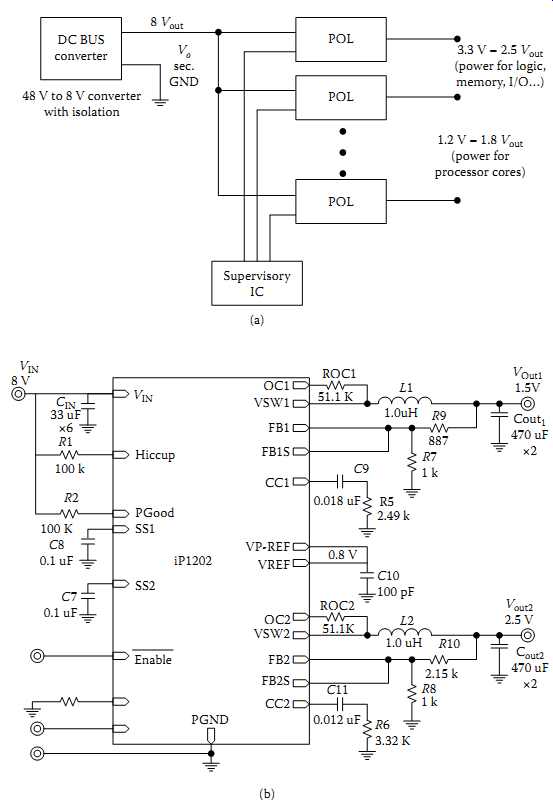
FIG. 2 An 8 V intermediate-bus architecture with 48 V to 8 V bulk converter
and POL stages: (a) concept; (b) a complete schematic for a dual-output buck
converter-based POL using iP1202.
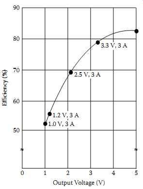
FIG. 3 Efficiency versus output voltage for a compact switching regulator
family-a typical example.
In a practical system, one can mix these three techniques to provide a complex, but elegant, overall solution with energy efficiency, effective silicon or PCB area, and noise and transient performance to suit different parts of an electronic system.
Switching-type DC-DC converters-once the clear choice for 5 V systems-suffer lower efficiency at lower voltages. In linear regulators, if the control circuits are designed with a low-power approach, efficiency is approximately given by (Vout/Vin) × 100. Compared to a high-frequency switching technique-based SMPS solution, LDO regulator ICs (or simply LDOs) are faster in responding to load current changes, produce less noise, and are more compact on a PCB or as an integrated solution for a complete silicon solution. Often, combining a switcher and an LDO makes more sense in electronic systems where the DC rail voltages are less than 5 V or 3.3 V and a combination of many different low voltages are within the same system. This is illustrated in FIG. 3, which is derived from the characteristic curves for the Power Trends PT6305 integrated switching regulators (9). The graph indicates that the efficiency drops from approximately 79% for a 3.3 V output model to 56% for a 1.2 V output device. This is mostly due to the rectification losses at very low output voltages.
Industry is continuously attempting to move forward with higher efficiencies with the switchers, by employing synchronous rectification and resonant conversion and using nonsilicon power semiconductors.
===
TBL. 1 Comparison of Popular DC-DC Converter Techniques
Feature LDOs (and) very low drop out regulators (VLDO) Charge Pump Converters Switching Regulators Design complexity Low Moderate; Moderate to high Cost Low Moderate; Moderate Noise Lowest Low; Low to moderate Efficiency Low to moderate; Moderate to high; High Thermal management Poor to moderate Good Best Output current capability Moderate Low High Requirement of magnetic parts No; No Yes Limitations Cannot step up Vin/Vout ratio Layout considerations
===
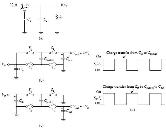
FIG. 4 Switched capacitor converters: (a) basic principle of operation;
(b) doubler; (c) inverter; (d) timing.
Charge pumps, switched capacitors, flying capacitors, and inductorless converters are all different names for DC-DC converters that use a set of capacitors rather than an inductor or transformer for energy storage and conversion. For many years, designers have used charge pumps for DC-DC conversion in applications for which the regulation tolerance, conversion efficiency, and noise specifications are not very stringent. As discussed below, these circuits use capacitors combined with switches to boost or invert the input voltage, and they don’t occupy more PCB or silicon area to implement as a single-chip converter (10). Recent generations of charge pumps have become viable DC-DC conversion methods for cellular phones, portable wireless equipment, notebook computers, and PDAs, where high-density DC-DC conversion is necessary and PCB area is at a premium (10).
In a practical system, the power supply designer has the possibility of combining these techniques. For an effective overall solution taking all specifications and cost into account, combining a large-capacity bulk SMPS in tandem with LDOs and charge pumps becomes a very effective approach. TBL. 1 provides a comparison of the three popular DC-DC converter techniques. In portable application design, the designer should be careful when selecting techniques, and in many situations the method can be a mix of the three techniques discussed.
2.3 Switched Capacitor DC-DC Converters (Charge Pump Converters)
Switched capacitor (charge pump) converters use capacitors rather than inductors or transformers to store and transfer energy. The most compelling advantage is the absence of inductors, which have greater component size, more EMI, greater layout sensitivity, and higher cost. Compared with other types of voltage converters, the switched capacitor converter can provide superior performance in applications that process low-level signals or require low-noise operation. These converters offer extremely low operating current-a useful feature in systems where the load current is either uniformly low or low most of the time. Thus for small handheld products, light-load operating currents can be much more important than full-load efficiency in determining battery life. The basic operation of switched capacitor voltage converters is shown in FIG. 4.
When the switch is in the left position, C1 charges to V1 (see FIG. 4(c)). The total charge on C1 is given by q1 = C1V1. When the switch moves to the right position, C1 discharges to V2. The total charge on C1 is now given by q2 = C1V2. The total charge transfer is given by q = q1 − q2 = C1(V1 − V2).
If the switch is cycled at a frequency f, the charge transfer per second, or the current, is given by:
I = fC1(V1 − V2) = (V1 − V2)/Req
...where Req is given by 1/fC1. The reservoir capacitor C2 holds the output constant. A basic charge pump can work as a doubler or an inverter, as shown in Figures 4(b) and 4(c), respectively. FIG. 4(d) shows the switch drive waveforms for the two cases. Some variations of the basic doubler exist for which the output voltage is about 1.33-1.5 times the Vin value (10). In some cases, output voltage can be programmed with an external resistor divider. Charge pumps can be either regulated or unregulated.
After initial charge-up transient conditions and when a steady-state condition is reached, the charge pump capacitor has to send only a small amount of charge to the output capacitor on each switching cycle. The amount of charge transferred depends on the load current and the switching frequency. During the time the bucket (pump) capacitor is charged by the input voltage, the output capacitor, Cout, must supply the load current. The load current flowing out of the Cout causes a drop in the output voltage that corresponds to a component of the output voltage ripple. Higher switching frequencies allow smaller capacitors for the same amount of droop. There are, however, practical limitations on the switching speeds and switching losses, and switching frequencies are usually limited to few hundred kHz (11).
Recent generations of charge pumps offer improved specifications and have become a viable DC-DC conversion method for many portable appliances where high-density converters are necessary and circuit area is limited. Two common charge pump types are hysteretic and fixed frequency. FIG. 5a shows the concept of hysteretic control in charge pumps. With this technique, an output voltage that falls below the reference voltage enables the oscillator. During the first clock cycle, the bucket capacitor charges to the input voltage. During the next cycle, the total charge, consisting of Cbucket and Cin, transfers to the output capacitor. This cycle repeats until the output voltage reaches the upper hysteretic threshold, at which point the comparator disables the oscillator. The internal comparator continues to enable/disable the charge pump switches based on the output level (10). The example shown is for an SC1517-5.
In a fixed-frequency type with linear regulation, shown in FIG. 5(b), the internal oscillator runs at a fixed frequency when the device is not shut down. The charge pump provides an unregulated voltage to an internal linear regulator that adjusts this voltage to a fixed output. The device achieves regulation by using an internal comparator that senses the output voltage and compares it with an internal reference while adjusting the gate drive to the internal pass MOSFET for fixed output voltage. The oscillator frequency that controls the charge pump is usually outside the sensitive frequency spectrum of cellular communication bandwidths. Unlike the hysteretic types, this type can restrict any generated switching noise to noncritical bandwidths (10).
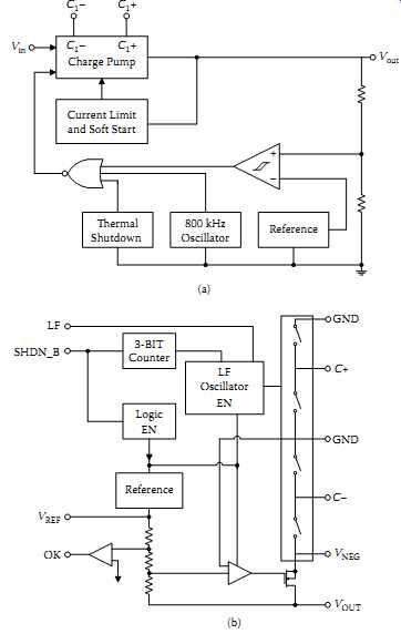
FIG. 5 Different types of charge pumps: (a) hysteretic control based; (b)
fixed-frequency type.
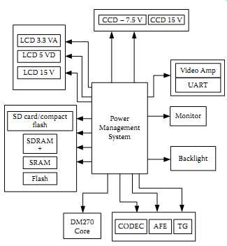
FIG. 6 Digital still camera system components.
2.4 Power Management Concepts
Modern electronic product design requires dealing with different low-voltage DC rails for the longest battery life, thermal management, EMC compliance, and PCB area optimization.
Modern multigigahertz-order processors and peripherals generate fast load current transients on their multiple DC rails, and users expect longer run times from batteries. Therefore in designing the DC power supply subsystem, one should consider the following:
• Battery pack or energy source-related aspects
• Load-partitioning aspects to minimize the number of DC rails to be used
• Dealing with power factor, harmonics, and other EMC issues
• Packaging and thermal issues
• Transient protection of the power supply and the product
• Issues related to swapping of modules
• Electrical isolation requirements
• Effects of fast transient loading at the output rails and the stability of the converter blocks
To achieve the above, designers have access to a wide variety of technologies and power management IC families, battery management techniques, architectures, and standards.
The important consideration is to deal with all of the above in an integrated manner and in a cost-effective way for a "power management solution" (15). If the overall system consumes more than 50 W with several DC rail requirements, one has to first carefully analyze the load and have an overall view of its DC rail voltages and the transient behavior of the load. Let's look at a few examples, such as a digital still camera and a cellular phone. FIG. 6 depicts the system-level block diagram of a digital still camera, based on a TMS320DM270 programmable DSP-based media processor ("DM 270") (16). The input power source for a case like this will be an Li-ion or Li-polymer rechargeable battery pack. If this particular system operates from an Li-ion battery, the input operating voltage will be from 3.6 to 4.2 V. This operating range is a critical factor in selecting the power supply topologies in the design process. In this kind of product, there are different mixes of blocks, such as the processor, memory, analog front ends (AFEs), video amplifier, motor, liquid crystal display (LCD), CCD module, and backlight for the LCD.
TBL. 2 shows each system component and its power requirements. A few concepts used in such a system include:
• DC rails for low-noise analog circuits need be separated from digital block DC rails.
• System components frequently turned on and off need to be separately powered from the continually running circuit blocks.
• 3.3 V rails (a total of eight) can be grouped into three separate sets of 3.3 V rails.
• Secure digital (SD) card memory, synchronous dynamic random access memory (SDRAM), static random access memory (SRAM), and flash memory on the DM 270 can all be powered by the same bus.
• The codec, analog front end (AFE) and video timing generator require low-noise LDOs.
• The 3.3 V rail for the LCD needs to be separated because it goes on and off during use.
===
TBL. 2 Partitioning of the System Loads
System Component Indication in Figure 3.4 Bus Voltage (V) Typical Bus Current (mA) Typical Bus Power (mW) Efficiency of an LDO-Based DC Supply (%) Efficiency of a Switcher (%) Weighted Efficiency of an LDO (%) Weighted Efficiency of a Switcher (%)
===
Appropriate supply topology selection depends on the input voltage, output voltage, noise, efficiency, cost, and space. The last three items usually compete with each other.
The first two restrict the choice of the topology. If the output voltage is always lower than the input voltage, a buck converter or an LDO will work. Otherwise, a buck-boost or a single-ended primary inductance converter (SEPIC) topology will work. A typical Li-ion battery's voltage profile varies from a high value of 4.2 V (at full charge) to 3.0 V when fully discharged. Between these limits, the battery maintains approximately 3.7 V. All selections need to be based on these values. In terms of efficiency, it’s important to consider the overall efficiency for prolonged battery life, and for this reason a special approach is to use the weighted efficiency for each power rail, as indicated in TBL. 2.
Weighted efficiency is calculated by multiplying each efficiency value by the typical bus power divided by total estimated power ratio. In real-world operation, the example here can have different modes of operation, and for each mode one has to develop a table and analyze and estimate the best options. Then it’s necessary to have an estimate of the percentage of the time the camera spends in each mode. For lower-noise considerations, even if an LDO solution is considered (in lieu of a switcher), weighted efficiency indicates otherwise for items such as the DM270_Core. For the 5 V analog bus for the video amp, low-noise operation may be mandatory, but at lower battery voltages such as 3.5 V or lower, an LDO will cease to operate. In this situation, a switcher is to be selected and then followed up with an LDO. After defining the power supply requirements, the designer can start choosing individual ICs required for the system.
FIG. 7 indicates part of the solution using a Texas Instruments TPS 65010 power management IC, which has several switcher outputs and two LDOs. In addition, a TPS 61120 IC will be required. For details, see the data sheets of the relevant ICs.
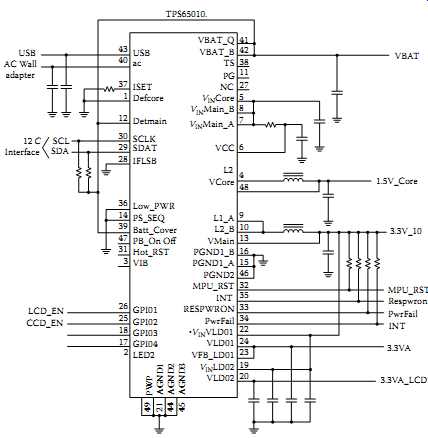
FIG. 7 Part of a power management (PM) solution for the DSC from Texas Instruments.
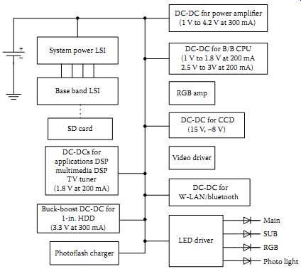
FIG. 8 Block diagram of a cellular phone in 2005 shows many low-voltage
DC supply requirements.
Let's briefly discuss the case of powering a modern cellular phone. By 2007, most cellular phones allowed many features in addition to voice communication. A trend was for cellular phones to act as MP3 players or to add a micro hard disk or a very large amount of silicon memory. FIG. 8 shows a generic block diagram of a 2005-generation cellular phone. In much older generation phones the main power rail was 3.3 V, but the newer generation chipsets use a 1.5 V main power rail because the majority of large-scale integrated circuits (LSICs) operate with voltage rails of 1.5 V or less. Examples are baseband chipsets running from 1.375 V rails and video-processing DSP chips running from 1.2 V rails. In these situations it’s possible to mix very low dropout (VLDO) linear regulators with conversion efficiencies from 80% to 90% (19). With the common acceptance of 600 mAh Li-based cell phone battery packs, and dealing with packaging problems, thermal management, and noise issues, power management of the product becomes quite critical and the designer has to make a well-informed and critically analyzed approach (19). A simple example is the case of lower than 50% efficiency of LDO solutions for converting 3.3 V to 1.8 V compared to the situation of modern-generation power rail requirements from 1.5 V to 1.2 V, which can be supported by an LDO solution with efficiencies of about 80%. For more discussion on the practical design considerations for portable wireless products, see Armstrong (19) and Maxim Integrated Products (20).
3 Specifying DC Power Supply Requirements
Let's start with the simple fact that the DC supply subsystem is expected to provide a constant set of output voltages at a maximum set of load currents. Given this requirement to be derived from an AC input rail such as 230 V/50 Hz or 120 V/60 Hz or an energy source such as a battery or a fuel cell, the designer has to start the list of specifications with input voltage, output voltages, and respective load currents. Then we can add as much secondary information as possible. The more requirement specifications we list, the easier it’s to narrow down the available options.
Design specifications act as the performance goal that the ultimate power supply must meet in order for the product to meet its overall performance specification. When developing the specification, the power supply designer must keep in mind what is a reasonable requirement and what is an idealistic requirement. Most specification-related parameters are measurable using common test setups under different environmental conditions. These specifications can be grouped into several subsets, as shown in TBL. 3.
In developing these specifications, the designer should have a clear idea of the load requirements and steady-state and transient behaviors. In a very simple case where load consumes a few watts to about 50 W in a single- or dual-rail requirement, the load can be supplied by a simple linear or switching supply where only a few of the above items need to be specified. Many complex loads require multiple rails, power management and green design concepts, transient loading conditions, tight space or weight requirements, and cost restrictions, and the designer may have to start with the generalized concept of a power supply, as in FIG. 9. In the case of an AC-powered situation, concepts in FIG. 9(a) apply, whereas for battery-powered products the concepts in FIG. 9(b) apply. Brown (21) and Rubadue (22) provide useful details on specifications and design concepts. A discussion of battery management for longest run time and standby time is presented in Section 8.
========
TBL. 3 Power Supply Specifications
Subset Item Remarks Input specifications Nominal input voltage Product is expected to work around this voltage most of the time.
Range of input voltages Product is expected to withstand this range of fluctuations.
Frequency (for AC input systems) or total energy available from a battery pack (in mAh or Ah) In the case of a battery pack, an off-the-line charger may be designed for the input frequency.
In-rush current Important for the start-up conditions.
Voltage transients Important for the reliability of the power supply and the load for reliable operation.
Permissible harmonics or power factor Governed by various standardization bodies.
Fusing Speed of fusing is based on the I 2t rating of the device.
Output specifications Nominal output voltage The load is expected to operate at this voltage.
Average and peak currents RMS values to be used.
Turn-on delay • Capacitor/inductor energy storage dependent at the time of initial switch-on.
• In multiple-rail output situations, carefully timed sequencing may be necessary.
Stability over a specified period Based on the age of the components.
Regulation specifications Load regulation • Variation of the output voltage versus current.
• Specified as a percentage or graphically shown for different input voltages.
Line regulation • Variation of the output voltage in response to changes in the input line.
• Specified as a percentage or graphically shown for different load currents.
Hold-up time Amount of time the output remains within usable limits when the input source is disconnected temporarily.
Output voltage temperature coefficient The stability of the output voltage rails. Dependent primarily on the reference source stability and the temperature tolerances of the output sampling chain resistors.
Subset Item Remarks Regulation specifications (Contd.) Transient specifications
• Overshoot, undershoot, and settling time
• Step response of the output for sudden changes of load current
• Overshoot, undershoot, etc., are dependent on the control loop behavior.
• Step response is very important in dealing with complex high-current processor loads.
Output impedance
Represents the Thevenin equivalent resistance of the power supply output.
Ripple and noise limits
These specifications may be very significant for the reliable operation and accuracy of analog- and mixed-signal circuitry.
Protection conditions
Over- and undervoltage limits at the output
These specifications indicate the safe operation limits of the load.
Output current limit Maximum load current expected.
Thermal limits
To avoid excessive temperature conditions within the product or the power supply.
Power conversion specifications
Overall efficiency In battery-powered products and green designs, this is a critical specification.
Thermal dissipation
Determines the need for cooling and packaging limitations.
Safety and regulatory agency specifications Isolation requirements
• Dielectric withstand voltage
• Insulation resistance
• For the safety of the user, a power supply should have galvanic isolation between the AC power input side and the load side.
• Insulation resistance is usually specified for the transformers involved in the design.
RFI/EMI requirements
• Conducted EMI
• Radiated RFI
• Conducted EMI specifies the line-filtering requirement.
• Radiated RFI affects the physical layout and enclosures.
Power management requirements
Energy conservation and green design aspects
Particularly important in high-power loads.
Sequencing and resetting of the output rails Critically important specification in multiple-rail situations.
===========
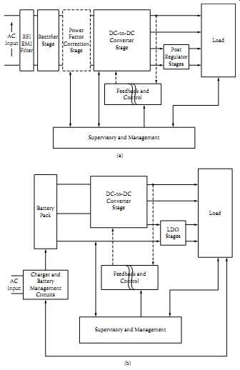
FIG. 9 Overall design approach to a complete power supply subsystem: (a)
based on an AC input source; (b) based on a battery pack with a charging subsystem.
Supervisory and Management; Charger and Battery; Management Circuits;
======
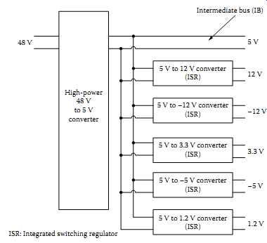
FIG. 10 ISR devices from Power Trends, Inc. in a DPA solution.
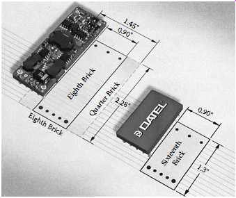
FIG. 11 Brick converter examples.
=====
4 Loading Considerations
Load connected to a power supply can be as simple as a single-rail requirement, which can be easily met by a simple linear or switching power supply. In extreme cases, the load may consist of several complex processors or other mixed-signal loads that may require multiple power rails, specialized power management aspects, and ultra-low-voltage DC rails that consume 100 A or more. Some processor loads may demand digitally controlled adjustable power rails for effective power management. In communication subsystems, the load may demand extra low-noise and low-voltage power rails. Designers should have an initial estimate of the load requirements and an idea of the nature of the load in general. The key considerations include:
• The number of voltage rails and regulation aspects
• The nature of the load transients and stability considerations
• Efficiency and power management aspects
• Protection requirements
• Noise and EMC considerations and regulatory requirements
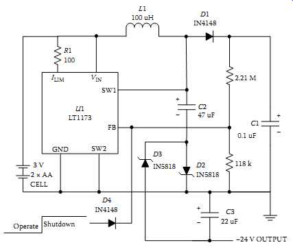
FIG. 12 Use of a boost converter IC and a charge pump to convert 3 V from
two alkaline cells to generate a +24 V and −24 V LCD bias supply.
For the simple cases of single- or dual-rail power requirements, there is a choice of three-terminal linear regulator chips; these are low cost and easy to implement, with excellent noise and drift characteristics. The most useful property is their speed of response to transient loads. The only major disadvantage of these solutions is their low efficiencies, which in general range between 30% and 50%. There are ways to improve the efficiencies of linear regulators by manipulating the rectifier circuits in the input stages using silicon-controlled rectifiers (23). Many common loads can tolerate slower responses and greater amounts of high-frequency noise. For such simple requirements, there are switching regulator solutions where the equivalent of a three-terminal linear IC solution is provided by integrated switching regulator (ISR) techniques by companies such as Power Trends. ISRs are able to provide buck, boost, or inverting voltage values from a single DC bus supply such as 5 V (24). FIG. 10 indicates a DPA solution based on an intermediate-bus architecture (IBA) of 5 V. Another fully packaged switching solution for high-current-capability DC rails is the "brick converter," where a wide range of voltages (0.9 V to 48 V) is possible at currents up to a few tens of amperes (25, 26).
FIG. 11 shows the relative sizes of quarter, eighth, and sixteenth brick sizes.
Further to examples given in Section 6.2, powering portable devices such as palm computers, pose different issues. Some of these are powered by a few AA cells from which different voltages need to be generated. The typical power source for a palm computer is a disposable alkaline cell, and using such a cell creates other design challenges, such as generating higher voltages (such as a 5 V rail from two alkaline cells of 3 V) efficiently, generating LCD bias generators (typically −24 V), and generating miscellaneous lower voltages such as 3.6 V, 2.4 V, and other values (27). In such cases, boost converters, such as the LT 1173 from Linear Technology, with charge pump configurations (to invert the +24 V to −24 V) can be used (27). See FIG. 12.
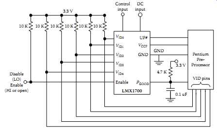
FIG. 13 A voltage regulator module under the VID command signals (four or
five bits) from the processor.
5 Powering High-Power Processors and ASICs
Advanced microprocessors and ASICs are power hungry and can consume as much as 100 A from power rails of 1.0 V or less. When the Pentium range processors entered the market in the mid-1990s (with only a few hundred megahertz clock speeds), their power consumption was a few amps to more than 10 A from voltage rails of 1.8 V to 3.3 V. In CMOS digital circuits, the power consumption is proportional to V 2, and this fact encourages chip designers to develop processors that operate with lower rail voltages (28). Two other important facts about high-end digital components are that they require multiple-rail voltages for efficiency and speed, and the load currents can have slew rates easily up to 100 A/μs. To achieve these rates, most modern high-power processors have digital command signals based on four- to five-bit code to command a voltage regulator module (VRM) to output different voltages to power the processor. This concept is shown in FIG. 13, where the processor outputs a four- or five-bit code via a special set of pins (called voltage identification (VID) pins) that command a VRM to change the voltage output from about 0.8 V to about 3.5 V in steps of 100 mV or 50 mV. For more details, see Mannion (29). The VRM is capable of adjusting its own output voltage under the command code bits from the processor within the range of values specified by the processor. An early example of this is the LXM1700 from LinFinity (29). The example in FIG. 13 is for a five-bit VID pin code from the processor. With the load demands of extremely high current slew rates, the VRM should be capable of responding quickly with low-ESR capacitors at the output. More of these design aspects are discussed in later sections. The PCB track inductances can jeopardize the required slew rate; thus designers must pay special attention to PCB layout.
To power Intel, AMD, and other high-end processors, the concept of VRMs has created a special set of power modules coming under the VRM specifications series. For details, see Brown (30), Gentchev (31), and Wong et al. (32). Most of the VRMs used on processor boards are powered by the 5 V rail of the PC power supply ("silver box").
In most processor-based systems, power rails have typical value combinations such as 1.8 V, 2.5 V, or 3.3 V, and these rails need to be properly sequenced for the reliable operation of a system. There are different possibilities of sequencing depending on the application, as shown in FIG. 14. Common themes are sequential power-up, ratiometric method, and output tracking (or simultaneous or coincidental power-up).
In sequential power-up ( FIG. 14a), the system turns on the core voltage, and when it reaches the voltage set point it turns on the second I/O rail. This technique can be used to delay the start-up of the second rail at some predetermined time after the first rail is turned on. In this technique, interlocks can be introduced, as shown in FIG. 14(d). Switching off can be based on the same principle in the reverse order. In FIG. 14(b), the ratiometric technique is shown. The two rails are turned on simultaneously, reaching regulation at their respective set points at the same time. In this method, the two rails are controlled with different slew rates. FIG. 14(c) shows the output tracking or simultaneous power-up scheme where the two rails reach their output voltages at the same rate, and once the core voltage is reached, it remains constant, while the I/O rails reach the 3.3 V value.
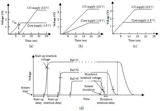
FIG. 14 Sequencing of voltage rails: (a) sequential power-up; (b) ratiometric
method; (c) output tracking (simultaneous or coincidental); (d) sequential
tracking with interlocks.
5.1 Advance Configuration and Power Interface (ACPI) Specification
In the early days of personal computing, there was no power management. Over the history of 40 years in single-chip microprocessors, power consumption has grown exponentially as evidenced by details in TBL. 4, based on Intel processors. Around 1989, Intel shipped processors with technology to allow the central processing unit (CPU) to slow down, suspend, or shut down part or all of the system platform, or even the CPU itself, to preserve and extend battery life. In 1992, an early version of PC power management techniques based on the advanced power management (APM) specification was introduced. With the need for energy saving simultaneously with the instantly available PC (IAPC), an advance version of the APM was introduced, called the advanced configuration and power interface (ACPI). The history and technical details related to this process are available in Kolinski et al. (35).
====
TBL. 4 Development of Microprocessors by Intel Processor Year Power Consumption ( Watts) Clock Frequency (MHz) Number of Transistors Feature Size of Transistors (Microns (μm))
====
TBL. 5 Comparison of Multiple Output Flyback Designs versus a POL Architecture
Feature/ Performance Multiple-Output Flyback Design POL Architecture Complexity/Component count Low Medium to high Flexibility and adaptability Rigid Easy to adapt to changing requirements Performance (general) Low Medium to high Accuracy 4-7% 1-5% Transient response Slow Fast Efficiency 70-77% 80-90% Sequencing Difficult Easy Cost Low; Low to medium Energy Star compliance Difficult Easy Regulatory approval Long Short Time to market Slow Fast
========
The ACPI specification provides a platform-independent, industry-standard approach to operating system-based power management. The ACPI is the key constituent in operating system power management (OSPM). OSPM and ACPI apply to all classes of computers, including handheld, notebook, desktop, and server machines. In ACPI-enabled systems, the basic input/output system (BIOS), hardware, and power architecture must use a standard approach that enables the operating system to manage the entire system in all operational situations. From a computer power system designer's viewpoint, ACPI power management means generating and managing a multitude of voltages on the motherboard and riser cards with no user intervention to enable the processing of audio, video, and data streams. ACPI-compliant computers require the generation of these multiple voltages at various current ratings as the system transitions between sleep states.
The ACPI defines six possible discrete system operating states, which are referred to as S0 to S5, in order of highest to lowest power consumption. For more details on the ACPI and ACPI power controllers, see Kolinski et al. (35) and Lakkas and Duduman (36).
5.2 Multiple-Output Power Supplies versus Point of Load (POL) Approach
Traditionally, the approach for a multiple-rail output requirement was a multirail switching supply based on a multiple-winding high-frequency transformer. A classic example of this approach is in the desktop computer power supply (known as the "silver box"), where a transformer-isolated forward-mode topology is used. In modern devices such as set-top boxes, many higher-voltage rails are also required, in addition to the usual 3.3 V, 2.5 V, 1.8 V, 1.5 V, and other lower-DC rails (37). Traditionally such requirements can be fulfilled by utilizing an off-the-line flyback power supply. However, in powering set-top boxes and similar systems, flexibility, Energy Star compliance, power sequencing, and other attributes can be easily approached by a point of load (POL) regulation, compared to a traditional multirail output approach based on flyback design. TBL. 5 compares these two approaches from a designer's viewpoint.
A POL solution for a system such as a set-top box is easily developed starting with an off-line converter, an intermediate-bus voltage (IBV) such as 12 V, in addition to a core supply of 3.3 V or similar. Then using the IBV the designer can combine efficient synchronous converters, ordinary switchers, LDOs, inverters (positive to negative rail converters), or charge pump type converters. A typical example is shown in FIG. 15.
Using the concepts discussed above, many new single-chip power management solutions have started coming into the marketplace.
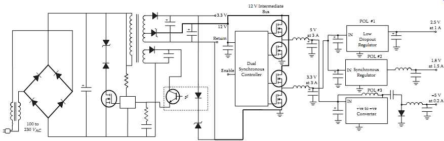
FIG. 15 POL design approach suitable for set-top boxes and similar devices.
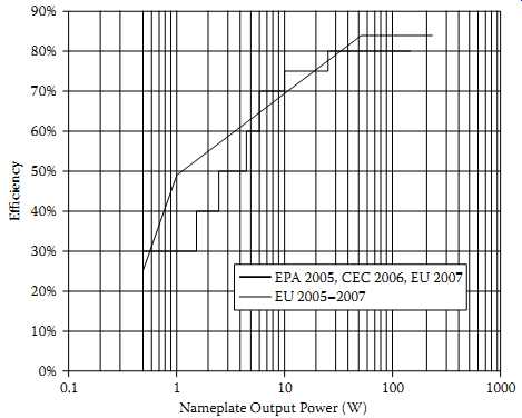
FIG. 16 Efficiency requirements for external power supply curves based on
CEC, EPA, and EU recommendations.
5.3 External Power Supplies and New Energy Standards
For certain types of consumer products, by using an external or a wall plug-in supply, designers can gain board space, eliminate a major source of heat, and reduce EMI noise. In addition, this may even provide the option of freeing the designer from the burden of getting safety approvals for the product. Until the late 1980s, wall plug-in supplies were limited to less than 25 W, but as of 2005 this capability has grown to about 250 W. Most low-power, older versions were linear regulator based, but recent energy-saving and related standards worldwide have pushed these products to adopt switch-mode designs. It’s important for designers to note the recent standards released by the California Energy Commission (CEC), Environmental Protection Agency (EPA), and European Union (EU) regarding efficiency requirements and the nameplate output power ratings, as summarized in FIG. 16. For more details on external power supplies, international power converter requirements, and recent energy-saving standards, see ___.
In the latter part of 2009, regulators in the United States and EU have been busy proposing new minimum efficiency standards for off-the-line power supplies. This mostly covers external power supplies such as mobile phone chargers. Around 70% of minimum acceptable efficiency during device operation, as well as 250-300 mW of no-load dissipation, expected by these regulatory bodies is currently met by the industry. By 2011 the European Commission is expected to lower the no-load dissipation down to 150 mW.
One difficult target may be the 30 mW no-load consumption limit agreed upon by LG Electronics, Motorola, Nokia, Samsung, and Sony-Ericsson. TBL. 6 summarizes the future scenario of efficiency targets based on these "star-ratings." Five stars mean a 30 mW no-load consumption, the hard target to achieve in the near future.
===
TBL. 6 New Star Ratings and the No-Load Consumption of Chargers
No Load Consumption Limits No of Stars Less than 30 mW *****
30 mW to 150 mW ****
150 mW to 250 mW *** 250 mW to 350 mW ** 350 mW to 0.5 W * ≥.5W No stars
===
Power management chip design companies are currently spending heavy on R&D efforts to achieve these regulatory requirements by introducing new ICs and measurement techniques. One example is in (43). Another example of optimizing magnetic for the AC-DC adaptors with Energy Star is detailed in (44).
5.4 Load Switches and Switching Off Parts of the Power Supply Rails
With manufacturers and consumers both trying to be conscious of energy conservation, particularly for standby power (sometimes called the vampire power), switching unused parts of the circuits has become very common in portable products. In order to achieve this under processor control, various load switches have been introduced by power component manufacturers.
5.5 PM-Bus and Digital Control Protocol for Power Converters
Over the last 10 years many board designers have moved to intermediate-bus architecture (IBA) discussed in the early parts of the Section. This is due to processor-based products, particularly the portables, as well as large systems such as data center power units that have multiple on-board DC-DC converters to generate the diversity of power rails needed by different silicon devices. With many power supply manufacturers and IC houses launching digitally programmable POL converters, a common control bus and an open-standard architecture for power converter control was required. As a result power management bus (PMBus) architecture was proposed in the early part of the new millennium, with a fully defined command language and a transport and a physical interface. The protocol was founded by a coalition of power supply and semiconductor manufacturers, and in 2005 revision 1.0 of the protocol was placed in the public domain. Development of the protocol and the promotion of the standard was transferred to a special interest group known as the System Management Interface Forum.
PMBus is not a standard for AC-DC power supplies or DC-DC converters. It only facilitates communication with a power converter or another device. The PMBus transport layer is based on the Version 1.1 of the system management bus (SMBus) (discussed briefly in Section 8), which is based on the industry favorite I2C bus. A typical bus implementation is shown in FIG. 17(a). It uses the wired-AND connection of all devices on the bus to provide arbitration in the event of bus contention, and it’s electrically similar to the I2c bus. Its master device is not based on proprietary silicon.
PMBus communications are based on a simple command set as depicted in the summary of FIG. 17(b). Every packet contains an address byte; followed by a command byte; zero, one, or more data bytes; and an optional packet error code (PEC). More details are in (46). FIG. 17(c) depicts the flexibility of the PMBus specification, in power supply control parameters. It summarizes the conceptual view of how these commands are used. PMBus usage in power converter units in data centers allows better efficiency and power management for optimal control of energy usage.
FIG. 17 PMBus protocol and connections: (a) PMBus bus-master connections
to POL converters; (b) typical host to salve information transfer; (c) command
settings allowed.)