AMAZON multi-meters discounts AMAZON oscilloscope discounts
...
1. Introduction
The basic theory of the switching power supply has been known since the 1930s. Practical switch-mode power supplies (SMPSs) have existed since the 1960s, starting with components designed for other uses and thus poorly characterized for SMPS use. Early SMPS systems were running at very low frequencies, usually from a few KHz to about 20 KHz.
Early SMPS designs justified the SMPS techniques for higher output power ratings, usually above 500W.
Toward the mid-1980s most SMPS units were available for much lower power ratings with multiple output rails, while oscillator frequencies were reaching the upper limit of 100 KHz. Today most switchers operate well above 500 KHz, and newer techniques allow the systems to run at several MHz, making use of new magnetics, surface mount components, and the resonant conversion techniques. The rapid advancement of microelectronics in the last two decades (1975-1995) has created a necessity for the development of sophisticated, efficient, lightweight power supplies that have a high power ‑ to ‑ volume (W/in^3) ratio with no compromise in performance. The high ‑ frequency switching power supply meets these demands. Recently it has become the prime powering source in the majority of modern electronic systems. The trends associated with the switch-mode power supplies for the electronic products and systems are (a) reaching direct off-the-line design approach, (b) utilizing higher frequencies, (c) increasing output rating/volume, (d) minimizing the components, and (e) increasing reliability.
2. Building Blocks of a Typical Off-the-Line Switching Power Supply
FIG. 9(a) depicts the basic block diagram of a typical off-the line SMPS. This block diagram depicts the AC line RFI filter block, the supervisory and power management blocks, and the requirement of I/O isolation in the overall system. (Note the isolation indicated in the feedback and control block, which is essential for this purpose.) The EMI/RFI filter can be either part of the power supply or external to it, and it’s generally designed to comply with national or international specifications, such as the FCC class A or class B and VDE-0871. Within the past two decades, because of the emphasis placed on power quality issues, power factor correction (PFC) as applicable to the nonlinear behavior of the input current waveform of a rectifier has become an important issue. For power supplies with output capacities greater than 75 W, PFC is mandatory in some jurisdictions.
Input/output isolation is essential to off-the-line switchers. The isolation used within different stages may be optical or magnetic, and it should be designed to comply with Underwriters Laboratories (UL)/Canadian Standards Association (CSA) or Verband Deutscher Electronotechniker (VDE)/International Electrotechnical Commission (IEC) safety standards. The UL and CSA require 1000 V AC isolation voltage, whereas VDE and IEC require 3750 V AC. Consequently, any step-down power transformer or high frequency switching transformer within the DC-DC converter stage has to be designed to the same safety isolation requirements.
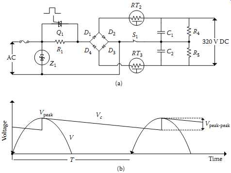
FIG. 1 Input section of an off-the-line power supply: (a) overall arrangement;
(b) ripple voltage calculations.
3. Rectifier Section
In older linear power supplies, a step-down transformer was used with low-voltage rectifier circuits. In off-the-line switching power supplies, a line voltage capability rectifier set is used directly off the AC line without any low-frequency line isolation transformer between the AC mains and the rectifiers. Because in most of today's electronic equipment the manufacturers are generally addressing an international market, power supply designers must use an input circuit capable of accepting many different line voltages, normally 90 to 130 V AC or 180 to 260 V AC. FIG. 1 shows such a circuit using a voltage doubler technique. When the switch S1 is closed, the circuit may be operated at a nominal line of 110 V AC. During the positive half cycle of the AC, capacitor C1 is charged to the corresponding peak voltage, approximately 160 V DC, through diode D1.
During the negative half cycle, capacitor C2 is charged to 160 VDC through diode D4.
Thus the resulting DC output is the sum of the voltages across C1 + C2, or 320 V DC.
When the switch is open, D1 to D4 form a full-bridge rectifier capable of rectifying a nominal 230 V AC line and producing the same 320 V DC output voltage. In many universal input systems, there is an automatic changeover capability built into the design.
Two important aspects of the representative circuit in FIG. 1(a) should be noted.
One is the energy storage in capacitors C1 and C2. The other is the resistor R and special components such as negative temperature coefficient (NTC) thermistors for the purpose of inrush current limiting. FIG. 1(b) illustrates the simplified case of a half-wave rectifier where the charging and discharging of the capacitor is simplified by a sawtooth assumption for the discharge during the negative half of the AC cycle. During this process, approximate average DC output voltages for the half-wave or full-wave cases are given by …)
where VRMS is the RMS AC input voltage, I_load is the average load current, f is the line frequency, and C is the value of the effective smoothing capacitor. The RMS ripple voltage is given by…
V I fc ripple rms load …
(Half wave)
V I fc ripple rms load
(Full wave)
For more details, see Smith (1, 2). It’s important to note that the above equations are based on a simplified approach only, and a more accurate and detailed treatment is available elsewhere (3).
For diodes, maximum forward rectification current capability, peak inverse voltage (PIV) capability, and the surge current capability (to withstand the peak current associated with turn-on) are the most important specifications. Proper calculation and selection of the input rectifier filter capacitors are very important, because this will influence performance parameters such as low-frequency AC ripple at the output power supply and the holdover time. Normally, high-grade electrolytic capacitors with high ripple current capacity and low ESR need to be used with a minimum working voltage of 200 V DC. Resistors R4 and R5 ( FIG. 1(a)) provide a discharge path when the AC supply is switched off.
3.1 Fuses
Even the selection of the fuse for the input section needs to be done based on proper specifications. Fuses are categorized by three major parameters: current rating, voltage rating, and, most important, "let-through" current, or I2t rating. The current rating of a fuse is the RMS value or the maximum DC value that it must exceed before blowing.
The voltage rating of a fuse is not necessarily linked to the supply voltage. Rather, the fuse voltage rating is an indication of the fuse's ability to extinguish the arc that is generated as the fuse element melts under fault conditions. The voltage across the fuse element under these conditions depends on the supply voltage and the type of circuit. For example, a fuse in series with an inductive circuit may see voltages several times greater than the supply voltage during the clearance transient.
The I2t rating of a fuse is defined by the amount of energy that must be dissipated in the fuse element to cause it to melt. This is sometimes referred to as the pre-arcing let-through current. To melt the fuse element, heat energy must be dissipated in the element more rapidly than it can be conducted away. This requires a defined current and time product. The heat energy dissipated in the fuse element is estimated in wattseconds (or joules), or I 2Rt for a particular fuse with an internal resistance of R. As the fuse resistance is a constant, this is proportional to I 2t, normally referred to as the I 2t rating for a particular fuse or the prearcing energy. The I2t rating categorizes fuses into the more familiar slow-blow, normal, and fast-blow types. It should be noted that the I2t energy can be as much as 20 times greater in a slow-blow fuse of the same DC current rating. For example, a 10 A fuse can have an I 2t rating ranging from 5 A2s for a fast fuse to 3000 A2s for a slow fuse. The selection of fuse ratings for off-line SMPSs is discussed by Billings (4). For high-power semiconductors such as power diodes and transistors, manufacturers indicate a value of I2t, from 10 ms (for 50 Hz) or 8.3 ms (for 60 Hz), that should not be exceeded. Comparing this value with the fuse I2t permits us to verify the protection.
3.2 Inrush Current Limiting
An off-the-line switching power supply may develop extremely high peak inrush currents during turn-on unless it incorporates some form of current limiting in the input section. These currents are caused by the charging of the filter capacitors, which at turn-on present a low impedance to the AC lines, generally limited by the ESR plus the total input resistance within the charging path. If no protection is employed, these surge currents may approach very large values to blow the input fuses.
Several methods are widely employed in introducing a high impedance to the AC line at turn-on. FIG. 2 illustrates a few common methods. In FIG. 2(a), an NTC thermistor limits the inrush. Initially, the thermistor resistance is high, which limits the inrush. As the inrush current flows through the thermistor, it heats up and the resistance decreases for normal operation. FIG. 2(b) indicates a power semiconductor (MOSFET)-based technique. The FET limits the inrush by turning on slowly as its gate capacitor charges. FIG. 2(c) shows an approach using a resistor and a relay.
The input filter charges through the resistor until the relay is commanded to connect the filter to the converter and short the resistor. Each of these has its advantages and drawbacks (7). FIG. 1(a) illustrates the combination of thermistor and series power semiconductor (such as a triac)-based techniques, which is very popular in computer power supplies.
One of the self-limiting techniques is to use an input inductance to limit inrush current, as in FIG. 2(d). This filter implements the required damping using inductor L2 and resistors R1/R2 in parallel to the main DC-carrying inductor L1. The value of L1 is typically 5 to 10 times larger than L2. More details of this technique are discussed by Bell (7), giving attention to the design of the magnetics.
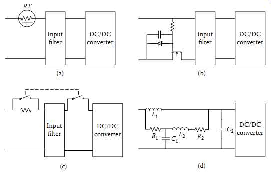
FIG. 2 Power supply in-rush current limiter techniques: (a) thermistor technique;
(b) MOSFET-based approach; (c) resistor relay; (d) inductor based.
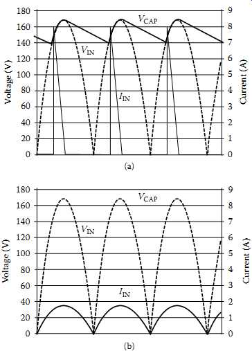
FIG. 3 Input current and voltage relationships of a rectifier stage such
as in FIG. 1(a):
(a) case of a typical rectifier without PFC; (b) ideal full-wave rectified PFC case with PF = 1.
3.3 Power Factor Correction Blocks
Power factor correction aligns the current waveform with the input voltage waveform.
If the waveforms are not aligned, the power factor (PF) is less than 1; if they are aligned, the PF is unity. FIG. 3 illustrates this. FIG. 3(a) illustrates a typical non-PFC case where the nonsinusoidal current waveform does not align with the voltage waveform.
FIG. 3(b) illustrates the case of a half-sinusoidal input current waveform with PF = 1.
In most cases, PF-corrected designs can achieve PF values of 0.95-0.98, and supplies that are not corrected can have a PF that is significantly less, usually less than 0.65.
Given this simple explanation, it’s also necessary to appreciate the case of nonsinusoidal rectifier currents, which can generate many harmonics of the line frequency waveform.
When a repetitive waveform is not sinusoidal, it generates many harmonics, and the total harmonic distortion is given by:
... where V1 to Vn are the fundamental and the harmonics of the voltage waveform. VTHD is the ratio of all harmonics (added on an rms basis) to the fundamental.
Only current and voltage components with the same frequency can produce nonzero active power. In practice, sometimes it’s reasonable to assume that the input voltage waveform is purely sinusoidal, despite any distortions in the current waveform.
Under such an assumption, V, the RMS voltage of the input waveform, is approximately equal to the RMS of the fundamental component, V1, and we can get the approximate relationship
.... where I1 is the in-phase fundamental RMS current and I is the total RMS current. With this discussion, we can appreciate the regulatory bodies defining the limits of harmonics generated by electrical systems connected to the AC utility grid. The EU put into effect EN 61000-3-2 to establish limits on harmonics up to 40th harmonic of the AC line-powered equipment's input current. Amendments in 2001 clearly state that PCs, PC monitors, and TV receivers with power ratings from 75 to 600 W must have PFC power supplies.
In practical cases of off-line SMPS systems, the fundamental idea is to use a power MOSFET switch and an inductor in the series path of the charging capacitor to artificially align the voltage and charging current waveforms. For the case of a boost converter configuration, this can be achieved as shown in FIG. 4(a), where the smoothing capacitor is now shifted toward the DC-DC converter stage. A power factor control IC that switches the MOSFET at higher frequency smooths out the current waveform and aligns its fundamental component with the input voltage waveform.
Several IC manufacturers, such as Fairchild, Microlinear, and International Rectifier, supply various controller ICs for PFC or PFC/PWM combo operations. Figures 4(b) and 4(c) are typical configurations in a boost converter topology (8) based on Fairchild parts FAN 752B and FAN 4803. It’s important to note that the main smoothing capacitor C_in has now moved further toward the DC-DC converter stage. For the case of discontinuous conduction, such as the case of using a FAN 752B-type controller for outputs up to 200 W, the boost converter's MOSFET turns on at zero inductor current and turns off when the current meets the desired input reference voltage. FIG. 4(d) indicates the waveforms in discontinuous mode.
Sandler et al. (9), Valentine (10), and Section 9 of Kularatna (11) provide a practical overview of PFC techniques and application information. Some new PFC techniques are discussed later.
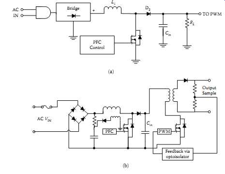
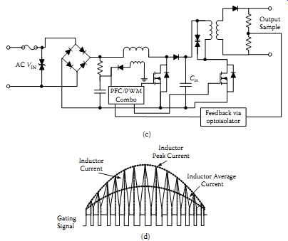
FIG.
4 Practical approach to power factor correction: (a) basic concept of implementation;
(b) use of a stand-alone PFC controller IC; (c) use of a PFC/PWM combo IC
in a boost topology; (d) waveforms in discontinuous mode.
4 Popular Transformer-Isolated Configurations for Off-the-Line Power Supplies and Industry Approaches
Most off-line AC-DC converters offer universal input voltage capability that typically spans 90-265 V AC at 47-63 Hz frequency range. This wide range allows configuration free use anywhere in the world, for portable devices. This concept relieves the designer from the concern that end users may incorrectly set their equipment.
However, this condition of universal input range may create problems in selecting fuses, as at lower input the voltages converter may draw much higher current for the same output power.
Given the above condition, all off-line systems should have one safety-related condition:
keeping the output DC loads isolated from the AC mains input. Given the direct rectification-based bulk DC power supplies used in compact systems, this isolation is provided only by a transformer-isolated DC-DC converter topology. In maintaining this isolation criteria, and the total wattage of the output loads, most off-line power supplies are based on transformer-isolated forward-mode converters, and the flyback topologies.
For example , in situations such as the silver box of a desktop computer, where most high current rails are 3.3 or 5 V, mixed with small-capacity 12 V rails, a forward-mode design is used. However, in systems such as set-top boxes and the like where voltage rails of up to 33 V are used, a flyback topology is selected. FIG. 5 indicates typical cases of forward mode designs and flyback designs used in common off-line power supplies.
For many applications where only 5 V and ±12 V are required by the load, a multirail output AC/DC converter is used, without any intermediate DC-DC converter stages, or POL converters. Some of these units are adhering to Energy Star and other similar regulatory guidelines (16). For compact AC-DC adapters, where weight and the size is important, monolithic off-line switchers are used. An example is TOPSwitch family from Power Integrations (17). For future-generation GSM cell phones and the like, universal AC wall adaptors with four-star efficiency ratings are expected. The aim is to ensure the mobile industry adopts a common format for mobile-phone chargers for overall reduction of standby consumption up to 50%.
Another common industrial requirement is to have battery backup within the off-line power supply. In this case (which is different from an external battery charger (AC adaptor) supplying an internal battery inside a portable product) a DC bus is used with a bidirectional charger based on a charge-discharge algorithm. A typical example is shown in FIG. 6.
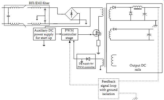
FIG. 5 Simplified block diagrams of off-the-line switch-mode power supplies:
(a) a forward mode case similar to desktop computer power supply; (b) flyback-type
design suitable for set-top boxes. (Part (b)
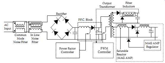
FIG. 6 Typical magnetic component usage in off-line SMPS systems.
5 Magnetic Components
5.1 Transformers and Inductors
Magnetic elements are the cornerstone of all switching power supply designs but are also the least understood. There are three types of magnetic components inside switching power supplies:
• Forward - mode transformers
• Flyback- mode transformers
• Inductors such as AC filter inductors, DC filter inductors, or magnetic amplifiers Each has its own design approach. Although the design of each of these magnetic components can be approached in an organized step ‑ by ‑ step fashion, it’s beyond the intent of this Section. For further information, Brown (20) is suggested.
5.1.1 Magnetic Materials:
Magnetic materials can be divided into three broad categories, each with its own distinct range of characteristics and capabilities:
- 1. Magnetic metals and alloys, in tape or laminated form (e.g., silicon steel, mumetal, permalloy, amorphous metals)
- 2. Powdered magnetic metals (e.g., "powdered iron," moly permalloy powder)
- 3. Magnetic ceramics, or ferrites
5.1.1.1 Magnetic Metals:
Typically these have a high saturation flux density (7-23 kG) and a high permeability.
Electrical conductivity is also high, requiring their use in laminated or tape form to reduce eddy current loss. A large range of shapes is available, limited primarily to "two-dimensional" shapes by the wound tape or laminated construction. The high flux capability makes them most suitable as line frequency (50-400 Hz) transformers and inductors. Eddy current losses limit use at high frequency, although some find application up to several hundred KHz.
5.1.1.2 Powdered Metals:
These are magnetic metals that are powdered, coated with an insulator, and pressed and sintered to shape. Eddy currents are reduced by the small particle size, extending the useful frequency range to a few megahertz in some applications. The insulated particles create a distributed air gap, giving these materials a low permeability, typically in the range of 8-80, with values to 550 obtainable in moly permalloy powder (MPP). The low permeability and a tolerance for DC current make these materials suitable for filter inductors at medium frequencies (typically 1-100 kHZ).
A relatively stable and well-defined permeability allows them to be used for nonadjustable tuning inductors, with a typical tolerance of a few percent. Saturation flux densities are typically in the range of 5-10 kG, but a very gradual saturation characteristic limits the maximum flux when inductance variations must be minimized. Available core shapes tend to be limited; toroids are the most common, with "E" cores, pot and cup cores, and a few similar shapes also available in some materials.
5.1.1.3 Ferrites:
Ferrites are dark gray or black ceramic materials. They are very hard, brittle, and chemically inert. Most common ferrite materials such as MnZn and NiZn exhibit good magnetic properties below Curie temperature (Tc). Ferrites are characterized by very high resistivity, making them the most suitable material for transformers and inductors operating at high frequencies (up to tens of MHz) when low loss or high Q is of major concern. Saturation flux densities are low, in the 2-5 kG range, with permeabilities in the middle range of a few hundred to 15,000. Ferrites have the widest range of available core shapes, including any of the shapes for the other materials. Maximum linear dimensions are limited to a few inches by standard fabrication processes, although large cores can be assembled in sections.
The flexibility in shape often makes ferrites the material of choice, even when their other desirable properties are not required. They can easily be magnetized and have a rather high intrinsic resistivity. These materials can be used up to very high frequencies without laminating as is the normal requirement for magnetic metals.
NiZn ferrites have a very high resistivity and are therefore most suitable for frequencies over 1 MHZ, but MnZn ferrites exhibit higher permeabilities (μi) and saturation induction levels (Bs). Different kinds of power ferrite material are available from many vendors. FIG. 6 indicates the typical block diagram of an SMPS with magnetic components.
A usage summary is indicated in Section 4 of (11).
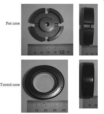
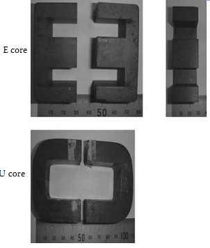
FIG. 7 Common core types used in power supplies. Pot core Toroid core E
core U core
5.1.2 Core Geometry and Common Core Materials:
Cores come in many shapes and sizes. The three most common core types are shown in FIG. 7. There are many more types, but they are all based upon these basic styles.
Some of the important considerations when selecting a core type are core material, cost, the output power of the power supply, the physical volume the transformer or inductor must fit within, and the amount of RFI shielding the core must provide. Core material considerations are summarized in Section 4 of (11).
===
TBL. 1 Power Ferrite Materials from Phillips: Their Usage and Frequency Characteristics
Material Grade Characteristics Usage Available Core Types
3B8 Medium frequency (<200 kHz) Small power transformers and general-purpose transformers RM, P 3C80 Low frequency (<100 kHz) Power transformers in TV applications E, EF, ETD, EC, U 3C10 Low frequency with improved saturation level Flyback transformers U 3C85 Medium frequency (<200 kHz) Industrial use E, EF, ETD, EC, RMP, EP, Ring core 3F3 High frequency (up to 1 MHz) Resonant power supplies E, EF, ETD, RM, P, EP, Ring core 3F4 High frequency (1-3 MHz) Resonant power supplies
===
A few examples of the commonly used core materials in modern switching power supplies are F, K, N, R, and P materials from Magnetics Inc.; 3C8 and 3C85 from FerroxCube Inc.; and H7C4 and H7C40 materials from TDK. These ferrite materials offer low core losses at operating frequencies between 80 kHz and 2.0 MHz. TBL. 1 indicates the available power ferrite materials from Phillips, their usage, and their characteristics.
Resonant power supplies make it possible to exploit the area beyond 1 MHz, which requires power ferrite transformers with useful properties in the 1-3 MHz frequency range. Meeting this need is a newer power transformer core material, 3F4, MnZn ferrite.
The chemical composition includes dopants to reduce the hysteresis loss and high frequency wall damping loss. The material also suppresses electrical conductivity and thus the eddy current losses.
5.1.3 Winding Techniques and Practical Considerations:
The design and winding technique used in the magnetic component's design has a great bearing on the reliability of the overall power supply. Two situations arise from a poor transformer design: high-voltage spikes are generated by the rate of transitions in current within the switching supply, and the possibility of core saturation can arise during an abnormal operational mode. Voltage spikes are caused by a physically "loose" winding construction of a transformer. When the windings are physically wound distant from one another, the leakage inductances store and release a portion of the energy supplied to a winding in the form of voltage spikes. It also delays the other windings from seeing the transition in the drive winding. Spikes can cause the semiconductors to enter avalanche breakdown, and the part can instantly fail if enough energy is applied. It can also cause significant RFI problems.
A snubber is usually the solution, but this lowers the efficiency of the power supply.
Core saturation occurs when there are too few turns on a transformer or inductor. This causes the flux density to be too high, and at high input voltages or long pulse widths, the core can enter saturation. Saturation is when the core's cross-sectional area can no longer support additional lines of flux. This causes the permeability of the core to drop, and the inductance value to drop drastically.
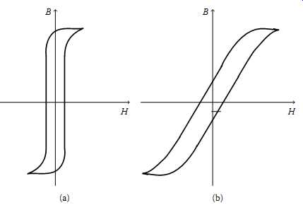
FIG. 8 B-H loop for a tape-wound core: (a) ungapped; (b) gapped.
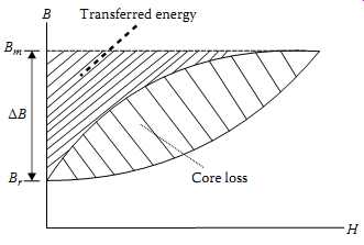
FIG. 9 B-H curve required for a flyback power supply.
5.1.4 Forward-Mode and Flyback Transformers:
For forward-mode operation, transformers may use either tape-wound cores or ferrite cores. Tape-wound cores are used at the lower frequencies because their high flux density required and the tape thickness must be reduced, both of which increase the core cost.
This makes the tape-wound core more costly than ferrites at frequencies over 10 kHz.
Tape-wound cores often have to be gapped with a minimal-type air gap. FIG. 8 shows the hysteresis loop of a typical tape-wound core both with and without an air gap. Because the loop is extremely square, any unbalance in the switching process could cause saturation for some part of the cycle, thus generating extra losses in the circuit and distorting the output. As indicated in FIG. 8(a), the gapped core will require a large difference in transistor currents before it will saturate the core.
One other method to eliminate this problem of core saturation is to use a composite core. These cores are made with an ungapped tape-wound core surrounded by another tape-wound core containing a small air gap. Composite cores avoid the problems of unbalanced transistors and also reduce or eliminate spikes in the output. In state-of the art power supplies running at frequencies over 200 KHz, where the losses could be high, ferrites are the dominant core material because of their lower cost and availability of variety of shapes and sizes.
5.1.4.1 Flyback Transformers:
The transformer cores for flyback circuits require an air gap in the core so that they don’t saturate from the DC current flowing in their windings. As mentioned above, the tape-wound core and ferrite core can both be provided with air gaps. The toroidal permalloy powder core is also used because it offers a distributed-type air gap. The frequency of the unit will dictate the selection of either tape-wound cores or ferrites as described previously, while the powder cores will operate at frequencies up to 50 kHz.
Operation of the flyback converter is based on the storage of energy in the core and its air gap during the on time of the switch and discharging the energy into the load during the switch's off time. The magnetic core operates in one quadrant of its B-H curve. For high-energy transfer in a small volume, the core should have the B-H curve shown in FIG. 9. An ideal core has a large available flux swing (ΔB), low core losses, relatively minimizes the transformer size. As the frequency increases, high-frequency materials are low effective permeability, and low cost. MPP cores, gapped ferrites, Kool Mμ, and powdered iron cores are used in this application.
In the case of ferrites, to increase their energy transfer ability ferrites must have an air gap added into the core's structure ( FIG. 10). Although the air gap increases the energy transfer of the ferrite core, it can create EMI problems. Better-shielded core shapes, such as pot cores, PQ cores, RM cores, and EP cores, are used to combat stray magnetic flux emitted from the air gap. The disadvantage of these shapes is higher cost.
5.1.5 Inductors:
The switching regulator usually includes one or several power inductors. Because of the large DC current through its windings, the core must have a large air gap to keep it from saturating. Cores used here are gapped ferrite cores, permalloy powder cores, and high-flux powder cores. In the current waveform, because there is usually only a small ripple, the AC flux swing in the core is small. Therefore powdered iron cores and silicon laminations may also be used. They are less expensive than the above-mentioned cores but have much higher losses, and therefore care must be taken in the design of such units to avoid overheated inductors and possible damage that may be caused to other components.
Ferrite E cores and pot cores offer the advantages of decreased cost and low core losses at high frequencies. For switching regulators, F or P materials are recommended because of their temperature and DC bias characteristics. By adding air gaps to these ferrite shapes, the cores can be used efficiently while avoiding saturation.
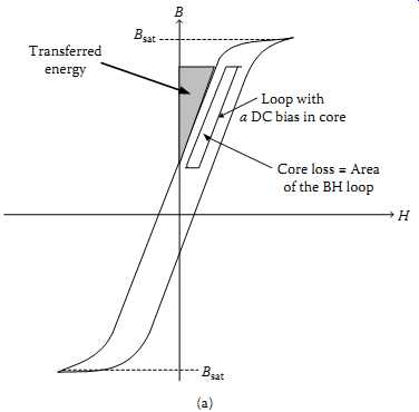
FIG. 10 Effect of gap in ferrite core: (a) ungapped ferrite; (b) gapped
ferrite. Transferred energy; Core loss = Area of the BH loop; Loop with
DC bias in core
5.2 Planar Magnetic
The concept of planar magnetics has existed for many years; however, the idea gained popularity in the late 1990s due to its low-profile configurations. The windings consist of either copper spiral turns on single- or double ‑ sided printed circuit boards or stamped, flat copper foil windings.
The windings are separated from each other and the core by thin sheets of Kapton or Mylar insulation. When necessary, they are separated by special plastic bobbins to maintain safety specifications. These assemblies are available in a fully encapsulated form to meet certain military specifications.
Advantages of the planar construction include low-profile configuration (e.g., high efficiency, lightweight, and uniform construction) and high power density (e.g., low manufacturing times and high frequencies of operation). Some disadvantages include high costs of design and tooling for printed circuit boards and special ferrite cores, inefficient means of terminating windings to the board, and thermal temperature rise of magnetics.
Another approach to planar magnetics is the multilayer circuit board, a more condensed configuration. The primary and secondary windings are stacked vertically on different layers of a circuit board with a thin film of FR4 separating them. The multilayer circuit board offers all the advantages of the planar configuration and provides an even lower-profile transformer. An additional advantage of the multilayer build is that heat is transferred out of the transformer more efficiently so that thermal rise is not as much of a problem compared to single- or double-layer types.
5.2.1 Planar Magnetics and New PWM ICs:
With the distributed power architectures being widely adopted by the industry, new D/CMOS PWM ICs, combined with integrated PCB transformers, allow simple flyback, and forward converters to operate at frequencies up to 1 MHz, with performance similar to zero-switching topologies.
An example of such an IC is Si 9114 from Siliconix Inc..
Planar transformers can be more efficiently used if the subsystem is viewed as an entire unit that includes the power supply and the load. Usually the load is some type of digital circuit and will include a microprocessor and memory, as well as custom-designed ASICs. System complexity has so increased that many designers are now using multilayer printed circuit boards where six and even more layers have become common.
These systems can now utilize a "free transformer" directly in the PC board as shown in FIG. 11. Magnetics Inc. provide practical details related to magnetic materials and cores used in switch-mode power supply systems.