AMAZON multi-meters discounts AMAZON oscilloscope discounts
...
Introduction
The concept of resonance based on an LC tank circuit has long been used in high power systems for generating sinusoidal voltage and current waveforms for testing and easy switching purposes. However, due to its circuit complexity it had not been widely employed in low-power DC-DC converter design until about the early 1990s. The thrust toward resonant power supplies has been fueled by the industry's demand for miniaturization, high-power efficiency, as well as low EMI.
Resonant converters are based on soft-switching techniques, which turn on and turn off semiconductor switches in a switch power supply at either zero-voltage or zero-current crossings, namely zero-voltage switching (ZVS) and zero-current switching (ZCS) respectively.
During the switching period, if either the voltage or current is zero, the switching power loss would be zero. Thus the converter can operate at a high frequency without causing high switching losses, and therefore the heat sinks may be reduced or even eliminated for low-power applications. Moreover, high-frequency operation would reduce the size of reactive components needed in the converter; as a result the power density can be increased on top of the power efficiency improvement. Also, ZVS and ZCS involved in the resonant converter operation can greatly reduce dv/dt and di/dt compared to hard switching converters, thereby reducing the switching stresses and EMI associated.
Fundamentals of Resonant Converters
Because there are no natural zero crossings existing in a DC power supply, no matter what techniques are used, zero-voltage or zero-current crossings have to be generated to achieve soft switching of semiconductor switches. Circuit resonance based on LC is widely used for this purpose; therefore the terms resonant converters and soft-switching converters can often replace each other without changing the meaning.
In a broader sense, soft-switching conditions can be satisfied at the power source side, at the semiconductor itself, or at the load side. In fact, a mains power supply has natural zero-voltage crossings, which have been used to create a natural ZVS condition for thyristors in traditional controllable rectifiers, so strictly speaking soft switching may be achieved using an AC link without circuit resonance. However, in a DC-DC converter application there is no such luxury unless a resonant DC-link is specially created; therefore circuit resonance has to be used.
Resonant converters for DC power supplies can be roughly categorized into resonant switch converters and load resonant converters according to where zero-voltage or zero-current soft-switching condition is created. Depending on whether it is a full resonance or partial resonance, they can also be categorized into full-resonant converters and quasi-resonant converters.
=====
TBL. 1 Possible Ways that ZVS and ZCS ON and OFF Can Be Achieved
Turning ON Turning OFF Method ZVS! (Needs care) ZCS? (not sure)
ZVS (Yes, V ~ 0)
ZCS? (not sure) A parallel capacitor ZVS? (not sure)
ZCS (Yes, I ~ 0)
ZVS? (not sure) ZCS! (needs care) A series inductor
~ZVS (V ~ 0) ZCS (not sure)
~ZVS (V ~ 0) ZCS (not sure) A parallel clamping diode in conduction ZVS? (not sure)
ZCS (I = 0)
ZVS? (not sure)
ZCS (I = 0)
A series-blocking diode in discontinuous current mode
=====
Soft-Switching Mechanism
Depending on the condition of zero-voltage switching or zero-current switching, resonant converters are often called ZVS converter or ZCS converters. Actually switching involves switching on and switching off, which can make the situation more complicated.
TBL. 1 summarizes how ZVS or ZCS can be achieved regardless of what specific technique is being used.
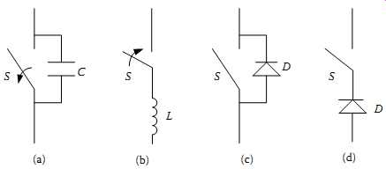
FIG. 1 Soft-switching configurations of an active power switch: (a) parallel
capacitor; (b) series inductor; (c) parallel diode; and (d) series diode.
FIG. 1 indicates the conditions in TBL. 1 as applicable to a switch in a resonant converter circuit, and the four possible soft-switching mechanisms are explained below:
1. Using a capacitor in parallel with the active switch to achieve ZVS OFF. This is because the capacitor voltage was zero when the switch is ON, and it cannot change simultaneously when the switch is turned OFF. So the voltage remains close to zero during the switching-off period, which is particularly true for modern semiconductor switches as they have a very fast switching time, and therefore quasi ZVS OFF is achieved. However, special care has to be taken to ensure the voltage across the switch is zero (normally by resonance, which will be discussed later) to turn the switch ON, otherwise shorting would occur, which may cause damage to devices. When a parallel capacitor is used, the current flowing through the switch is determined by the circuit and the actual switch used, so it is not sure whether ZCS ON and OFF are achieved.
2. Using an inductor in series with the active switch to achieve ZCS ON. This is because the inductor current was zero when the switch is OFF, and it cannot change simultaneously when the switch is turned ON. So the current remains close to zero during switching-off period, and therefore quasi ZCS ON is achieved.
However, special care has to be taken to ensure the current flowing through the inductor is zero to turn the switch OFF, otherwise overvoltage would occur, which may cause damage to devices. When a series inductor is used, the voltage across the switch is determined by the circuit and the actual switch used, so it is not sure whether ZVS ON and OFF are achieved.
3. Using a diode in parallel with the active switch to achieve approximate ZVS ON/ OFF during the diode conduction period. This is because when the diode is on, its voltage is clamped to its forward on voltage drop, which is small, so quasi ZVS ON and OFF of the active switch can be achieved. The actual current flowing through the switch may be zero because some switches, such as BJTs, cannot conduct negative current through it, or it can be a value sharing with the diode if the switch has bidirectional conductibility like some MOSFTETS.
4. Using a diode in series with the active switch to achieve ZCS ON/OFF in discontinuous mode. This is because the diode blocks the current flow in a discontinuous mode. There would be no current flow, so ZCS ON and OFF can be achieved.
It should be noted that the above analysis is based on ideal active switches. In a practical circuit design, the switch parasitic parameters and conductivity may need to be considered. For example, ideally the power losses at ZCS ON is zero, but practically MOSTETs can have large parasitic output capacitances, which can cause large turning on losses at high frequencies. The actual current and voltage across a switch may be zero or a value sharing with the blocking diode depending on the voltage-blocking capability of the switch.
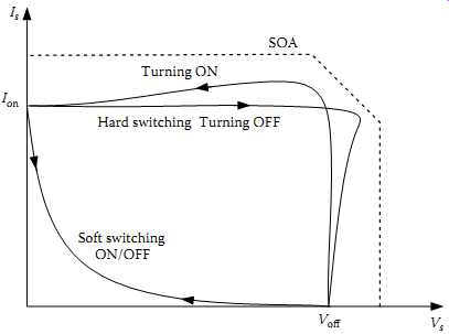
FIG. 2 Comparison of voltage-current trajectories of hard switching and soft
switching
===
TBL. 2 Comparison of Soft-Switching Resonant Converters to Hard-Switching Converters
Advantages Disadvantages
Low switching losses, heat link may not be needed
More component counts to create zero-voltage or current conditions Low switching stress and EMI
High voltage and/or current ratings for components
High power density due to reduced heat generation and high operating frequency
Complicated main circuit and controller design; parasitic parameters often need to be considered
===
Comparison between Hard-Switching and Soft-Switching Converters
It is well understood that if hard-switching techniques such as PWM are used, the losses in power switches and EMI can be very high, particularly at high frequencies.
Soft-switched resonant converters demonstrate clear advantages in these areas, which lead to new converters with high-power efficiency and high-power density. However, because resonant converters are involved in zero-voltage or -current creation and accurate control of switching at these points, both the main circuit and controller become complex, and often more components are needed; therefore a higher level of understanding and expertise is required from the designer. Also, due to the resonance, normally the peak voltage or current values are higher than their PWM counterparts, which increases the V/I ratings of the devices.
FIG. 2 illustrates typical voltage and current trajectories of hard switching and soft switching of a power switch. When the switch is on, its voltage is almost zero, and the current is Ion; when it is off, the current is zero and voltage is V_off. It can be seen that during the hard-switching period, both the voltage and current are high, so the switching power losses can be very large. Overvoltage at switching off and overcurrent at switching on often occur, and it is important to ensure both the on and off trajectories stay within the safe-operating area (SOA) of the switch, otherwise the switch may fail. If the switch is ideally soft switched with either ZVS or ZCS, the switching power losses would be zero. In practice, it cannot be exactly zero but is much lower than hard switching.
A general comparison between hard-switching converters and soft-switching resonant converters is listed in TBL. 2.
Resonant DC-DC Converters
Resonant-SwitchDC-DC Converters
The basic structure and operating principal of resonant-switch power converters is no different from traditional hard-switching DC-DC converters. The major change is that LC components are used to resonate at certain periods to offer ZVS or ZCS conditions for the semiconductor switches, so they become "resonant switches." Depending on the number and configuration of the LC pairs in relation to the active switch and diode, many different types of ZVS and ZVS converters can be configured.
FIG. 3 shows eight possible topologies using only one inductor and one capacitor as a pair of resonant components by Luo and Ye [1]. They also showed 38 possible resonant topologies if three resonant components are used, and 98 for four components. In principle all these configurations may be used in resonant converter design, which can lead to many topological variations of resonant-switch buck, boost, and buck-boost resonant converters. In practice, only simple configurations are used.
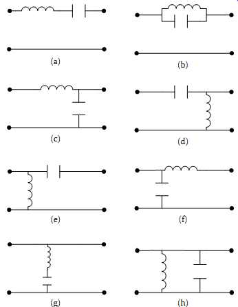
FIG. 3 Eight topologies using two resonant components.
Figures 4 and 5 show two typical ZCS DC-DC buck converter and ZVS DC-DC buck converter circuits respectively. Fundamentally quasi ZCS ON is achieved utilizing the series inductor Lr, and ZVS OFF using the parallel resonant capacitor Cr. The resonance between Lr and Cr generates zero-current and zero-voltage conditions so that ZVS ON and ZCS OFF can be achieved. In practical operation the circuit resonance and zero crossings can be affected by load and parameter variations, so special attention has to be given in designing both the main circuit and controller to ensure that soft-switching conditions are satisfied; otherwise overvoltage or shorting can occur, which may cause damage. Because the resonant period is more or less fixed with given Lr and Cr, the output voltage is regulated by changing the switching frequency [2-3].
Even very simple resonant-switch ZCS or ZVS converters can have many different topological variations. For example, if the series diode Da in FIG. 4 is changed to be in parallel with the switch, the circuit would still be able to operate with ZCS, but the current would be in a full-wave mode rather than half-wave; and although the advantage of the converter shown in FIG. 5 is that the parasitic capacitance of the active switch S can be used advantageously as part of the resonant capacitor Cr, other ZVS configurations exist that can bring in other advantages.
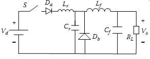
FIG. 4 A ZCS resonant-switch buck converter.
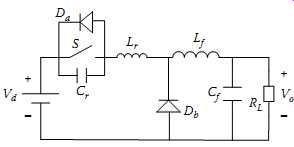
FIG. 5 A ZVS resonant-switch buck converter.
===
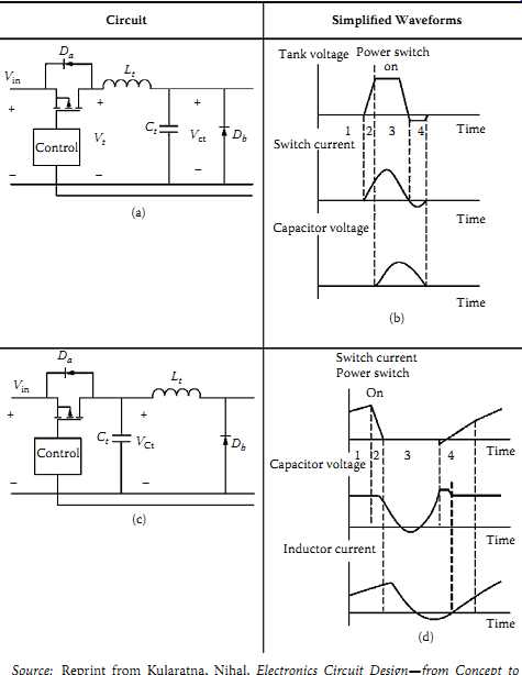
TBL. 3 Comparison of ZCS and ZVS, Quasi-Resonant, Buck Converters, Circuit; Control
Switch current; Tank voltage; Capacitor voltage; Time; Power switch; Simplified
Waveforms
===
TBL. 3 shows another two ZCS and ZVS quasi-resonant buck converter examples and compares their basic operation. In the case of ZCS, assume in period 1 the load current (not shown in the diagram) is freewheeling through the diode Db; when the switch is turned ON in period 2, the current flowing through it increases but remains to be very low, so quasi ZVS ON is achieved. After the inductor current reaches the load current in period 3, the diode stops conducting, so Ct and Lt begin to resonate. After the inductor current resonates to zero, the switch can be turned off with ZCS. The diode Da actually starts to conduct after the current changes the direction, which offers an ideal switching condition. When the resonant voltage across Ct becomes zero, the diode Db starts to conduct, and the circuit repeats another switching cycle. In the case of ZVS, assume the power switch is on initially and the DC input voltage is applied to Ct and Db. Because the voltage across Ct cannot change instantaneously, in Period 2 the switch can be turned OFF with quasi ZVS. In period 3, diode Db starts to conduct, and Ct and Lt start to resonate.
In period 4, when the voltage across Ct swings back to Vin, the voltage across the power switch becomes zero, so ZVS ON can be achieved. Similar to the situation in ZCS, the body diode Da would also be conducting, offering an ideal switching condition. After the power switch turns on, the inductor current would increase, Db would turn off, and the circuit gets ready for the next switching cycle.
In both the cases the resonant frequency is determined by Lt and Ct, although the parasitic parameters of the switch and diode can make the situation more complicated.
Half-Bridge ZVS Resonant Converter Design Example
The TEA1610 produced by Philips is a monolithic integrated circuit controlling for a zero-voltage transition resonant converter. There are two packages available: DIP16 (plastic dual in-line package, 16 leads, 300 mil, long body), and SO16 (plastic small outline package, 16 leads, body width 3.9 mm, low stand-off height). The IC can drive two power MOSFETs in a half-bridge configuration. It also includes a level-shift circuit, an oscillator with accurately programmable frequency range, a latched shut-down function, and a transconductance error amplifier [5]. The circuit enables a broad range of applications for different input voltages up to 600V. It is suited to TV and monitor power supplies well. The block diagram of TEA1610 is shown in FIG. 6.
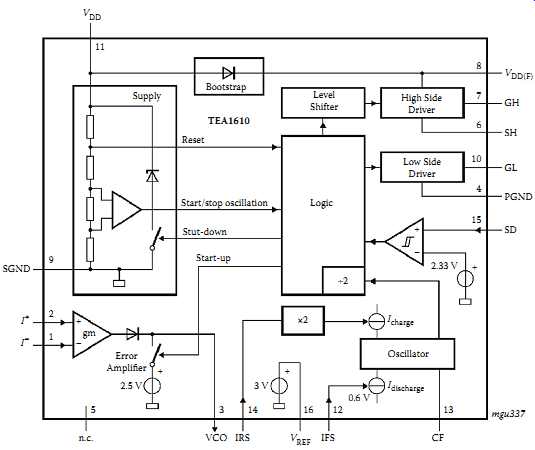
FIG. 6 Block diagram of TEA1610 ZVS controller.
TEA 1610 can be used to control a half-bridge ZVS resonant power supply using a basic configuration as shown in FIG. 7. A more detailed circuit diagram is shown in FIG. 8. At the main circuit side, the half bridge is connected to a series resonant tank consisting of Lr, Cr, and the output, which is series loaded via a transformer with a central tap at the secondary side. A conventional center-tap full-wave rectifier is used to provide a DC output in this example, although other rectifier configurations are acceptable.
The leakage inductance of the transformer can be used as the resonant inductance, so the transformer is often purposely designed to have a large leakage. If the leakage inductance is not large enough, then an external inductor has to be used as shown in the diagram. The parallel capacitor Cp in parallel with the lower-side power switch is to achieve quasi ZVS OFF, and it resonates with Lr and Cr when the switch is off, so that zero-voltage switching ON condition can be created. Once the voltage across the switch becomes negatively biased, its body diode would turn on, offering a favorable switching condition. Although there is no capacitor directly connected to the high side of the switch, effectively there is a capacitance across it by the input DC power supply pass.
There is no direct zero-voltage detection to ensure ZVS, so the resonant circuit and the control range have to be carefully designed to ensure the system can operate safely in the defined load range. The output voltage is monitored, and the controller automatically varies the switching frequency in a closed loop to maintain it to be constant.
TEA1610 has high- and low-side gate drive capability using a bootstrap capacitor. At start-up, after the applied voltage reaches the nominal value of VDD, the low-side power switch is turned-on, and the high-side power switch remains in the nonconducting state.
This start-up output state guarantees the initial charging of the bootstrap capacitor (C_boot in FIG. 8) used for the floating supply of the high-side gate drive. During start-up, the voltage on the frequency capacitor (Cf) is zero, which defines the start-up state. The output voltage of the error amplifier is kept constant (typically 2.5 V) and switching starts at about 80% of the maximum frequency when pin VDD reaches the start level. The start-up state is maintained until VDD reaches 13.5 V, the oscillator is activated, and the converter starts operating.
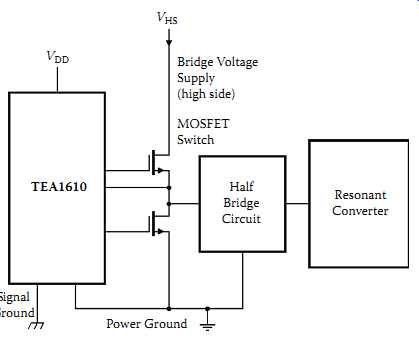
FIG. 7 Basic TEA1610 configuration.
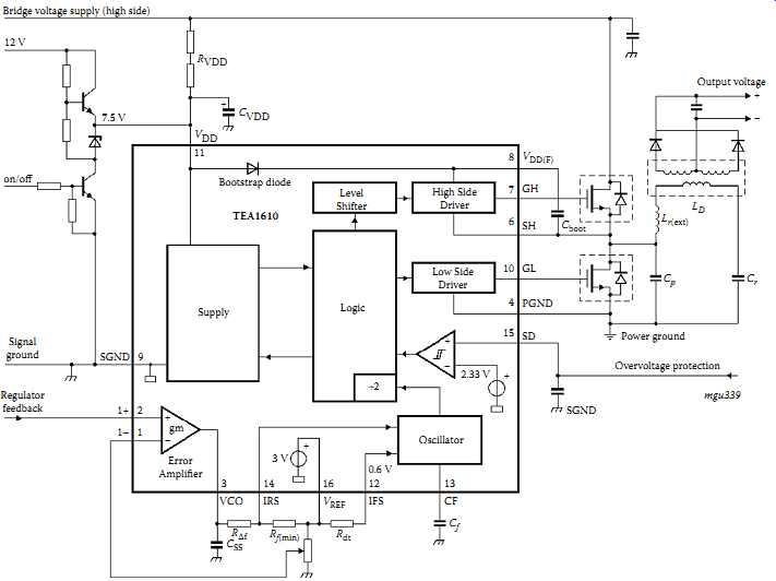
FIG. 8 TEA1610 design example. Bridge voltage supply (high side)
The internal oscillator is a current-controlled oscillator that generates a sawtooth output. The frequency of the sawtooth is determined by the external capacitor Cf and the currents flowing into the IFS and IRS pins. The minimum frequency and the dead time are set by the capacitor Cf and resistors Rf(min) and Rdt. The maximum frequency is set by resistor RΔf. The oscillator frequency is exactly twice the bridge frequency to achieve an accurate 50% duty ratio, which is fixed during the operation. The error amplifier is a transconductance amplifier. Thus the output current at pin VCO is determined by the amplifier transconductance and the differential voltage between input pins I+ and I-. The output current IVCO is fed to the IRS input of the current-controlled oscillator.
The source capability of the error amplifier increases the current in the IRS pin when the differential input voltage is positive. Therefore the minimum current is determined by resistor Rf(min), and the minimum frequency setting is independent of the characteristics of the error amplifier. The error amplifier has a maximum output current of 0.5 mA for an output voltage up to 2.5 V. If the source current decreases, the oscillator frequency also decreases, resulting in a higher regulated output voltage. During start-up, the output voltage of the amplifier is held at a constant value of 2.5 V. This voltage level defines, together with resistor RΔf, the initial switching frequency of the TEA1610 after start-up.
The shutdown (SD) input has an accurate threshold level of 2.33 V. When the voltage on input SD reaches 2.33 V, both power switches switch off immediately, and the TEA1610 enters shutdown mode.
During shutdown, pin VDD is clamped by an internal zener diode at 12.0 V with 1 mA input current. This clamp prevents VDD rising above the rating of 14 V due to low supply current to the TEA1610 in shutdown mode. When the TEA1610 is in the shutdown mode, it can be activated again only by lowering VDD below the VDD (reset) level (typically 5.3 V). The shutdown latch is then reset, and a new start-up cycle can commence.
===
Load Power Converter Power M Conditioner Track Loop Pick-up coil
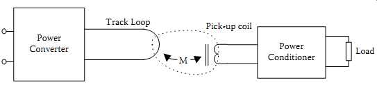
FIG. 9 A basic IPT power supply.
===
Load Resonant Converters for Contactless Power Supplies
Introduction to Inductive Power Transfer
The main objective of an inductive power transfer (IPT) system is to transfer power from a static track loop to some galvanically isolated "pickup" circuits over a large air gap so that wireless/contactless power transfer can be achieved. The air gap gives much freedom to the mechanical movement of secondary power "pickups" but makes IPT a very loosely coupled system. In a practical situation, the track "wire" may be very long while the magnetic "pickup" coils may be quite short so that the actual coupling coefficient can be as low as typically 1% or less, compared with about 95%-98% for transformers and 92% for induction motors [6]. To transfer power from the primary track loop to the secondary pickup coil across an air gap, a high-frequency alternating magnetic field linking the primary and the secondary as illustrated in the dotted line in FIG. 9 is required.
Therefore a power converter is necessary to generate a high-frequency AC current along the track loop. Because the induced voltage in a pickup coil is normally unsuitable to be used directly, a power conditioner is usually needed to maximize the power transfer capacity and regulate the pickup voltage, normally to a constant DC, to drive the load.
The main purpose of the primary converter is to invert a DC voltage (if it is an AC source, normally it is rectified into DC first) into a high-frequency AC current to generate a high-frequency magnetic field. Because the track loop or coil is normally large and exposed to the outside for easy coupling to the secondary power pickups, the EMI has to be low, which means the current waveform needs to be very good. This, together with the high power efficiency requirement, makes resonant converters desirable for wireless power supply applications.
Because an IPT system has an inherent track inductor and requires high-quality track current waveforms, load resonant converters that utilize the resonance of the track resonant circuit are normally the simplest and most economical choice. When a power pickup circuit is coupled with the primary track inductor, its impedance can be reflected back and modeled as a whole resonant tank. And at the secondary side, the pickup circuit is tuned and rectified to provide a contactless/wireless power supply.
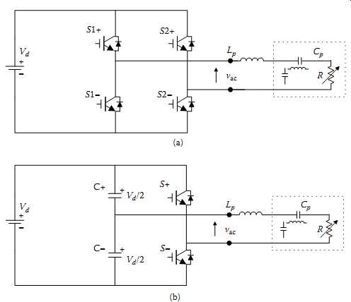
FIG. 10 Voltage-fed resonant inverters: (a) full bridge; (b) half bridge.
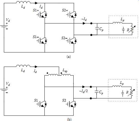
FIG. 11 Current-fed resonant inverters: (a) full bridge; (b) half bridge.
Voltage-Fed and Current-Fed Resonant Converters Topologies
A voltage-fed DC-AC converter/inverter has two basic topologies: full bridge and half bridge, as shown in FIG. 10. The switching network of the full-bridge topology has four switches, whereas two of these switches are replaced with two suitably large capacitors in a half-bridge topology. As the voltage changes across these capacitors are negligible under steady-state conditions, they serve as voltage sources with half the magnitude of the DC power supply. Therefore the maximum voltage output of the half-bridge inverter is ±Vd/2 compared to ±Vd in the full-bridge topology. The frequency, magnitude, or phase of the output voltage of a voltage-fed switching converter may be controlled with power switches at their gates. A dead time (also called blanking time) between the turn-on and turn-off of each pair of switches in the same leg is necessary in order to avoid the shorting of the voltage source producing a "short through" failure in the switching devices. The minimum duration of the dead time is determined by the on and off delays of the switching devices, plus a safety factor.
Theoretically, a current-fed resonant converter is the dual of the voltage-fed resonant converter. However, practically there is a big difference. This results from the fact that a current source cannot stand alone naturally like a voltage source without using superconductivity or a closed-loop control. For economic reasons, a large inductor is normally put in series with a voltage source to form a quasi-current source as shown in FIG. 11. As the current flowing through the inductor is nearly constant at high frequencies under steady-state conditions, it appears like a current source. However, this inductor and voltage source configuration increases the system order and can cause dynamic problems requiring special circuit control and protection methods.
Similar to voltage-fed resonant converters, a full-bridge topology and a push-pull current-fed topology with a phase-splitting transformer dividing the DC current are shown in FIG. 11. There are not many differences in the performance of these two topologies; for example, the latter does not require isolated high-side gate drives and doubles the resonant voltage.
Analogous to the protection required to avoid shorting of the voltage source in voltage-fed converters, here the current source must not be broken to avoid the occurrence of high overvoltages. Therefore at least one leg has to be on over the whole period of operation. However, because the switching devices normally turn on faster than they turn off, practically there may be no need to design an overlap time in gate drives of normal switching devices.
A very important aspect needing special attention in the design of voltage- or current fed inverters is the connection between the switching network and the resonant tank. Because two voltage sources cannot be connected in parallel arbitrarily due to the possibility of shorting the sources, the output of a voltage-fed inverter should not be connected to a voltage-source type of load such as a pure capacitor branch. In consequence, a voltage-fed switching network normally matches series-tuned (or series parallel tuned with a series branch in the beginning) types of resonant tanks with at least one inductor being series connected at the input port as illustrated in FIG. 10.
Similarly, for a current-fed inverter, as two current sources cannot be placed in series arbitrarily due to the possibility of creating overvoltage problems, the output of a current fed switching network should not be connected to a current source type of load such as a load comprising inductive branches only. Thereby, the current-fed inverting network normally matches parallel-tuned (or parallel-series-tuned with a parallel branch first) resonant tanks with at least one capacitive branch connected at the input port as illustrated in FIG. 11. In the above two situations, a series- or parallel-connected resistor at the input port will also do, but they are seldom used in practice since this introduces high power losses.
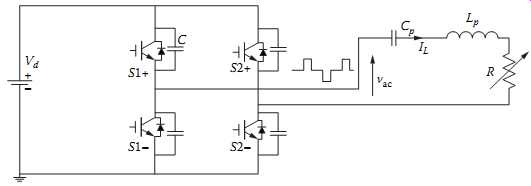
FIG. 12 A voltage-fed series resonant power supply.
A Full-Bridge Voltage-Fed Resonant Converter
As discussed earlier, voltage-fed converters have two basic configurations: a full-bridge topology using four switches and a half-bridge topology where two switches from the full bridge are replaced by two large capacitors. Due to the price drop of the semiconductor switches, the full-bridge topology becomes more popular. FIG. 12 shows a typical full-bridge voltage-fed series resonant converter for use in IPT applications. It comprises a DC voltage source Vd, an inverting network comprising four switching devices in a full bridge, and a series-tuned resonant tank. The track coil is modeled as a lumped inductor Lp, and the load is represented by an equivalent resistor R. A series capacitor Cp is used to tune the track depending on the track length. In a practical application, Cp may be distributed at certain positions along the track so as to limit the maximum voltage on the track. The four capacitors in parallel with the switches are used for soft-switching purposes as will be discussed later. The parasitic output capacitances of the switches are combined into these four capacitors so they are utilized advantageously.
Unlike a current-fed resonant converter whose output AC voltage is mainly determined by the average DC input voltage under ZVS conditions, the output voltage of a voltage-fed inverting network is completely under the control of the switching devices of the inverting network. In consequence, the track current can be regulated by duty cycle control. One control strategy is to shift the phase of the gate signals. In FIG. 12, the switches S1+ and S1-, S2+ and S2- are complementarily controlled. That is, when S1+ is "on," S1- is "off"; similarly, when S2+ is "on," S2- is "off," and vice versa. If both the upper switches S1+ and S2+ (or both the lower switches S1- and S2-) are "on," the AC output voltage from the inverting network is zero. Otherwise, the output voltage will be either positive Vd or negative Vd, depending on the state of the switches. Because of this, phase-shift duty cycle control can be utilized to regulate the output voltage and consequently the track current. FIG. 13 shows a situation when the gate signals of S2+ and S2- are lagging S1+ and S1- by 120°. In this case, the output voltage is a PWM square wave with a duty cycle of 2/3. It is obvious that if S1+ (S1-) and S2+ (S2-) are completely in phase, i.e., the phase shift is zero, the output voltage will be zero. On the other hand, if the switching is completely out of the phase, i.e., the phase shift is 180°, then the output voltage reaches its maximum value with a fundamental magnitude (RMS) given by:
V = 4 / x sqr-rt 2 Vd
…where Vd is the DC input voltage.
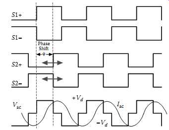
FIG. 13 Phase shift control.
In a more general case where the phase shift angle φ is between 0° and 180°, this voltage can be expressed as:
…where D = φ/π is the duty cycle of the output voltage. A duty cycle of 2/3, corresponding to a phase shift of 120º, is a preferable operating point where the harmonic distortion is the lowest for a square waveform output.
====
PI Resonant Tank Track Current Track Current Detection and Processing
Iref Vac Inverting Network Phase Shift
+ Gate Control -
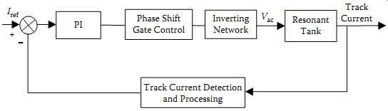
FIG. 14 Closed-loop output track current regulation.
====
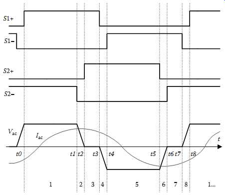
FIG. 15 Soft-switched waveforms of a voltage-fed series resonant converter.