AMAZON multi-meters discounts AMAZON oscilloscope discounts
...
In a practical circuit, because the switching devices turn off more slowly than they turn on, a dead time is necessary to prevent momentarily short-circuiting the DC voltage source. Therefore a blanking-out period exists so that the actual PWM phase shift control range is slightly larger than 0º and smaller than 180º. As a result, the maximum output voltage is slightly smaller than the ideal value given in Equation (1).
To achieve a constant track current output, a closed-loop control (shown in FIG. 14) is normally used. A current sensor such as a toroidal current transformer or an LEM device can be used to measure the instantaneous track current. As the measured current changes with time at a relatively high frequency, a process of obtaining the average RMS value or the peak envelope curve of the track current is required. There are many technical options to fulfill this signal-processing task, for example, using phase shift amplifiers or sample and hold techniques. A novel method is to monitor the energy stored in the resonant circuit to estimate the track current. Using this method, simple integral circuits can be used to avoid expensive analog multipliers. After the dynamic track current magnitude has been obtained, it is compared with a current reference and the error is sent to a PI regulator. The output of the regulator is then used for PWM phase-shift control of the inverting network, so that finally the track current can be regulated to the right value as set by the reference.
In a voltage-fed series resonant converter, the track is usually tuned in such a way that its inductance is not completely compensated by the series capacitor but leaves a net inductive residue, so that the track current lags behind the voltage at steady state as shown in FIG. 13. In this case, the track current goes through the corresponding body diodes of the switches before the switches are tuned on. Therefore ZVS turn-on is achieved naturally.
This is the preferred situation when operating above resonance where ideal turn-on conditions arise for both the switches and diodes. However, when the switches are turned "off," a high current exists at high voltage. If there are no soft-switching capacitors across the switches, the turn-off losses can be high.
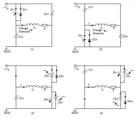
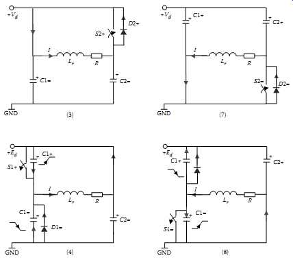
FIG. 16 The soft-switching process of a voltage-fed converter.
Employing parallel soft-switching capacitors helps to eliminate or contain the turnoff losses. When the dead-time considerations are added, the necessary gate control signals and resultant voltage and current waveforms are illustrated in FIG. 15. The switching process of the active switches under steady-state conditions can be divided into eight states, and their corresponding equivalent circuits are shown in FIG. 16, where the inductor Lr represents the net residue inductance of the tuned track. These eight states are described in detail below:
1. Assume the first state starts at t0 when switch S1+ turns on. As both S1+ and S2- are on (S1- and S2+ are off), the output voltage is positive and equals to Vd. Owing to the above-resonance tuning (lagging power factor), the track current lags the fundamental of the driving voltage and changes its direction after a certain time.
In the beginning, the current flows through the antiparallel body diodes of S1+ and S2-, and then switches S1+ and S2- themselves begin to conduct after the current changes direction.
2. State 2: t1-t2. S2- turns off at t1 before S2+ turns on at t2, leaving the required dead time. Because of the existence of the capacitor C2-, the voltage across S2- cannot increase suddenly. During the short switch-off time of S2-, the voltage remains almost zero therefore zero-voltage turn-off is approximately achieved. Later, C2+ is discharged and C2- is charged gradually resulting in a ramped voltage change across the track. If the voltage across C2+ is completely discharged corresponding to fully charging C2- from zero to Vd, then D2+ begins to conduct to keep the continuity of the track current. The track voltage drops to near zero (about -1 V).
3. State 3: t2-t3. S2+ is switched on at t2. If D2+ conducts, it clamps the voltage across S2+ to almost zero so that zero-voltage switch-on of S2+ is achieved. In fact, S2+ is also switched "on" at zero current because it does not conduct before the current changes direction. Therefore an ideal "soft" turn-on condition is obtained.
4. State 4: t3-t4. S1+ switches off at t3. Similar to state 2, zero-voltage switch-off of S1+ is achieved because the voltage across C1+ increases slowly. When C1- is fully discharged, D1+ begins to conduct.
5. State 5: t4-t5. S1- is switched on at t4. If D1- conducts, then zero-voltage switch-on of S1- is achieved. As both S1- and S2+ are on, the output track voltage is -Vd. In this period, similar to state 1, the current changes direction. In the beginning, the body diodes conducts, then the switches S1- and S2+ begin to conduct after the current changes direction
6. State 6: t5-t6. S2+ is switched off at t5. The process is very similar to states 2 and 4; ZVS during the "off" state is achieved for S2+. When C2- is fully discharged, D2- begins to conduct, offering a zero-voltage turn-on condition for S2-.
7. State 7: t6-t7. S2- is switched on at t6. D2- conducts and clamps the voltage across S2- almost to zero so that zero-voltage switch-on of S2+ is achieved. Similar to other turn-on situations, after S2+ is switched on, it does not begin to conduct immediately since the current has not changed direction.
8. State 8: t7-t8. S1- is switched off at t7. Zero voltage switch-off of S1+ is achieved due to the slow charge up of C1-. When C1+ is fully discharged, D1+ begins to conduct. After this, S1+ can be switched on at zero voltage and the switching cycle repeats from state 1.
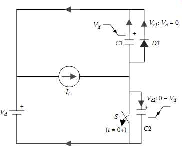
FIG. 17 Equivalent circuit of capacitor charging and discharging during dead
time.
From the above analyses it can be seen that due to the charging/discharging of the soft-switching capacitors, the PWM output voltage waveform is trapezoidal rather than square wave. Switching occurs at zero voltage or zero current instants so that the switching losses are essentially eliminated. Moreover, the stresses on the semiconductor devices are alleviated as all the transitions are "soft" at the switching instants. There are essentially no reverse-recovery problems for the diodes. Compared to direct hard-switching methods, an additional advantage of this soft-switching technique is that electromagnetic interference is reduced due to reduced dv/dt, di/dt, and improved resultant track current waveforms.
However, the above analysis also shows that this soft switching is conditional.
Specifically, the turn-on of the switches is critical. If the soft-switching capacitors are not completely charged/discharged during the dead time, the residue voltage will be shorted by the switches during turn-on, which may cause the switching devices to fail.
The essential issue here is that the track must be tuned above resonance, which ensures that the track impedance is inductive and the current has the right polarity to charge/ discharge the capacitors. Also, the inductive energy stored in the track in the residual inductance needs to be large enough to charge/discharge the capacitors fully to avoid shorting these capacitors during turn-on.
Assuming the track current is constant at IL during the dead time, the charging/ discharging process can be modeled with the simple circuit shown in FIG. 17.
Considering the initial conditions Vc1(0) = Vd and Vc2(0) = 0 when switch S is turned off at time t = 0, the voltage across the capacitor C1 during its discharging period (before the diode D starts to conduct) can be expressed as:
…where C1 = C2 = C, and Vd is the DC power supply voltage. If the dead time is given as Δt, from this equation it can be shown that the following condition should be met to guarantee safe soft-switching operation:
… when designing the soft-switching capacitors. If the capacitance is too large, the track residual inductor will not be able to fully charge/discharge it. As a result, their parallel switches at turn-on will short circuit the capacitors. However, if the capacitance is too small, the capacitor voltages will increase too fast during the turn-on time and the soft switching will be practically impossible. Therefore there is a trade-off between a desirable zero-voltage switching condition and avoiding device failure.
FIG. 18 Proposed DC-AC converter without external controllers.
On the other hand, from the track network side proper track tuning is required to achieve soft switching. A basic requirement is that the track network should be able to supply enough inductive energy to charge up the soft-switching capacitors.
In practical inductance needs to be large enough to charge/discharge the capacitors fully to avoid shorting these capacitors during turn-on.
In practical operation, the parameters of the track inductor and its tuning capacitors may cause some variation in the residue inductance Lr. In addition, load changes also affect the track current value IL during the dead-time period. Therefore it is a nontrivial task to maintain the soft-switching performance without compromising system security. Dynamic parameter tuning may be a solution, but a more economical approach is to allow the frequency to vary during operation.
A Self-Sustained Current-Fed Resonant Converter
Converter Structure:
Various current-fed resonant converters with ZVS controllers have been developed and successfully put into practical IPT applications [7,8]. Although external controllers are used in these converters, a careful look into these systems reveals that there is in fact no direct control over the output voltage, current, or frequency. The required track current is actually indirectly obtained via ZVS control. The track current output may have some slight variations in magnitude and frequency, but these variations are so small under normal working conditions that the converters are acceptable for IPT applications.
In fact, the main function of the track power supply of an IPT system is to provide high-frequency AC power in a form of magnetic field; thus a constant track current while desirable is not an absolute requirement. The secondary pickups normally have their own control units, which can regulate power flow as required by the load.
Based on the above concept and the particular application, a novel converter that can start up and keep sustained ZVS operation without any additional controllers is proposed.
This converter is essentially an autonomous system that gives the same performance as the G1 power supply. As shown in FIG. 18, it comprises a DC inductor Ld, a phase-splitting transformer Lsp, two switching devices SA and SB, and a parallel resonant tank. The DC inductor forms an approximate current source from the DC voltage supply Vd provided the inductance is large. The phase-splitting transformer replaces the two top switches of a single-phase full inverting network and essentially divides the DC current into two legs of the inverter network. Compared to the full-bridge topology, a push-pull configuration simplifies the gate drive design (as no isolation is required) and doubles the output resultant resonant voltage. The parallel resonant tank consists of an inductor L and a capacitor C, with an equivalent load resistor R that is series connected.
In other applications such as DC-DC converters [9,10], the load can also be connected in parallel as illustrated in the lower dotted block of FIG. 18.
For this current-fed converter (FIG. 18), ZVS not only minimizes switching losses and EMI but also is crucial for safe operation of the circuit. If ZVS fails, then the resonant capacitor C will be shorted by the active switches and their body diodes, which may cause the switching devices to fail. In some topologies, additional diodes are placed in series with the active switches SA and SB to prevent the shorting and allow for non-ZVS operation, but these diodes cause voltage drops and power losses so they are not commonly used.
Unlike conventional converters with two function blocks comprising the main circuit and the controller, FIG. 18 shows a novel approach of driving the switching devices without any additional controllers. Both the power and signals needed for the gate drive are obtained directly from the voltages across the main switching devices. The circuit is so simple that only a resistor and a zener diode are used for each switch. The voltage rating of the zener diodes DA and DB are chosen according to the switching requirements of the devices, for example, 4.7-5.6 V for most low-voltage threshold MOSFETs and 12-15 V for IGBTs. The current limiting resistors RA and RB are designed according to the resonant voltage level and the current rating of the zener diodes.
Self-Sustained Operation Analysis:
In principle, autonomous operation of the converter shown in FIG. 18 is based on the oscillatory property of the proposed topology. The critical conditions of the series loaded parallel-resonant tank have been investigated, and it has been found that the minimum bounds on Q to ensure start-up and steady-state ZVS operation of such series-load converters are 2.54 and 1.86 respectively [6, 8]. Theoretically there is no limit on Q for a standard parallel-loaded tank (see FIG. 18) as no DC offset voltage exists across the load resistor.
An advantageous feature of the proposed resonant converter is that it can start up automatically. At turn-on, switches SA and SB are initially "off." Once the DC source is switched on, a DC voltage will be exerted across the switches. In consequence both the switches are turned on and the current in the DC inductor increases, resulting in some energy storage in the DC inductor, which has been proven beneficial for boosting the circuit oscillation [6]. Due to the existence of parameter differences and external disturbances, the voltages across the active switches cannot be exactly the same in a practical circuit. The lower voltage, say VA, will provide a lower gate drive voltage VGB in the other leg. Consequently, SB will turn off, resulting in a higher voltage drop VB, which will further increase the gate drive voltage VGA and decrease the voltage VA. This positive feedback will quickly (typically within several ms) lead to complete resonant operation with ZVS.
FIG. 19 shows typical steady-state voltage and current waveforms of the converter obtained from a PSpice simulation. It can be seen that the gate drive signal of one switch is in fact the capped voltage across the other switch. Switch transitions occur approximately at the zero voltage points with a maximum error of a zener diode voltage drop (4.7 V). The resultant resonant voltage waveform is very good as shown.
===
Resonant voltage
Switch voltages
Gate drives
Switch current
3.8ms 3.9ms 4.0ms Time 3.6ms 3.7ms
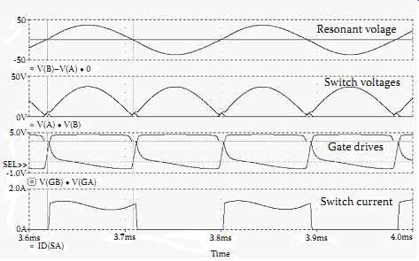
FIG. 19 Typical simulated waveforms of the proposed converter.
===
If the resonant voltage is below the zener diode voltage level, the gate drive voltage becomes very small and both switches tend to switch off. This should be strictly prohibited for current-fed resonant converters, because the DC current has to continue to avoid the occurrence of dangerously high voltages. Fortunately, the proposed converter can protect the overvoltage automatically. From FIG. 19 it can be seen that if the voltage VB is lower than the zener diode voltage 4.7 V, the gate voltage VGA starts to drop. When VGA reaches the threshold voltage of about 3 V, switch SA starts to turn off, causing a rapid voltage rise that turns the other switch SB on very quickly. As a result, the DC current follow continues and the occurrence of a high overvoltage is avoided. Since in practice, switches turn on faster than they turn off, and no external control loop delay exists in this converter, it is impossible for the dynamic voltage to become too high, although small glitches occur in the voltage waveforms of VA and VB during the switch transitions as shown in FIG. 19.
The gate drive waveforms shown in FIG. 19 have a reasonably good rising edge because they are directly driven by the large resonant voltages across the main switches, which quickly rise above 5 V. However, the falling edge of the gate drive lasts longer due to the large resistance in the discharge path of the gate input capacitor and the Miller effect. Theoretically a higher resonant voltage and higher frequency will make both the rising and falling edge of the gate drive signal sharper if only a simple resistor and zener diode circuit is considered, but practically the need for larger limiting resistances RA and RB and stronger Miller effect at high voltages may prevent the devices from turning off.
At low voltages, all these effects are small so that circuit oscillation can be sustained and the circuit functions well. An advantageous factor of this circuit is that the turn-on process is faster so that the current is quickly diverted away, which helps the switch to turn off. FIG. 19 shows that the tail current of the switch (ID) lasts a very short time. Also, the Miller effect is small during turn-on, but it helps to reduce the gate drive voltage during the fall period of the resonant voltage in the second half of the waveform. The gate voltage can become negative (as shown in FIG. 19) because the zener diode becomes forward biased as the Miller capacitor discharges. This ensures that the switch is turned off completely before it is turned on again in the next switching cycle.
It should be noted that although some distortions exist over the switch voltages during circuit transitions, they hardly appear in the final resonant voltage waveforms as shown in FIG. 19. In consequence, the resultant resonant current in the track loop contains very low harmonic components and produces minimal EMI radiation.
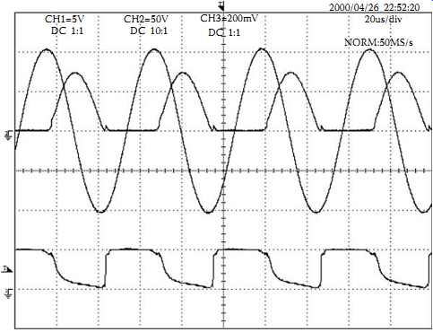
FIG. 20 Experimental result of the proposed converter (Ch1: Gate drive voltage:
5 V/div, Ch2: Switch voltage: 50 V/div, Ch3: track current: 2 A/div).
Experimental Results and Discussion:
A prototype converter of the form of FIG. 18 with parameters of L = 200 μH, C = 0.47 μF, Ld = 0.2 mH, Lsp = 2 mH, and RA = RB = 1 kΩ, and a zener diode of 5.1 V/1 W, was built and tested in the laboratory using 100 V/8 A/0.4 Ω MOSFETS. The converter can start up automatically by just turning on the main switch of a regulated DC power supply without employing any start-up equipment. FIG. 20 shows the measured waveforms of the switching voltage over switch SA (a half wave), the track current (a full wave), and the gate drive signal VGA. The DC input voltage Vd is 24 V, and the equivalent load resistance R on the track is 1 Ω. It can be seen from this result that switching occurs approximately at the zero-voltage crossing points as expected, and the sinusoidal waveform of the resonant current is perfectly acceptable.
The above test was based on a series-connected load (see FIG. 18). A parallel connected load gave very similar results. In both the cases, the converter could start up automatically and keep self-sustained ZVS. The resonant voltage and current vary proportionally to the DC input voltage, and it has been observed that the gate drive waveforms improve with increasing the DC input voltage. Nevertheless, the increase is limited by the power ratings of the resistors and zener diodes of the gate drive circuit so that operating at high voltages is impractical, as will be discussed later. Moreover, the operating frequency of the converter can be adjusted by simply varying the capacitor or inductor of the resonant circuit, and this can even be done during operation. Under such variations, the converter automatically adapts to the new operating conditions with dynamic ZVS operation. There is no danger of damaging the switching devices owing to the inherent overvoltage protection property of the converter discussed earlier.
Because of the elimination of any external controllers, the system delay and the total component count is greatly reduced. This helps to increase the maximum possible operating frequency and power density, as well as improve the power efficiency and reliability at reduced cost. However, as with the G1 and variable frequency power supplies based on free oscillation and energy injection control, the operational frequency of this converter is dependent on the load so that frequency stability problems can occur. As such the design of a complete IPT system using such converters requires care to achieve the required power transfer capacity.
Apart from the above example converter based on the current-fed parallel-resonant G1 supply, there are other options to achieving a self-sustained switch-mode operation that are worth further exploration in the future. One potential application of this type of converter is in the development of higher-frequency converters (say 1-10 MHz) aiming to significantly increase the power density. It is known that the design of gate drives becomes difficult at such high frequencies for normal low-voltage drive circuits.
Surprisingly, it can be easier for the self-sustained converters to achieve desirable gate drive waveforms because the required signals and power are integrated and internally supplied from the main circuit where high-frequency voltages or currents are available.
To overcome the shortcomings of this type of converter regarding the lack of control flexibility, other control mechanisms such as varying circuit parameters (rather than via gate drive control) may be used to regulate the final output as required.
Gate Drive Improvement:
The self-sustained converter is shown to be both simple and effective. However, the autonomous simple gate drive circuit does not give ideal gate drive waveforms. Also, at high voltages the current limiting "dropper" resistors and zener diodes of the gate drive circuit become lossy, which will reduce the overall power efficiency of the power converter.
A possible solution is to have a voltage-controlled nonlinear resistor as shown in FIG. 21(a). If the resistance of this variable resistor decreases as the voltage across it decreases, then the problems discussed above can be solved automatically. In high-voltage periods, the resistance is high so that the power losses are low. Conversely, during the low-voltage transition periods, the resistance is low so that both the rising edge and falling edge of the gate drive signal can be improved. Unfortunately, no suitable resistor with such a nonlinear property has been found in the commercial market. Normal thermally variable resistors are far too slow for this application.
Alternatively, adding additional components, such as a speed-up capacitor in parallel with the current-limiting resistor as shown in FIG. 21(b), can provide a phase advance and reduce the transition delay. However, the dilemma is that a small capacitance has little effect, but a large capacitance makes the gate drive voltage drop too early before the actual zero-voltage crossing due to the fact that the resonant voltage starts to drop in the second half of the "off" period. As noted, turning the devices off too early interrupts the DC current flow and causes high overvoltages, which may damage the switching devices. As a result, more sophisticated charging and discharging circuits are needed to achieve desirable gate drive waveforms for high-voltage applications.
To further improve the gate drive waveforms and power losses, PLL (phase-locked loop) and direct ZVD (zero-voltage detection) techniques were investigated to build more efficient IPT power supplies. In these two cases, although gate controllers are used essentially they only help to follow zero-voltage crossings of the resonant voltage, so the current is still autonomous.
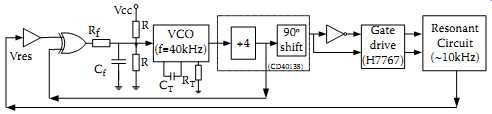
FIG. 22 PLL gate drive technique.
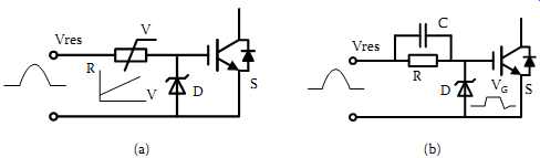
FIG. 21 Passive gate drive circuits for the self-sustained resonant converter:
(a) using a voltage-controlled variable resistor; (b) using a speed-up capacitor.
===
Vdc R D C Vres Zero voltage detection Start-up timing Logic
(Self supplied DC power to gate drive circuits)
Gate drive (H7667) Resonant Circuit (~10kHz)
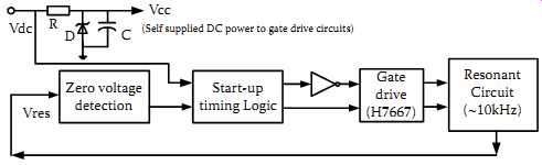
FIG. 23 Direct ZVD gate drive technique.
===
FIG. 22 is a block diagram showing how the PLL technique can be used to control a resonant circuit. In this diagram the VCO (voltage-controlled oscillator) unit is set at a predetermined frequency by a resistor RT and a capacitor CT, say 40 kHz, when its input voltage is set at half the DC supply voltage Vcc by two equal resistors R. The output from the VCO is divided by 4 to obtain the system nominal frequency (e.g., 10 kHz here) and a phase shift of 90° using a normal D flip-flop circuit. Then the output signal is divided into two complementary signals and sent to an IGBT gate drive circuit (such as ICL 7667) to drive the two main switches of the resonant circuit. From the ZVS frequency analysis of the current-fed resonant converter undertaken, it has been shown that the switching frequency has to be varied to achieve ZVS operation. For this reason, the resonant voltage (v_res) of the main circuit is detected and fed back to change the actual operating frequency, which can be slightly higher or lower than the nominal frequency. The resonant voltage may be measured directly across the two main switching devices; however, the voltage measured will be very high so a voltage divider with a very large turn-down ratio has to be used, and this is not desirable to cater to a wide range of operating voltages.
Alternatively, a one-turn coil added to the phase-splitting transformer of the converter (see FIG. 18) can be employed as a very simple and reliable voltage sensor. The measured resonant voltage is converted to a square waveform using a high-gain amplifier and is then compared with the output of the VCO (after the frequency divider) using an XOR logic circuit. These two signals should be equal in frequency but have a 90º phase shift as required for the XOR detection circuit. After an RC low-pass filter, the output pulses from the XOR will control the input voltage of the VCO, thus varying the actual gate driving frequency to the point where a stable ZVS frequency is obtained.
Unlike the PLL gate drive, which is based on frequency shift control, FIG. 23 shows the block diagram of a direct ZVD technique. The advantage of this technique over PLL is that after the resonant voltage is measured, the zero crossings of the resonant voltage are detected instantly using a zero-voltage detection circuit, and the output is used to control the gate drive directly. However, the current-fed resonant converter has a start-up problem because the resonant voltage does not go to zero naturally in the beginning. A complete new technique is used to overcome this problem. On starting, both switches are turned on at the same time so that the current in the DC inductor increases rapidly. When enough energy is stored in the inductor compared to the energy in the resonant circuit in normal operation, one switch is turned off and the circuit then completes a first half-cycle followed by normal operation with direct ZVS control. To achieve this desirable condition, start-up timing logic is added as shown in FIG. 23. Also, to avoid an additional DC power supply for the gate control circuitry and form a completely self-sustained converter, a simple zener diode configuration is used although the initial power buildup process has to be considered to make the circuit work properly. If the ramp-up delay of a practical input DC supply is taken into account, an overshoot-free soft start-up can be achieved. Consequently, the system can start up simply by turning on the main switch of the input power supply without employing any additional equipment.
FIG. 24 shows the measured steady-state resonant voltage (across one of the main switches) and the gate signal waveforms of a practical 80 A/10 kHz current-fed parallel resonant IPT power supply using the direct ZVD technique. The DC input voltage is 240 V and the DC current can be up to 60 A, corresponding to a maximum load of about 15 kW. The main circuit of the converter is the same as the self-sustained converter (essentially the G1 power supply) shown in FIG. 18. The track inductance is 125 μH, and its parallel tuning capacitance is about 2μF. It can be seen that ZVS operation is achieved and both the rising and falling edges of the gate drive waveform are significantly improved owing to the adoption of the specially designed MOS gate drive circuit (ICL 7667).
A PLL circuit was also built to control a power converter with the same specifications as that of the direct ZVD. Because the same gate drive chip was used, very similar gate signal waveforms were obtained. To avoid repetition, FIG. 24 shows the resonant voltage and the resultant track current of this IPT power supply. In fact, it has been observed that the track current waveforms of the two supplies are basically the same because they achieve very similar steady-state ZVS performance. However, a close look at the resonant voltage waveforms shows that the switching of the ZVD scheme is slightly slower due to the circuit delay (which is mainly caused by the practical comparator used). In comparison, the average ZVS error of the PLL circuit can be smaller under ideal steady-state conditions because it has an integral control loop and can add in some phase advance to the gate drive signals. However, this is true only when the feedback loop of the PLL is tuned accurately. Practical circuit parameter and voltage variations can introduce errors in the PLL circuit, and as a result the actual difference between the steady-state ZVS errors of the two IPT power supplies is barely perceptible.
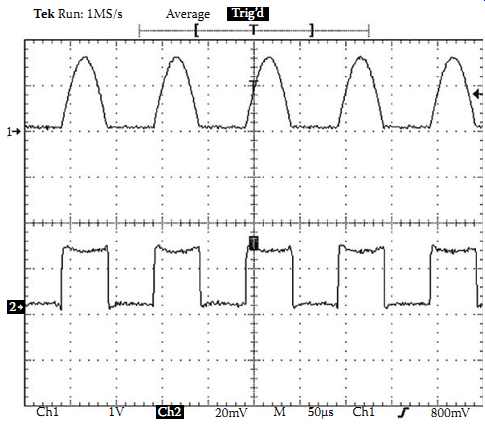
FIG. 24 Steady-state waveforms of an IPT power supply using direct ZVD (Ch1:
Resonant voltage across the switch: 500 V/div, Ch2: Gate drive signal: 10
V/div).
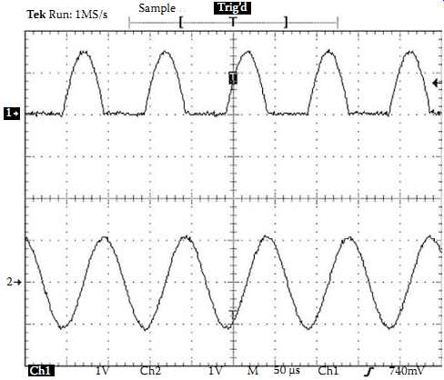
FIG. 25 Steady-state waveforms of an IPT power supply using PLL (Ch1: Resonant
voltage across the switch: 500 V/div, Ch2: Track current: 100 A/div).
Apart from being simple and cost-effective, the most outstanding advantage of the direct ZVD circuit over the PLL is its dynamic performance. The PLL circuit has a predetermined frequency, and its internal "integral" process causes relatively slow frequency response so that dynamic ZVS is impossible. As a result, additional blocking diodes have to be put in series with the main switches for safe operation, and special care has to be taken in designing the PLL circuit to ensure the frequency can be captured by the PLL during start-up and load transients. Conversely, the ZVD circuit simply follows the zero voltage crossings with limited predictable errors during the whole process so that the series-blocking diodes are optional. Although frequency stability problems may occur under some extreme conditions as discussed previously, during normal working conditions the circuit oscillation continues and the direct ZVD operation is very reliable. The actual operating frequency can be varied simply by changing the resonant inductor or the parallel-tuning capacitor without any modification of the gate drive circuit. The basic concept employed here is essentially the same as the simple self-sustained converter proposed earlier, but the gate-drive performance is significantly improved.
Using the method discussed above, an 80 A/10 kHz IPT power supply based on direct ZVD has been built and overshoot-free dynamic ZVS start-up and steady-state performance has been achieved. FIG. 25 shows a measured result of the resonant voltage across one of the two main switches and the gate drive signal of the other switch. It can be seen that the voltage across the switch, which is equal to the DC input voltage, ramps up gradually in the beginning when both the switches are off. After a very short DC current buildup period (where both the switches are on, shown with the first short pulse of the gate drive signal in FIG. 26) before the DC voltage reaches its maximum value, the circuit goes into ZVS operation very quickly and smoothly without any overshoots. As a result, the stresses and losses of the switching devices are minimized. This feature is particularly useful for applications where frequent "on" and "off" control of the converter is required. An IPT pulse battery-charging system controlled from the primary side is a good example of such an application.
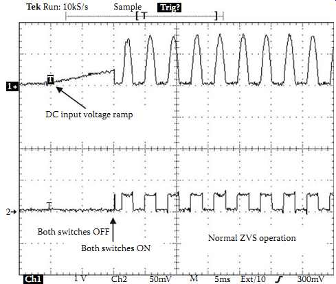
FIG. 26 Start-up waveforms of a practical IPT power supply using direct ZVD
(Ch1: Resonant switch voltage: 500 V/div)
References
1. Luo, Fang Lin, and Hong Ye. 2004. Advanced DC/DC converters. Boca Raton, FL: CRC Press.
2. Mohan, N., T. M. Undeland, and W. P. Robbins. 1995. Power electronics-converters, applications, and design. New York: Wiley.
3. Ang, Simon, and Alejandro Livia. 2005. Power-switching converters, 2nd ed. Boca Raton, FL: CRC Press.
4. Kularatna, Nihal. 2008. Electronics circuit design-from concept to implementation. Boca Raton, FL: CRC Press.
5. NXP Philips Semiconductors. 2007. TEA1610P, TEA1610T zero-voltage-switching resonant converter controller. Product Data Sheet, rev. 03, March.
6. Hu, Aiguo Patrick. 2009. Wireless/contactless power supply-inductively coupled resonant converter solutions. Saarbrücken, Germany: VDM Verlag.
7. Green, A. W., and J. T. Boys. 1994. 10 kHz inductively coupled power transfer- concept and control. IEE Power Electronics and Variable Speed Drives Conference, PEVD, Pub. 399, 694-99.
8. Boys, J. T., A. Hu, and G. Covic. 2000. Critical Q analysis of a current-fed resonant converter for ICPT applications. IEE Electronics Letters 36 (17, ISSN 0013-5194, August): 1440-42.
9. Luo, Fang Lin, and Hong Ye. 2006. Synchronous and resonant DC/DC conversion technology, energy factor, and mathematical modeling.