AMAZON multi-meters discounts AMAZON oscilloscope discounts
... (<< cont. from part 1)
Power MOSFETs
Introduction
Compared to BJTs, which are current-controlled devices, field-effect transistors (FETs) are voltage-controlled devices. There are two basic FETs: the junction FET (JFET) and the metal-oxide semiconductor FET (MOSFET). Both have played important roles in modern electronics. The JFET has found wide application in such cases as high-impedance transducers (scope probes, smoke detectors, etc.) and the MOSFET in an ever-expanding role in integrated circuits, where CMOS (complementary MOS) is perhaps the most well known.
Power MOSFETs differ from bipolar transistors in operating principles, specifications, and performance. In fact, the performance characteristics of MOSFETs are generally superior to those of bipolar transistors: significantly faster switching time, simpler drive circuitry, the absence of a second breakdown failure mechanism, the ability to be paralleled, and stable gain and response time over a wide temperature range. The MOSFET was developed out of the need for a power device that could work beyond the 20 kHz frequency spectrum, anywhere from 100 kHz to above 1 MHz, without experiencing the limitations of the bipolar power transistor.
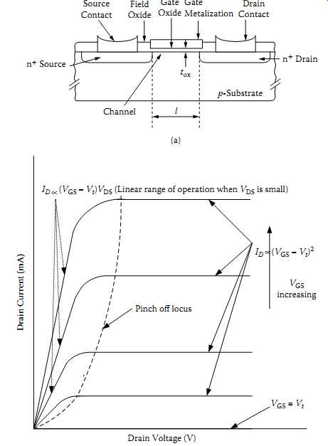
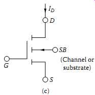
FIG. 26 Structure of a MOSFET, characteristics, and symbol: (a) basic concept;
(b) characteristics; (c) symbol for n-channel device.
General Characteristics
Bipolar transistors are described as minority-carrier devices in which injected minority carriers recombine with majority carriers. A drawback of recombination is that it limits the device's operating speed. Current-driven base-emitter input of a bipolar transistor presents a low-impedance load to its driving circuit. In most power circuits, this low impedance input requires somewhat complex drive circuitry.
By contrast, a power MOSFET is a voltage-driven device whose gate terminal is electrically isolated from its silicon body by a thin layer of silicon dioxide (SiO2) as shown in the simplified schematic of a MOSFET shown in FIG. 26(a). The n-channel device formed on a p-substrate carries two n+ regions for the drain and the source areas between which a channel of length l is formed. As a majority-carrier semiconductor, the MOSFET operates at much higher speed than its bipolar counterpart because there is no charge-storage mechanism. A positive voltage applied to the gate of an n-type MOSFET creates an electric field in the channel region just beneath the gate oxide region with a thickness of tox; that is, the electric charge on the gate causes the p-region beneath the gate to convert to an n-type region, as shown in FIG. 26(a).
This conversion, called the surface-inversion phenomenon, allows current to flow between the drain and source through an n-type material. In effect, the MOSFET ceases to be an NPN device when in this state. The region between the drain and source can be represented as a resistor, although it does not behave linearly, as a conventional resistor would. Because of this surface-inversion phenomenon, the operation of a MOSFET is entirely different from that of a bipolar transistor.
There are different commercial variations of power MOSFETS, usually referred to as planar and trench designs. FIG. 27(a) indicates the details of planar MOSFET, and Figures .27(b) and 27(c) indicate trench MOSFET versions known as current-crowding V-groove Trench MOSFET and the truncated V-groove MOSFET.
By virtue of its electrically isolated gate, a MOSFET is described as a high-input impedance, voltage-controlled device, compared to a bipolar transistor. As a majority carrier semiconductor, a MOSFET stores no charge and so can switch faster than a bipolar device. Majority-carrier semiconductors also tend to slow down as temperature increases. This effect brought about by another phenomenon called carrier mobility makes a MOSFET more resistive at elevated temperatures, and much more immune to the thermal runaway problem experienced by bipolar devices. Mobility is a term that defines the average velocity of a carrier in terms of the electrical field imposed on it.
A useful by-product of the commercially produced MOSFETs is the internal parasitic diode formed between source and drain, as shown in right-hand side of FIG. 27(b). (There is no equivalent for this diode in a bipolar transistor other than in a bipolar Darlington transistor.) Its characteristics make it useful as a clamp diode in inductive-load switching.
Different manufacturers use different techniques for constructing a power FET, and names like VMOS, TMOS, Cool MOS, etc., have become trademarks of specific companies.
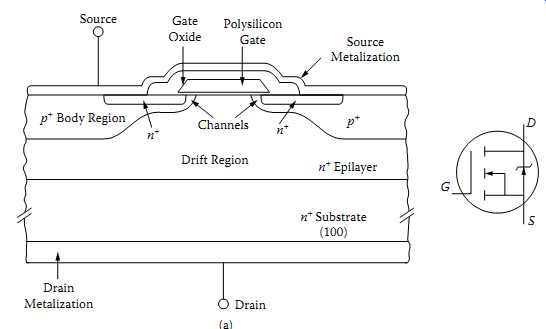
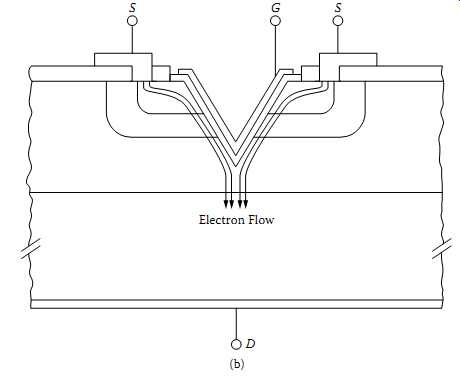
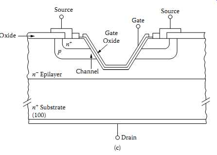
FIG. 27 Different commercial implementations of power MOSFET: (a) planar
MOSFET; (b) current crowding in V-Groove Trench MOSFET; (c) truncated V-groove
MOSFET
Source Source Metalization
Gate Oxide
p+ Body Region
n+ n+
n+ Epilayer
n+ Substrate (100)
p+ Channels Drift Region Drain
Drain Metalization Polysilicon Gate
=======
MOSFET Structures and On Resistance
Most power MOSFETs are manufactured using various proprietary processes by various manufacturers on a single silicon chip structured with a large number of closely packed identical cells. For example, Intersil (formerly Harris Semiconductor) power MOSFETS are manufactured using a vertical double-diffused process, called VDMOS or simply DMOS. In these cases, a 120 mil2 chip contains about 5000 cells and a 240 mil2 chip has more than 25,000 cells.
One of the aims of multiple-cells construction is to minimize the MOSFET parameter RDS(ON) when the device is in the on-state. When RDS(ON) is minimized, the device provides superior power-switching performance because the voltage drop from drain to source is also minimized for a given value of drain-source current. Reference [6] provides more details.
FIG. 28(a) indicates different components of resistances (contributing to RDS(ON)) and stray capacitances contributing to delays in operation of the devices. In addition a power MOSFET comes with a few parasitic devices such as diodes, BJT, and a JFET in general. The on resistance of a power MOSFET is made up of several components as shown in FIG. 28(b) where…
…where Rsource is the source diffusion resistance, RCh is the channel resistance, RA is the accumulation resistance, RJ is the JFET component, RD is the drift region resistance, and RSub is the substrate resistance.
Rwcml is the sum of many components contributed by the bond wire, contact resistance between the source and drain, metallization, the silicon and any lead frame contributions.
Following the relationship in [42] for the specific on resistance, Ron, sp, neglecting secondary effects, indicates that the higher-voltage devices usually have a higher on resistance …
…where R_on, sp is the RDS (on) per unit area, and μ is the mobility of electrons (for n-channel devices), and BVDSS is the maximum drain-source voltage. Wafers with substrate resistivity of up to 20 mΩ ⋅cm are used for high-voltage devices and less than 50 mΩ.cm are used for low-voltage devices in general. Rwcml component's contribution in high-voltage devices is negligible in general. At high voltages the RDS(on) is dominated by the contribution from the epi-layer components [41].
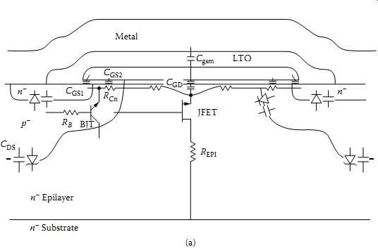
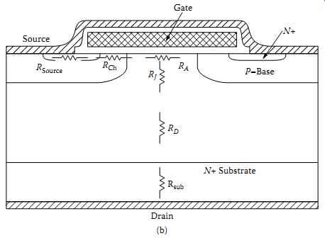
FIG. 28 Power MOSFET details related to fabrication: (a) internal resistances,
stray capacitances, and parasitic devices; (b) components contributing to
RDS(on).
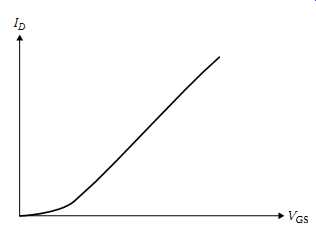
FIG. 29(a) Transfer characteristics of a power MOSFET.
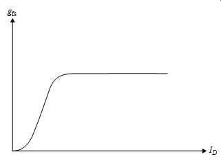
FIG. 29(b) Relationship of transconductance (gfs) to ID of a power MOSFET.
I-V Characteristics
FIG. 26(b) shows the drain-to-source operating characteristics of the power MOSFET.
Although the curve is similar to the case of the bipolar power transistor ( FIG. 17), there are some fundamental differences.
The MOSFET output characteristic curves reveal two distinct operating regions, namely a "constant resistance" and a "constant current." Thus as the drain-to-source voltage is increased, the drain current increases proportionally, until a certain drain-to source voltage called pinch-off is reached. After pinch-off, an increase in drain-to-source voltage produces a constant drain current.
When the power MOSFET is used as a switch, the voltage drop between the drain and source terminals is proportional to the drain current; that is, the power MOSFET is working in the constant resistance region, and therefore it behaves essentially as a resistive element. Consequently, the on-resistance RDS(ON) of the power MOSFET is an important figure of merit because it determines the power loss for a given drain current, just as VCE,sat is of importance for the bipolar power transistor.
By examining FIG. 29(a), we note that the drain current does not increase appreciably when a relatively low gate-to-source voltage is applied; in fact, drain current starts to flow after a threshold gate voltage has been applied, in practice somewhere between 2 and 4 V. Beyond the threshold voltage, the relationship between drain current and gate voltage is approximately linear. Thus the transconductance gfs, which is defined as the rate of change of drain current to gate voltage, is practically constant at higher values of drain current. FIG. 29(a) illustrates the transfer characteristics of ID versus VGS, while FIG. 29(b) shows the relationship of transconductance gfs to drain current.
It’s now apparent that a rise in transconductance results in a proportional rise in the transistor gain, i.e., larger drain current flow, but unfortunately this condition swells the MOSFET input capacitance. Therefore carefully designed gate drivers must be used to deliver the current required to charge the input capacitance in order to enhance the switching speed of the MOSFET.
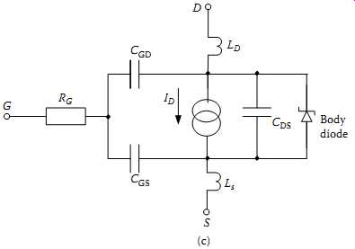
FIG. 29(c) Equivalent circuit of a MOSFET.
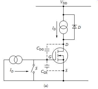
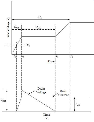
FIG. 30 MOSFET switching behavior: (a) test circuit; (b) waveforms.
Gate Drive Considerations
The MOSFET is a voltage-controlled device; that is, a voltage of specified limits must be applied between gate and source in order to produce a current flow in the drain.
Since the gate terminal of the MOSFET is electrically isolated from the source by a silicon oxide layer, only a small leakage current flows from the applied voltage source into the gate. Thus the MOSFET has an extremely high gain and high impedance.
Threshold voltage, Vt, is defined as the minimum gate electrode bias required to strongly invert the surface under the poly-silicon gate region and form a conducting channel between the source and the drain regions. Vt is usually measured at a drain current of 250 μA in general. Common voltages are 2-4 V for high-voltage devices and 1-2 V for lower-voltage logic-compatible devices. With these devices finding increasing use in portable systems with battery power at a premium, the trend is toward lower values of RDS(on) and Vt.
The switching performance of a device is determined by the time required to establish voltage changes across capacitances and current changes in inductances. In the equivalent circuit shown in FIG. 29(c), RG is the distributed resistances of the gate and is approximately inversely proportional to the active area. Ls and LD are source and drain lead inductances that are around few 10s of nH. Typical values of input (Ciss), output (Coss), and reverse transfer (Crss) capacitances given in data sheets are related to capacitances shown in FIG. 29(c). The following relationships are used to estimate the typical values.
CGD, gate-to-drain capacitance, is a nonlinear function and is the most important parameter because it provides a feedback loop between the output and the input of the circuit. This parameter is also called the Miller capacitance because it causes the total dynamic input capacitance to become greater than the sum of the static capacitances.
In designing gate drive circuits, more useful set of parameters are gate charges than the gate capacitances. FIG. 30(b) depicts typical charging process and the waveforms.
When the gate is connected to a voltage source, gate source voltage starts to increase until it reaches Vt at which point the drain current starts to flow. With the charging of CGS gate voltage continues to rise (during the period t1-t2), and the drain voltage rises proportionately.
At time t2, CGS is completely charged, and the drain current reaches the predetermined value (based on external circuit) and stays constant. Referring to the test circuit in FIG. 30(a) when the CGS is fully charged at t2, VGS becomes constant and the drive current starts to charge the Miller capacitance CDG. This continues until time t3. From t2 to t3 with the drain voltage falling linearly, the gate drive is charging the CDG. Once both capacitors are fully charged, gate voltage increases until it reaches the maximum gate drive voltage. Good circuit design practice dictates the use of a higher gate voltage than the bare minimum required for switching, and therefore the gate charged used in calculations should be the charge QG corresponding to t4. This maximum-charge approach simplifies the case of estimating any current source values (such as gate driver capabilities) where basic capacitor charge calculations can be used to estimate the charging times.
In order to turn a MOSFET on, a gate-to-source voltage pulse is needed to deliver sufficient current to charge the input capacitor in the desired time. The MOSFET input capacitance Ciss is the sum of the capacitors formed by the metal-oxide gate structure, from gate to drain (CGD) and gate to source (CGS). Thus the driving voltage source impedance Rg must be very low in order to achieve high transistor speeds. A way of estimating the approximate driving generator impedance, plus the required driving current, is given in the following equations:
... where Rg = generator impedance; Ciss = MOSFET input capacitance, pF; and dv/dt = generator voltage rate of change, V/ns.
FIG. 31(a) illustrates the relationship of drain current, ID, versus VDS when there is zero VGS applied to gate, which is the blocking characteristic of the power MOSFET.
Leakage drain current (IDSS) continues to flow until the device VDS reaches the breakdown voltage, BVDSS, at which point the body diode breaks down. BVDSS is usually measured at 250 μA drain current.
Temperature Characteristics
The high operating temperatures of bipolar transistors are a frequent cause of failure.
The high temperatures are caused by hot spotting, the tendency of current in a bipolar device to concentrate in areas around the emitter. Unchecked, this hot spotting results in the mechanism of thermal runaway, and eventual destruction of the device.
MOSFETs don’t suffer this disadvantage because their current flow is in the form of majority carriers. The mobility of majority carriers in silicon decreases with increasing temperature.
This inverse relationship dictates that the carriers slow down as the chip gets hotter. In effect, the resistance of the silicon path is increased, which prevents the concentrations of current that lead to hot spots. In fact, if hot spots do attempt to form in a MOSFET, the local resistance increases and defocuses or spreads out the current, rerouting it to cooler portions of the chip.
Because of the character of its current flow, a MOSFET has a positive temperature coefficient of resistance, as shown by the curves of FIG. 31(b).
The positive temperature coefficient of resistance means that a MOSFET is inherently stable with temperature fluctuation, and provides its own protection against thermal runaway and second breakdown. Another benefit of this characteristic is that MOSFETs can be operated in parallel without fear that one device will rob current from the others.
If any device begins to overheat, its resistance will increase, and its current will be directed away to cooler chips.
====
ID
Leakage drain current Avalanche voltage
VDS
VGS = 0 (BVDSS )
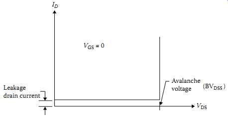
FIG. 31a Drain-to-source blocking characteristics of the MOSFET.
====
FIG. 31(b) Positive temperature coefficient of a MOSFET.
Safe Operating Area and Avalanche Rating
In the discussion of the bipolar power transistor, it was mentioned that, in order to avoid secondary breakdown, the power dissipation of the device must be kept within the operating limits specified by the forward-bias SOA curve. Thus at high collector voltages, the power dissipation of the bipolar transistor is limited by its secondary breakdown to a very small percentage of full-rated power. Even at very short switching periods, the SOA capability is still restricted, and the use of snubber networks is incorporated to relieve transistor-switching stress and avoid secondary breakdown.
In contrast, the MOSFET offers an exceptionally stable SOA, since it does not suffer from the effects of secondary breakdown during forward bias. Thus both the DC and pulsed SOA are superior to that of the bipolar transistor. In fact, with a power MOSFET it’s quite possible to switch rated current at rated voltage without the need of snubber networks. Of course, during the design of practical circuits, it’s advisable that certain derating must be observed.
FIG. 31(c) shows typical MOSFET and equivalent bipolar transistor curves superimposed in order to compare their SOA capabilities. Secondary breakdown during reverse bias is also nonexistent in the power MOSFET, since the harsh reverse-bias schemes used during bipolar transistor turn-off are not applicable to MOSFETs. Here , for the MOSFET to turn off, the only requirement is that the gate is returned to 0 V. For more details on SOA, refer to [ 43].
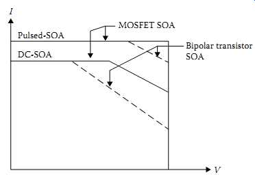
FIG. 31(c) SOA curves for power MOSFET.
Dynamic Stresses and Avalanche Failures:
MOSFET manufacturers usually specify the SOA based on static operating conditions.
However, most power electronic circuits carry inductive and capacitive components, which can cause significant transients due to:
di / dt
... and
dv / dt
…effects, and these effects require quite complex approaches to quantify accurately. Any transient has the potential to drive the drain to source of a MOSFET into avalanche. To help cope with the transients there are avalanche-resistant devices that are rated over a wide range of current, junction temperature, and time.
In a power MOSFET used in a switching circuit where inductance is switched by the device, when the device is switched off (similar to the case of a boost converter with load suddenly switching off simultaneously) inductive current could finally end up flowing through the body diode, which enters into avalanche. The maximum value of this diode current, IAS, which is given in data sheets as single-pulse drain source avalanche current, is dependent on the starting junction temperature, the time in avalanche, etc. Avalanche survivability of a power MOSFET centers on the condition that the parasitic bipolar transistor inside the device never turns on [44]. This rating, known as the unclamped inductive switching (UIS) rating, which becomes application specific, is discussed in [44-46] and is also applicable to modern high-speed power rectifiers
[46]. A test method to measure these is discussed in [46]. A practically valuable discussion with application considerations in various circuits including resonant converters is in [47]. References [48-52] are useful in estimating the reliability and modeling of power MOSFETs.
Practical Components
High-Voltage and Low-On-Resistance Devices:
Denser geometries, processing innovations, and packaging improvements in the 1990s were resulting in power MOSFETS that have ever-higher voltage ratings and current-handling capabilities. See [7-9] for more information. Bipolar transistors have always been available with very high voltage ratings, and those ratings don’t carry onerous price penalties. Achieving good high-voltage performance in power MOSFETs, however, has been problematic , for several reasons.
First, the RDS(ON) of devices of equal silicon area increases exponentially with the voltage rating. To get the on-resistance down, manufacturers would usually pack more parallel cells onto a die. But this denser packing causes problems in high-voltage performance.
Propagation delays across a chip, as well as silicon defects, can lead to unequal voltage stresses and even to localized breakdown.
Manufacturers resort to a variety of techniques to produce high-voltage (>1000 V), low-RDS(ON) power MOSFETs that offer reasonable yields. Advanced Power Technology (APT) , for example, deviates from the trend toward smaller and smaller feature sizes in its quest for low on-resistance. Instead, the company uses large dies to get RDS(ON) down.
APT manufactures power MOSFETs using dies as large as 585 × 738 mil and reaching voltage ratings as high as 1000 V. APT10026JN, a device from their product range, has a current rating of 1000 V with 690 W power rating. On-resistance of the device is 0.26 Ω.
When the devices were aimed out to low power applications such as laptop and note guide computers, cellular phones, etc., extremely low RDS(on) values from practical devices were necessary.
Specific on-resistance of double-diffused MOSFETs (DMOSFETs), more commonly known as power MOSFETs, has continually shrunk over the past two decades. In other words, the RDS(ON) per unit area has dropped. The reduced size with regard to low-voltage devices (those rated for a maximum drain-to-source voltage VDS of under 100 V) was achieved by increasing the cell density.
Most power-MOSFET suppliers now offer low-voltage FETs from processes that pack 4 million to 8 million cells/in2, in which each cell is an individual MOSFET. The drain, gate, and source terminals of all the cells are connected in parallel. Manufacturers such as International Rectifier (IOR) have developed many generations of MOSFETs based on DMOS technology. For example, the HEXFET family from IOR has gone through five generations, gradually increasing the number of cells per in2 with almost 10-fold decrease in the RDS(ON) parameter as per FIG. 32. RDS(ON) times the device die area in this figure is a long-used figure of merit (FOM) for power semiconductors. This is called specified on resistance. For details, [23] is suggested.
Because Generation 5 die are smaller than the previous generation, there is room within the same package to accommodate additional devices such as a Schottky diode.
The FETKY family from IOR [26], which uses this concept of integrating a MOSFET with a Schottky diode, is aimed at power converter applications such as synchronous regulators and the like.
In designing their DMOSFETs, Siliconix borrowed a DRAM process technique called the trench gate. They then developed a low-voltage DMOSFET process that provides 12 million cells/in2 and offers lower specific on-resistance-RDS(ON)-than present planar processes.
The first device from the process, the n-channel Si4410DY, comes in Siliconix's data guide "Little Foot" eight-pin DIP. The Si4410DY sports a maximum on-resistance of 13.5 mΩ, enhanced with 10 V of gate-to-source voltage (VGS). At a VGS of 4.5 V, RDS(ON) nearly doubles, reaching a maximum value of 20 mΩ.
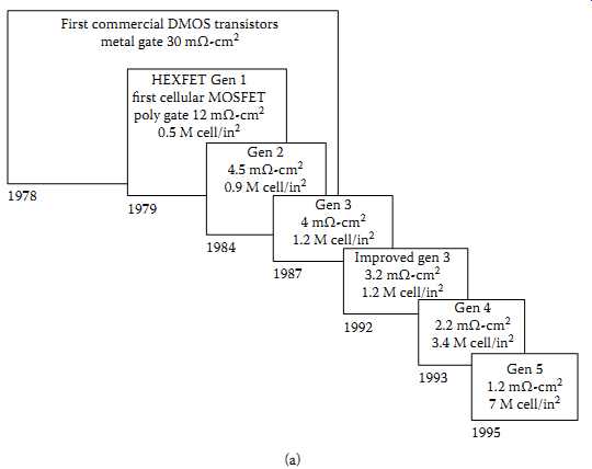
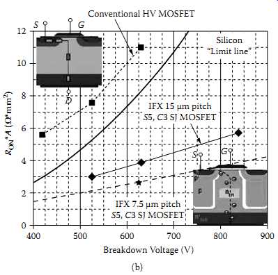
FIG. 32 The power MOSFET generations related to DMOS and the impact of super-junction
(SJ) technology: (a) DMOS generations up to 1995; (b) performance of SJ technology
with conventional high-voltage MOSFETs. (Part [a] International Rectifier.)
During the year 1997 Temic Semiconductors (formerly Siliconix) has further improved their devices to carry 32 million cells/in^2 using their TrenchFET technology.
These devices come in two basic families, namely (a) low-on-resistance devices and (b) low-threshold devices. Maximum on-resistance was reduced to 9 mΩ and 13 mΩ, compared to the case of Si 4410DY devices with corresponding values of 13.5 mΩ (for VGS of 10 V) and 20 mΩ (for VGS of 4.5 V) , for these low-on-resistance devices. In the case of the low-threshold family, these values were 10 mΩ and 14 mΩ for gate source threshold values of 4.5 V and 7.5 V, respectively. For details [27] is suggested.
By the early part of 2000, high-density DC-DC converters were mandatory to power high-power processors and processor-based portables where battery run-time optimization was a key factor in any portable design. With this power MOSFET suppliers were pressured to develop better-performing devices. Driving factors for this were the following:
• Higher efficiency with reduced switching losses
• Low RDS(on)
• Lower power dissipation
• Improved reliability
• Improved UIS
• Elimination of the need for paralleling devices for higher power
• Lower gate charge and capacitance
• Faster switching speeds
• Increased power package density
Trench-gated vertical DMOS silicon became common in the mid-2000s, providing documented and established advantages over their planar counterparts. Typical Generation 2 devices from companies such as Vishay Siliconix (an example is Si4842DY) came out around 2003 for both n-channel and p-channel devices with 32 million to 50 million cells/in^2 with on-resistances in the range of 4-5mΩ and with gate charge levels of less than 25 nC [52]. These devices were used in DC-DC converters with percentage efficiencies in the high 80s. Super-junction (SJ) MOSFETS, initially developed and introduced by Siemens, followed later by ST Microelectronics, employ a novel drain structure [54]. The first generation of these devices, known as Cool MOS, provides a better efficiency compared to common DMOS technology as the chip area increases.
For details on this technology, which appears to have beaten the silicon limit line, is discussed in [54]. FIG. 32(b) indicates this superjunction MOSFET technology performance in terms of RDS(on) * A versus the breakdown voltage.
P-Channel MOSFETs:
Historically, p-channel FETs were not considered as useful as their n-channel counterparts.
The higher resistivity of p-type silicon, resulting from its lower carrier mobility, put it at a disadvantage compared to n-type silicon.
Due to the approximately 2:1 superior mobility on n-type devices, n-channel power FETs dominate the available devices, because they need about half the area of silicon for a given current or voltage rating. However, as the technology matures, and with the demands of power-management applications, p-channel devices are starting to become available.
They make possible power CMOS designs and eliminate the need for special high-side drive circuits. When a typical n-channel FET is employed as a high-side switch running off a plus supply rail with its source driving the load, the gate must be pulled at least 10 V above the drain. A p-channel FET has no such requirement. A high-side p-channel MOSFET and a low-side n-channel MOSFET tied with common drains make a superb high-current "CMOS equivalent" switch.
Because on-resistance rises rapidly with device voltage rating, it was only recently (1994/1995) that high-voltage p-channel power MOSFETs were introduced commercially.
One such device is IXTH11P50 from IXYS Semiconductors with a voltage rating of 500 V, a current rating of 11 A, and an on-resistance of 900 mΩ.
Such high-current devices eliminate the need to parallel many lower-current FETs.
These devices make possible complementary high-voltage push-pull circuits and simplified half-bridge and H-bridge motor drives.
Recently introduced low-voltage p MOSFETs from the TrenchFET family of Temic Semiconductors [27] have typical RDS(ON) values between 14 mΩ and 25 mΩ.
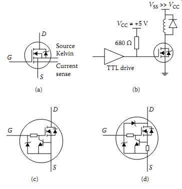
FIG. 33 Advanced Monolithic MOSFETs: (a) current-sensing MOSFET; (b) application
of a logic-level MOSFET; (c) current-limiting MOSFET; (d) voltage-clamping,
current-limiting MOSFET.
More Advanced Power MOSFETs:
With the advancement of processing capabilities, industry benefits with more advanced power MOSFETs such as:
Current-sensing MOSFETs ( FIG. 33(a)) Logic-level MOSFETs ( FIG. 33(b)) Current-limiting MOSFETs ( FIG. 33(c)) Voltage-clamping, current-limiting MOSFETs ( FIG. 33(d))
The technique of current mirroring for source current-sensing purposes involves connecting a small fraction of the cells in a power MOSFET to a separate sense terminal.
The current in this terminal (see FIG. 33(a)) is a fixed fraction of the source current feeding the load. Current sense lead provides an accurate fraction of the drain current that can be used as a feedback signal for control and/or protection.
It's also valuable if you must squeeze the maximum switching speed from a MOSFET.
For example, you can use the sense terminal to eliminate the effects of source-lead inductance in high-speed switching applications. Several manufacturers such as Harris, IXYS, and Phillips, manufacture these components.
Another subdivision of the rapidly diversifying power-MOSFET market is a class of devices called logic-level FETs. Before the advent of these units, drive circuitry had to supply gate-source turn-on levels of 10 V or more. The logic-level MOSFETs accept drive signals from CMOS or TTL ICs that operate from a 5 V supply. Suppliers of these types include International Rectifier, Harris, IXYS, Phillips-Amperex, and Motorola. Similarly, other types shown in FIG. 33(a) and (b) above are also available in monolithic form, and some of these devices are categorized under "intelligent discretes."
GaN MOSFETs:
Around March 2010, Efficient Power Corporation (EPC) started producing and sampling GaN MOSFETS employing a CMOS foundry, with switching speeds in the orders of GHz [55-57]. EPC produces an enhancement-mode GaN transistor using a proprietary process with a GaN-on silicon structure. FIG. 34 provides some details of the device structure, a plot of theoretical resistance times die area (specific on resistance) versus breakdown voltage and transfer characteristic, and on-resistance versus VGS.
Reference [56] compares the figure of merit (FOM), which is RDS(on) * QG (gate charge), of first-generation EPC devices EPC1001, EPC 1010, etc., with other silicon devices.
Insulated Gate Bipolar Transistor (IGBT)
MOSFETs have become increasingly important in discrete power device applications due primarily to their high input impedance, rapid switching times, and low on-resistance.
However, the on-resistance of such devices increases with increasing drain-source voltage capability, thereby limiting the practical value of power MOSFETs to application below a few hundred volts.
To make use of the advantages of power MOSFETs and BJTs together, a newer device, the insulated gate bipolar transistor (IGBT), was introduced in the 1990s.
With the voltage-controlled gate and high-speed switching of a MOSFET and the low saturation voltage of a bipolar transistor, the IGBT is better than either device in many high-power applications. It’s a composite of a transistor with an n-channel MOSFET connected to the base of the PNP transistor.
FIG. 35(a) shows the symbol, and FIG. 35(b) shows the equivalent circuit. Typical IGBT characteristics are shown in FIG. 35(c). Physical operation of the IGBT is closer to that of a bipolar transistor than to that of a power MOSFET. The IGBT consists of a PNP transistor driven by an n-channel MOSFET in a pseudo-Darlington configuration.
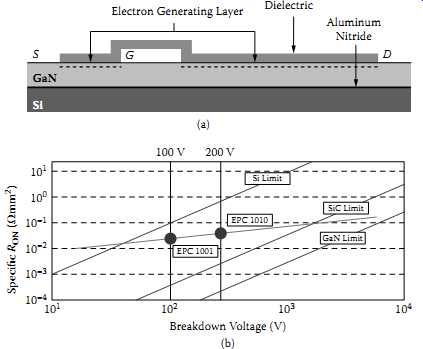
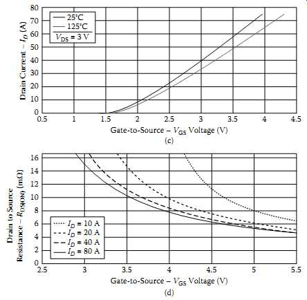
FIG. 34 Some preliminary details on EPC's GaN devices: (a) structure; (b)
theoretical resistance * die area for Si/SiC/GaN, etc.; (c) transfer characteristics;
(d) RDS(on) versus VGS. Electron Generating Layer Dielectric Aluminum Nitride
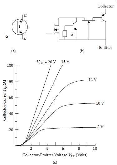
FIG. 35 IGBT: (a) symbol; (b) equivalent circuit; (c) typical output characteristics.
The JFET supports most of the voltage and allows the MOSFET to be a low-voltage type, and consequently have a low RDS(ON) value. The absence of the integral reverse diode gives the user the flexibility of choosing an external fast-recovery diode to match a specific requirement. This feature can be an advantage or a disadvantage, depending on the frequency of operation, cost of diodes, current requirement, etc.
In IGBTs, on-resistance values have been reduced by a factor of about 10 compared with those of conventional n-channel power MOSFETs of comparable size and voltage rating.
IGBT power modules are rapidly gaining applications in systems such as inverters, UPS systems, and automotive environments. The device ratings are reaching beyond 1800 V and 600 A. The frequency limits from early values of 5 kHz are now reaching beyond 20 kHz while intelligent IGBT modules that include diagnostic and control logic along with gate drive circuits are gradually entering the market.
A characteristics comparison of IGBTs, power MOSFETs, bipolars, and Darlingtons is contained in Table 2. References [10-15] provide more details on IGBTs and their applications.
Following is a brief guideline for applying IGBT in practical systems, together with some details from the Advanced Power Technology (APT) application note [58].
State-of-the-art IGBT devices are efficient and less costly, and they are used not only in motor drive-like applications but also in SMPS systems running into a few 100 kHz.
FIG. 36(a) depicts the comparison of similar size MOSFETs versus IGBTs from APT.
From FIG. 36(a) it’s clear that above currents of 15 A, IGBT on-state voltage is much less than a similar-size MOSFET. Also, we can see that temperature has much less impact on the on-state voltage of an IGBT. This kind of performance encourages designers to use IGBTs in high-power SMPS applications.
There are two different types of IGBTs, namely punch-through (PT) devices and non-punch through (NPT) devices. FIG. 36(b) indicates the cross section of a PT-IGBT where the additional n+ buffer layer is present, which does not exist in an NPT device.
Usually an NPT device is preferred in an application such as a motor drive where shortcircuit capability of the device is preferred, while in higher-speed applications such as SMPSs a PT device is attractive. For a given switching speed, an NPT technology generally provides a higher VCE(on) voltage than a PT device. NPT devices are typically shortcircuit rated while PT devices are not.
Given the case that there is a parasitic NPN transistor within an IGBT, this could create the equivalent of thyristor, which is an NPNP device. If this parasitic transistor ever turns on, latch-up can occur. For this reason careful adherence to data sheet values is recommended. FIG. 36(c) indicates a simplified equivalent circuit, and FIG. 36(d) indicates the IGBT model including the parasitic thyristor. In general an IGBT has a longer switching-off period due to long tail current, and this needs to be considered in a design. References [59] and [60] give very useful application information from a designer's viewpoint.
====
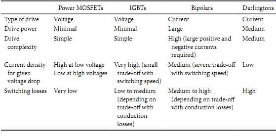
Table 2 Characteristics Comparison of IGBTs, Power MOSFETs, Bipolars, and Darlingtons
Power MOSFETs IGBTs Bipolars Darlingtons Type of drive Voltage; Voltage Current; Current Drive power Minimal; Minimal Large Medium Drive complexity Simple; Simple High (large positive and negative currents required) Medium Current density for given voltage drop High at low voltage Low at high voltages Very high (small trade-off with switching speed) Medium (severe trade-off with switching speed) Low Switching losses Very low; Low to medium (depending on trade-off with conduction losses) Medium to high (depending on trade-off with conduction losses) High
====
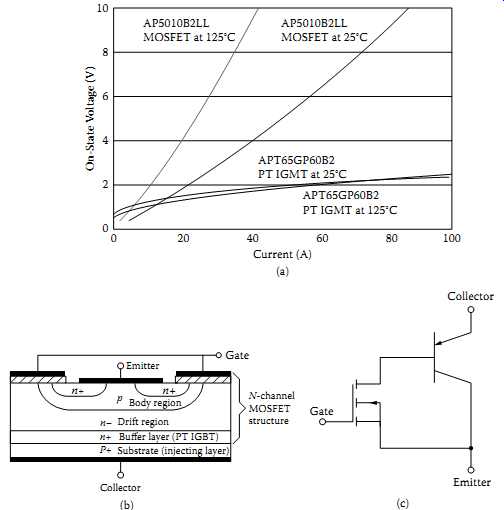
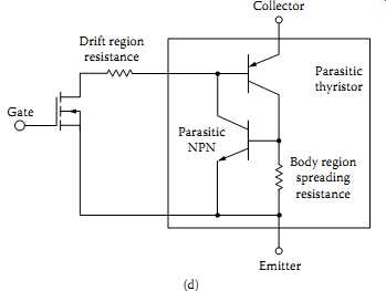
FIG. 36 Practical IGBT devices (a) comparison of similar size MOSFET and
an IGBT (b) cross section of a PT device (c) simplified equivalent circuit
(d) IGBT model showing parasitic thyristor (Sources: Ref[58-59], parts (a)/(d)
reproduced with permission from Power Electronics Technology magazine).
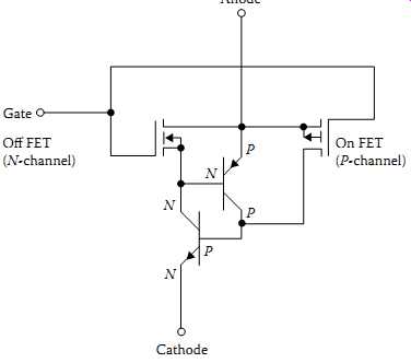
FIG. 37 MCT-equivalent circuit.
MOS-Controlled Thyristor (MCT)
MOS-controlled thyristors are a new class of power semiconductor devices that combine thyristor current and voltage capability with MOS-gated turn-on and turn-off. Various subclasses of MCTs can be made: p-type or n-type, symmetric or asymmetric blocking, one or two-sided Off-FET gate control, and various turn-on alternatives including direct turn-on with light.
All of these subclasses have one thing in common: turn-off is accomplished by turning on a highly interdigitated Off-FET to short out one or both of the thyristor's emitter base junctions. The device, first announced a few years ago by General Electric's power semiconductor operation (later part of Harris Semiconductor, USA), was developed by Vic Temple. Harris was the only supplier of MCTs; however, ABB has introduced a new device called the insulated gate commutated thyristor (IGCT), which is in the same family of devices.
FIG. 37 depicts the MCT equivalent circuit. Most of the characteristics of an MCT can be understood easily by reference to the equivalent circuit shown here. MCT closely approximates a bipolar thyristor (the two-transistor model is shown) with two opposite polarity MOSFET transistors connected between its anode and the proper layers to turn it on and off. Since MCT is an NPNP device rather than a PNPN device, an output terminal or cathode must be negatively biased.
Driving the gate terminal negative with respect to the common terminal or anode turns the P channel FET on, firing the bipolar SCR. Driving the gate terminal positive with respect to the anode turns on the N-channel FET, shunting the base drive to the PNP bipolar transistor making up part of the SCR, causing the SCR to turn off. It’s obvious from the equivalent circuit that when no gate to anode voltage is applied to the gate terminal of the device, the input terminals of the bipolar SCR are unterminated.
Operation without gate bias is not recommended.
In the P-MCT, a P-channel On-FET is turned on with a negative voltage, which charges up the base of the lower transistor to latch on the MCT. The MCT turns on simultaneously over the entire device area, giving the MCT excellent di/dt capability.
FIG. 38 compares different 600 V power-switching devices. FIG. 39 compares the characteristics of a 1000 V P-MCT device with an N-IGBT device of the same voltage rating. Note that the MCT typically has 10 to 15 times the current capability at the same voltage drop.
The MCT will remain in the on state until current is reversed (like a normal thyristor) or until the off-FET is activated by a positive gate voltage. Just as the IGBT looks like a MOSFET driving a BJT, the MCT looks like a MOSFET driving a thyristor (an SCR). SCRs and other thyristors turn on easily, but their turn-off requires stopping, or diverting virtually all of the current flowing through them for a short period of time. On the other hand, the MCT is turned off with voltage control on the high-impedance gate. The MCT offers a lower specific on-resistance at high voltage than any other gate-driven technology.
That is, just as the IGBT operates at a higher current density than the DMOSFET, the MCT (like all thyristors) operates at even higher current densities. In the future, the ultimate power switch may well be the MOS-controlled thyristor (MCT). References [16-20] provide details for designers.
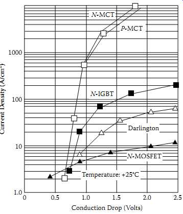
FIG. 38 Comparison of 600 V devices.
MCT as a commercial device was not so popular due to competition from other switching devices. Another new device introduced in early 2000s was the integrated gate commutated thyristor (IGCT) [61]. This is an off-shoot from the GTO technology introduced by ABB.
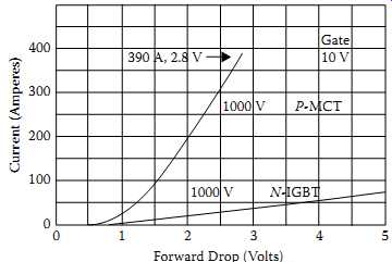
FIG. 39 Comparison of forward voltage drop of 1000 V P-MCT and N-IGBT at
150°C.
References:
- 1. Ashkianazi, G., J. Lorch, and M. Nathan. 1995. Ultrafast GaAs power diodes provide dynamic characteristics with better temperature stability than silicon diodes." PCIM, April, 10-16.
- 2. Hammerton, C. J. 1989. Peak current capability of thyristors. PCIM, November, 52-55.
- 3. Coulbeck, L., W. J. Findlay, and A. D. Millington. 1994. Electrical trade-offs for GTO thyristors. Power Engineering Journal, February, 18-26.
- 4. Bassett, Roger J., and Colin Smith. 1989. A GTO tutorial: Part I. PCIM, July, 35-39.
- 5. Bassett, Roger J., and Colin Smith. 1989. A GTO tutorial: Part II-gate drive. PCIM, August, 21-28.
- 6. McNulty, Tom. 1993. Understanding power MOSFETs. Application Note AN 7244.2, Harris Semiconductor, September.
- 7. Travis, Bill. 1989. Power MOSFETs & IGBTS. EDN, January, 128-47.
- 8. Goodenough, Frank. 1995. Trench-gate DMOSFETs in S0-8 switch 10A at 30 V. Electronic Design, March, 65-77.
- 9. Goodenough, Frank. 1994. DMOSFETs switch milliwatts to megawatts. Electronic Design, September, 57-65.
- 10. Furuhata, Sooichi, and Tadashi Miyasaka. 1990. IGBT power modules challenge bipolars: MOSFETs in invertor applications. PCIM, January, 24-28.
- 11. Russel, J. P., et al. 1997. The IGBTs-a new high conductance MOS-gated device. Application Note AN 8607.1. Harris Semiconductor, May.
- 12. Wojslawowicz, J. E. 1995. Third generation IGBTS approach ideal switch capability. PCIM, January, 28-37.
- 13. Frank, Randy, and John Wertz. 1994. IGBTS integrate protection for distributorless ignition systems. PCIM, February, 42-49.
- 14. Dierberger, K. 1992. IGBT Do's and Don'ts. PCIM, August, 50-55.
- 15. Clemente, S., A. Dubhashi, and B. Pelly. 1990. Improved IGBT process eliminates latch-up, yields higher switching speed-part I. PCIM, October, 8-16.
- 16. Temple, V., D. Watrous, S. Arthur, and P. Kendle. 1992. MOS-controlled thyristor (MCT) power switches-part I: MCT basics. PCIM, November, 9-16.
- 17. Temple, V., D. Watrous, S. Arthur, and P. Kendle. 1993. MOS-controlled thyristor (MCT) power switches-part II: Gate drive and applications. PCIM, January, 24-33.
- 18. Temple, V., D. Watrous, S. Arthur, and P. Kendle. 1993. MOS-controlled thyristor (MCT) power switches-part III: Switching, applications and the future. PCIM, February, 24-33.
- 19. Temple, V. A. K. 1986. MOS-controlled thyristors-a new class of power devices. IEEE Transactions on Electronic Devices ED-33 (10): 1609-18.
- 20. Temple, V. A. K. 1989. Advances in MOS-controlled thyristor technology. PCIM, November, 12-15.
- 21. Burkel, R., and T. Schneider. 1994. Fast recovery epitaxial diodes characteristics- applications-examples. IXYS Technical Information 33 (Publication No. D94004E).
- 22. Williams, B. W. 1992. Power electronics: Devices, drivers, applications and passive components. New York: Macmillan.
- 23. Kinzer, Dan. 1995. Fifth-generation MOSFETs set new benchmarks for low on-resistance. PCIM, August, 59.
- 24. Delaney, S., A. Salih, and C. Lee. 1995. GaAs diodes improve efficiency of 500 kHz DC-DC converter. PCIM, August, 10-11.
- 25. Deuty, S. 1996. GaAs rectifiers offer high efficiency in a 1 MHz 400 Vdc to 48 Vdc converter. HFPC Conference Proceedings, September, 24-35.
- 26. Davis, C. 1997. Integrated power MOSFET and Schottky diode improves power supply designs. PCIM, January, 10-14.
- 27. Goodenough, Frank. 1997. Dense MOSFET enables portable power control. Electronic Design, April 14, 45-50.
- 28. Peter, J. M. 1989. High frequency power rectification. PCIM, April, 24-38.
- 29. Peter, J. M. 1984. Switching behavior of fast diodes in the converter circuits. Power Conversion International, September, 64-70.
- 30. Boreneman, E. H. 1977. Choosing the correct recovery rectifier. Solid State Power Conversion, November/December, 14-16.
- 31. Anderson, S., K. Gauen, and W. C. Roman. 1991. Low loss, low noise diodes improve high frequency power supplies, part II. PCIM, March, 39-42.
- 32. Carsten, B. 1986. Reverse recovery characteristics of high speed rectifiers. PCIM, February, 42-48.
- 33. Lauritzen, P. O., and C. L. Ma. 1991. A simple diode model with reverse recovery. IEEE Transcations on Power Electronics 6 (2, April): 188-91.
- 34. Chiola, D. 2002. Trench technology boosts Schottky rectifier. Power Electronics Technology, December, 32-34.
- 35. Chen, M., H. Kuo, and K. Sweetman. 2006. High-voltage TMBS diodes challenge planar Schottkys. Power Electronics Technology, October, 22-32.
- 36. Kapels, H., M. Krach, et al. 2002. SiC Schottky diodes ready for blast off. Power Electronics Technology, January, 15-21.
- 37. Zverev, I. 2003. SiC Schottky diodes improve boost converter performance. Power Electronics Technology, March, 38-49.
- 38. O'Neill, M. 2005. SiC puts new spin on motor drives. Power Electronics Technology, January, 14-22.
- 39. Hodge, S. 2004. SiC Schottky diodes in power factor correction. Power Electronics Technology, August, 14-22.
- 40. Cooper, J. A. 1998. Advances in silicon carbide power switching devices. Proceedings of Power Electronics, November, 235-45.
- 41. Barkhordarian, V. 1996. Power MOSFET basics. PCIM, June, 28-36.
- 42. Giovanni, F. D. 1998. Mesh overlay MOSFET. PCIM, May, 50-56.
- 43. Ronan, H. R. 1998. MOSFET SOA-thermal current focussing affects power MOSFET operation. PCIM, August, 51-55.
- 44. Ronan, H. R. 1997. One equation quantifies a power MOSFET's UIS rating. PCIM, August, 26-35.
- 45. Hammerton, C. J. 1996. Avalanche overshot poses a hazard for MOSFETs. PCIM, January, 52-56.
- 46. Ronan, H. R. 1998. Power rectifier unclamped inductive switching. PCIM, October, 16-24.
- 47. Wu, T., H. Tran, and C. Nguyen. 2000. Dynamic stresse scan cause power MOSFET failure. PCIM, April, 28-44.
- 48. Blake, C., T. McDonald, D. Kinzer, et al. 2005. Evaluating the reliability of power MOSFETS. Power Electronics Technology, November, 40-44.
- 49. Kazmirski, T. 2006. Protecting MOSFETS against overcurrent events. Power Electronics Technology, January, 14-21.
- 50. Benczkowski, S., and R. Mancini. 1998. Improved MOSFET model. PCIM, September, 64-68.
- 51. Pandya, K. 2007. Tool eases modelling of power MOSFETs. Power Electronics Technology, March, 30-33.
- 52. Pearson, S. S. Tran, and S. Sapp. 2007. Improved MOSFET model achieves higher accuracy. Power Electronics Technology, January, 14-19.
- 53. Moxey, G. 2003. TrenchFETs enhance DC-DC converter performance. Power Electronics Technology, February, 36-38.
- 54. Hancock, M. 2005. Superjunction FETS boost efficiency in PWMs. Power Electronics Technology, July, 20-29.
- 55. Davis, S. 2010. Enhancement mode GaN MOSFET delivers impressive performance. Power Electronics Technology, March, 10-13.
- 56. Davis, S. 2010. GaN powers MOSFET figure of Merit past silicon-based devices. Power Electronics Technology, March,14-17.
- 57. Alderman, A. N. 2010. Where are the high voltage GaN products? Power Electronics Technology, June, 34-38.
- 58. Dodge, J., and J. Hess. 2002. IGBT tutorial. Application Note APT0201, rev. B. Advanced Power Technology, July 1.
- 59. Dodge, J. 2003. Why opt for IGBTs in SMPS applications? Power Electronics Technology, July, 34-39.
- 60. McArthur, R. 2001. Making use of gate charge information in MOSFET and IGBT data sheets. Application Note APT0103, rev. B. Advanced Power Technology, October.
- 61. Carroll, E., and J. Siefgken. 2002. IGCTs: Moving on the right track. Power Electronics Technology, August, 16-22.
Bibliography:
- Anderson, S., K. Gauen, and C. W. Roman. "Low Loss, Low Noise Diodes Improve High Frequency Power Supplies." PCIM, February 1991, 6-13.
- Adler, Michael, et al. "The Evolution of Power Device Technology." IEEE Transactions on Electronic Devices, ED-31, no. 11 (November 1984): 1570-91.
- Arthur, S. D., and V. A. K. Temple. "Special 1400 Volt N-MCT Designed for Surge Applications." Proceedings of EPE '93 2 (1993): 266-71.
- Barkhordarian, V. "Power MOSFET Basics." PCIM, June 1996, 28-39.
- Bird, B. M., K. G. King, and D. A. G. Pedder. An Introduction to Power Electronics, 2nd ed. (New York: Wiley, 1993).
- Borras, R., P. Aloisi, and D. Shumate. "Avalanche Capability of Today's Power Semiconductors." Proceedings of EPE '93 2 (1993): 167-71.
- Bose B. K. Modern Power Electronics (New York: IEEE Press, 1997).
- Bradley, D. A. Power Electronics (London: Chapman & Hall, 1995).
- Consoli, A., et al. "On the Selection of IGBT Devices in Soft Switching Applications." Proceedings of EPE '93 (1993): 337-43.
- Deuty, Scott, Emory Carter, and Ali Salih. 1995. "GaAs Diodes Improve Power Factor Correction Boost Converter Performance." PCIM, January, 8-19.
- Driscoll, J. 1990. "Bipolar Transistors and High Side Switches in High Voltage, High Frequency Power Supplies." Proceedings of Power Conversion Conference, October.
- Driscoll, J. C. 1990. "High Current Fast Turn-On Pulse Generation Using Power Tech PG-5xxx Series of 'Pulser' Gate Assisted Turn-Off Thyristors (GATO's)." Power Tech App Note.
- Eckel, H. G., and L. Sack. 1993. "Optimization of the Turn-Off Performance of IGBT at Overcurrent and Short-Circuit Current." Proceedings of EPE '93, 317-21.
- Frank, Randy, and Richard Valentine. 1990. "Power FETS Cope with the Automotive Environment." PCIM, February, 33-39.
- Gauen, K., and W. Chavez. 1993. "High Cell Density MOSFETs: Low on Resistance Affords New Design Options." Proceedings of PCI, October, 254-64.
- Goodenough, Frank. 1994. "DMOSFETs, IGBTS Switch High Voltage." Electronic Design 7 (November): 95-105.
- Heumann, K., and M. Quenum. 1993. "Second Breakdown and Latch-Up Behavior of IGBTs." Proceedings of EPE '93, 301-5.
- International Rectifier. 1997. Schottky Diode Designer's Manual.
- Lynch, Fernando. 1994. "Two terminal power semiconductor technology breaks current/ voltage/power barrier." PCIM, October, 10-14.
- Locher, R. E. 1996. "1600V BIMOSFET Transistors Expand High Voltage Applications." PCIM, August, 8-21.
- Mitlehner, H., and H. J. Schulze. 1994. "Current Developments in High Power Thyristors." EPE Journal 4 (1, March): 36-47.
- Mitter, C. S. 1995. "Introduction to IGBTs." PCIM, December, 32-39.
- Mohan, N., T. M. Undeland, and W. P. Robbins. 1989. Power Electronics: Converter, Applications, and Design ( New York: Wiley).
- Nilsson, T. 1986. "The Insulated Gate Bipolar Transistor Response in Different Short Circuit Situations." Proceedings of EPE '93, 328-31.
- Peter, Jean Marie. 1986. "State of the Art and Development in the Field of Medium Power Devices." PCIM, May, 14-27.
- Polner, Alex. 1995. "Characteristics of ultra High Power Transistors." Proceedings of First National Solid State Power Conversion Conference, March.
- Ramshaw, R. S. 1993. Power Electronics Semiconductor Switches ( London: Chapman & Hall).
- Rippel, Wally E. 1989. "MCT/FET Composite Switch: Big Performance with Small Silicon." PCIM, November, 16-27.
- Roehr, Bill. 1989. "Power Semiconductor Mounting Considerations." PCIM, September, 8-18.
- Sasada, Yorimichi, Shigeki Morita, and Makato Hideshima. 1986. "High Voltage, High Speed IGBT Transistor Modules." Toshiba Review 157 (Autumn): 34-38.
- Schultz, Warren. 1985. "Ultrafast-Recovery Diodes Extend the SOA of Bipolar Transistors." Electronic Design 14 (March): 167-74.
- Serverns, Rudy, and Jack Armijos. 1984. MOSPOWER Applications Handbook. Siliconix Inc.
- Smith, Colin, and Roger Bassett. 1989. "GTO Tutorial Part III-Power Loss in Switching Applications." PCIM, September, 99-105.
- Travis, B. 1996. "MOSFETs and IGBTs Differ in Drive Methods and Protections Needs." EDN, March 1, 123-37.