AMAZON multi-meters discounts AMAZON oscilloscope discounts
OUTLINE
- 1. Amplifier Operation
- 2. Transistor AC Models
- 3. The Common-Emitter Amplifier
- 4. The Common-Collector Amplifier
- 5. The Common-Base Amplifier
- 6. Multistage Amplifiers
- 7. The Differential Amplifier
- 8. Troubleshooting
- Application Activity
- GreenTech Application 6: Wind Power
OBJECTIVES
-- Describe amplifier operation
-- Discuss transistor models
-- Describe and analyze the operation of common-emitter amplifiers
-- Describe and analyze the operation of common-collector amplifiers
-- Describe and analyze the operation of common-base amplifiers
-- Describe and analyze the operation of multistage amplifiers
-- Discuss the differential amplifier and its operation
-- Troubleshoot amplifier circuits
TERMINOLOGY
-- r parameter
-- Common-emitter
-- ac ground
-- Input resistance
-- Output resistance
-- Attenuation
-- Bypass capacitor
-- Common-collector
-- Emitter-follower
-- Common-base
-- Decibel
-- Differential amplifier
-- Common mode
-- CMRR (Common-mode rejection ratio)
APPLICATION ACTIVITY PREVIEW
The Application Activity in this section involves a preamplifier circuit for a public address system. The complete system includes the preamplifier, a power amplifier, and a dc power supply. You will focus on the preamplifier in this section and then on the power amplifier in Section 7.
INTRODUCTION
The things you learned about biasing a transistor in Section 5 are now applied in this section where bipolar junction transistor (BJT) circuits are used as small-signal amplifiers.
The term small-signal refers to the use of signals that take up a relatively small percentage of an amplifier's operational range. Additionally, you will learn how to reduce an amplifier to an equivalent dc and ac circuit for easier analysis, and you will learn about multistage amplifiers. The differential amplifier is also covered.
1. AMPLIFIER OPERATION
The biasing of a transistor is purely a dc operation. The purpose of biasing is to establish a Q-point about which variations in current and voltage can occur in response to an ac input signal. In applications where small signal voltages must be amplified--such as from an antenna or a microphone-variations about the Q-point are relatively small. Amplifiers designed to handle these small ac signals are often referred to as small-signal amplifiers.
After completing this section, you should be able to:
-- Describe amplifier operation
-- Identify ac quantities
-- Distinguish ac quantities from dc quantities
-- Discuss the operation of a linear amplifier
-- Define phase inversion
-- Graphically illustrate amplifier operation
-- Analyze ac load line operation
HISTORY NOTE:
The American inventor Lee De Forest (1873-1961) is one of several pioneers of radio development. De Forest experimented with receiving long distance radio signals and in 1907 patented an electronic device named the audion, which was the first amplifier. De Forest's new three-electrode (triode) vacuum tube boosted radio waves as they were received and made possible what was then called "wireless telephony," which allowed the human voice, music, or any broadcast signal to be heard.
AC Quantities
In the previous sections, dc quantities were identified by nonitalic uppercase (capital) sub scripts such as IC, IE, VC, and VCE. Lowercase italic subscripts are used to indicate ac quantities of rms, peak, and peak-to-peak currents and voltages: for example, Ic, Ie, Ib, Vc, and Vce (rms values are assumed unless otherwise stated). Instantaneous quantities are represented by both lowercase letters and subscripts such as ic, ie, ib, and vce. FIG. 1 illustrates these quantities for a specific voltage waveform.
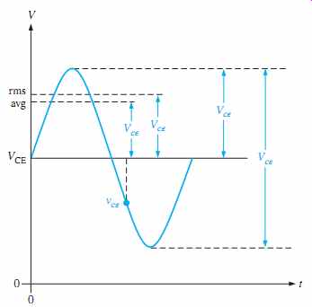
FIG. 1 Vce can represent rms, average, peak, or peak-to-peak, but rms
will be assumed unless stated otherwise. vce can be any instantaneous value
on the curve.
In addition to currents and voltages, resistances often have different values when a circuit is analyzed from an ac viewpoint as opposed to a dc viewpoint. Lowercase subscripts are used to identify ac resistance values. For example, Rc is the ac collector resistance, and RC is the dc collector resistance. You will see the need for this distinction later. Resistance values internal to the transistor use a lowercase r’ to show it is an ac resistance. An example is the internal ac emitter resistance, r’e.
The Linear Amplifier
A linear amplifier provides amplification of a signal without any distortion so that the out put signal is an exact amplified replica of the input signal. A voltage-divider biased transistor with a sinusoidal ac source capacitively coupled to the base through C1 and a load capacitively coupled to the collector through C2 is shown in FIG. 2. The coupling capacitors block dc and thus prevent the internal source resistance, Rs, and the load resistance, RL, from changing the dc bias voltages at the base and collector. The capacitors ideally appear as shorts to the signal voltage. The sinusoidal source voltage causes the base voltage to vary sinusoidally above and below its dc bias level, VBQ. The resulting variation in base current produces a larger variation in collector current because of the current gain of the transistor.
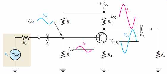
FIG. 2 An amplifier with voltage-divider bias driven by an ac voltage
source with an internal resistance, Rs.
As the sinusoidal collector current increases, the collector voltage decreases. The collector current varies above and below its Q-point value, ICQ, in phase with the base current.
The sinusoidal collector-to-emitter voltage varies above and below its Q-point value, VCEQ, 180° out of phase with the base voltage, as illustrated in FIG. 2. A transistor always produces a phase inversion between the base voltage and the collector voltage.
A Graphical Picture
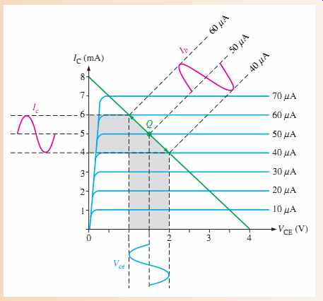
The operation just described can be illustrated graphically on the ac load line, as shown in FIG. 3. The sinusoidal voltage at the base produces a base current that varies above and below the Q-point on the ac load line, as shown by the arrows.
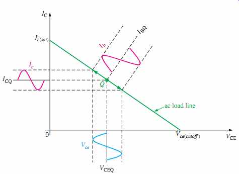
FIG. 3 Graphical ac load line operation of the amplifier showing the variation
of the base current, collector current, and collector-to-emitter voltage
about their dc Q-point values. Ib and Ic are on different scales.
Lines projected from the peaks of the base current, across to the IC axis, and down to the VCE axis, indicate the peak-to-peak variations of the collector current and collector-to emitter voltage, as shown. The ac load line differs from the dc load line because the effective ac collector resistance is RL in parallel with RC and is less than the dc collector resistance RC alone. This difference between the dc and the ac load lines is covered in Section 7 in relation to power amplifiers.
---------------
EXAMPLE 1
The ac load line operation of a certain amplifier extends 10 uA above and below the Q-point base current value of 50 uA as shown in FIG. 4. Determine the resulting peak-to-peak values of collector current and collector-to-emitter voltage from the graph.
Solution:
Projections on the graph of FIG. 4 show the collector current varying from 6 mA to 4 mA for a peak-to-peak value of 2 mA and the collector-to-emitter voltage varying from 1 V to 2 V for a peak-to-peak value of 1 V.
---------------
SECTION 1 CHECKUP
1. When Ib is at its positive peak, Ic is at its __ peak, and Vce is at its _ peak.
2. What is the difference between VCE and Vce?
3. What is the difference between Re and r’ e?
2. TRANSISTOR AC MODELS
To visualize the operation of a transistor in an amplifier circuit, it is often useful to represent the device by a model circuit. A transistor model circuit uses various internal transistor parameters to represent its operation. Transistor models are described in this section based on resistance or r parameters. Another system of parameters, called h parameters, is briefly described.
After completing this section, you should be able to:
-- Discuss transistor models
-- List and define the r parameters
-- Describe the r-parameter transistor model
-- Determine re _ using a formula
-- Compare ac beta and dc beta
-- List and define the h parameters
r Parameters
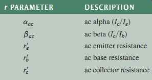
The five r parameters commonly used for BJTs are given in TABLE 1. The italic lowercase letter r with a prime denotes resistances internal to the transistor.
r-Parameter Transistor Model
An r-parameter model for a BJT is shown in FIG. 5(a). For most general analysis work, it can be simplified as follows: The effect of the ac base resistance (r’ b) is usually small enough to neglect, so it can be replaced by a short. The ac collector resistance (r’ c) is usually several hundred kilohms and can be replaced by an open. The resulting simplified r-parameter equivalent circuit is shown in FIG. 5(b).
The interpretation of this model circuit in terms of a transistor's ac operation is as follows: A resistance (r’ e) appears between the emitter and base terminals. This is the resistance "seen" looking into the emitter of a forward-biased transistor. The collector effectively acts as a dependent current source of αac Ie or, equivalently, βac Ib, represented by the diamond-shaped symbol. These factors are shown with a transistor symbol in FIG. 6.
Determining r’e by a Formula
For amplifier analysis, the ac emitter resistance r’ e, is the most important of the r parameters. To calculate the approximate value of r’e you can use EQN. 1, which is derived assuming an abrupt junction between the n and p regions. It is also temperature dependent and is based on an ambient temperature of 20°C.
The numerator will be slightly larger for higher temperatures or transistors with a gradual (instead of an abrupt) junction. Although these cases will yield slightly different results, most designs are not critically dependent on the value of r’e and you will generally obtain excellent agreement with actual circuits using the equation as given.
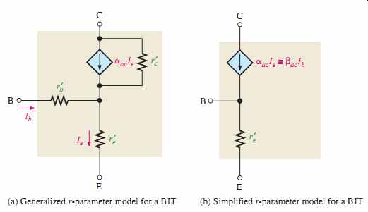
FIG. 5 r-parameter transistor model.
(a) Generalized r-parameter model for a BJT (b) Simplified r-parameter model for a BJT
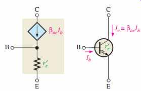
FIG. 6 Relation of transistor symbol to r-parameter model.
Comparison of the AC Beta (Beta ac) to the DC Beta ( Beta DC)
For a typical transistor, a graph of IC versus IB is nonlinear, as shown in FIG. 7(a). If you pick a Q-point on the curve and cause the base current to vary an amount delta_IB then the collector current will vary an amount delta_IC as shown in part (b). At different points on the nonlinear curve, the ratio delta_IC/delta_IB will be different, and it may also differ from the IC IB ratio at the Q-point. Since βDC = IC/IB and βac =delta_IC/delta_IB, the values of these two quantities can differ slightly.
FIG. 7 IC-versus-IB curve illustrates the difference between βDC = IC/IB and Bac = delta_IC/delta_IB.
h Parameters
A manufacturer's datasheet typically specifies h (hybrid) parameters (hi, hr, hf, and ho) be cause they are relatively easy to measure.
The four basic ac h parameters and their descriptions are given in TABLE 2. Each of the four h parameters carries a second subscript letter to designate the common-emitter (e), common-base (b), or common-collector (c) amplifier configuration, as listed in TABLE 3.
The term common refers to one of the three terminals (E, B, or C) that is referenced to ac ground for both input and output signals. The characteristics of each of these three BJT amplifier configurations are covered later in this section.

TABLE 2 Basic ac h parameters.
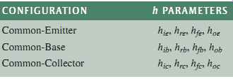
TABLE 3 Subscripts of h parameters for each of the three amplifier configurations.
Relationships of h Parameters and r Parameters The ac current ratios, aac and bac, convert directly from h parameters as follows:
αac = hfb
βac = hfe
Because datasheets often provide only common-emitter h parameters, the following formulas show how to convert them to r parameters. We will use r parameters throughout the text because they are easier to apply and more practical.
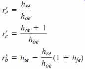
SECTION 2 CHECKUP
1. Define each of the parameters: αac, βac, r’ e, r’ b, and r’ c.
2. Which h parameter is equivalent to βac?
3. If IE = 15 mA, what is the approximate value of r’ e?
3 THE COMMON-EMITTER AMPLIFIER
As you have learned, a BJT can be represented in an ac model circuit. Three amplifier configurations are the common-emitter, the common-base, and the common-collector.
The common-emitter (CE) configuration has the emitter as the common terminal, or ground, to an ac signal. CE amplifiers exhibit high voltage gain and high current gain.
The common-collector and common-base configurations are covered in the sections 4 and 5.
After completing this section, you should be able to:
-- Describe and analyze the operation of common-emitter amplifiers
-- Discuss a common-emitter amplifier with voltage-divider bias
-- Show input and output signals
-- Discuss phase inversion
-- Perform a dc analysis
-- Represent the amplifier by its dc equivalent circuit
-- Perform an ac analysis
-- Represent the amplifier by its ac equivalent circuit
-- Define ac ground
-- Discuss the voltage at the base
-- Discuss the input resistance at the base and the output resistance
-- Analyze the amplifier for voltage gain
-- Define attenuation
-- Define bypass capacitor
-- Describe the effect of an emitter bypass capacitor on voltage gain
-- Discuss voltage gain without a bypass capacitor
-- Explain the effect of a load on voltage gain
-- Discuss the stability of the voltage gain
-- Define stability
-- Explain the purpose of swamping r’ e and the effect on input resistance
-- Determine current gain and power gain
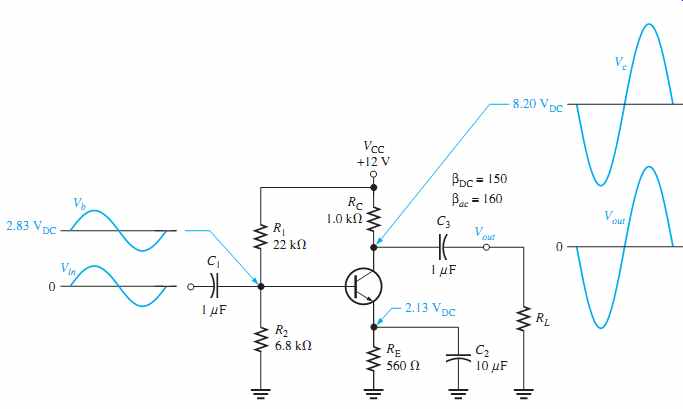
FIG. 8 A common-emitter amplifier.
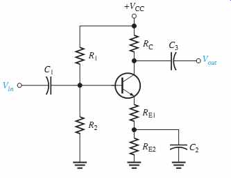
FIG. 8 shows a common-emitter amplifier with voltage-divider bias and coupling capacitors C1 and C3 on the input and output and a bypass capacitor, C2, from emitter to ground. The input signal, Vin, is capacitively coupled to the base terminal, the output signal, Vout, is capacitively coupled from the collector to the load. The amplified output is out of phase with the input. Because the ac signal is applied to the base terminal as 180° the input and taken from the collector terminal as the output, the emitter is common to both the input and output signals. There is no signal at the emitter because the bypass capacitor effectively shorts the emitter to ground at the signal frequency. All amplifiers have a combination of both ac and dc operation, which must be considered, but keep in mind that the common-emitter designation refers to the ac operation.
Phase Inversion
The output signal is out of phase with the input signal. As the input signal voltage changes, it causes the ac base current to change, resulting in a change in the collector current from its Q-point value. If the base current increases, the collector current increases above its Q-point value, causing an increase in the voltage drop across RC. This increase in the voltage across RC means that the voltage at the collector decreases from its Q-point. So, any change in input signal voltage results in an opposite change in collector signal voltage, which is a phase inversion.
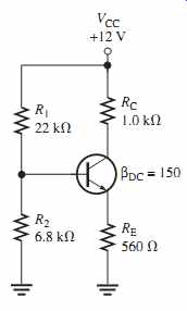
FIG. 9 DC equivalent circuit for the amplifier in FIG. 8.
DC Analysis
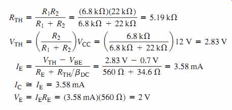
To analyze the amplifier in FIG. 8, the dc bias values must first be determined. To do this, a dc equivalent circuit is developed by removing the coupling and bypass capacitors because they appear open as far as the dc bias is concerned. This also removes the load resistor and signal source. The dc equivalent circuit is shown in FIG. 9.
Theveninizing the bias circuit and applying Kirchhoff's voltage law to the base-emitter circuit, 180°
AC Analysis
To analyze the ac signal operation of an amplifier, an ac equivalent circuit is developed as follows:
1. The capacitors C1, C2, and C3 are replaced by effective shorts because their values are selected so that XC is negligible at the signal frequency and can be considered to be 0-Ω.
2. The dc source is replaced by ground.
A dc voltage source has an internal resistance of near 0-Ω because it holds a constant volt age independent of the load (within limits); no ac voltage can be developed across it so it appears as an ac short. This is why a dc source is called an ac ground.
The ac equivalent circuit for the common-emitter amplifier in FIG. 8 is shown in FIG. 10(a). Notice that both RC and R1 have one end connected to ac ground (red) be cause, in the actual circuit, they are connected to VCC which is, in effect, ac ground.
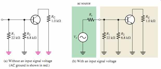
FIG. 10 AC equivalent circuit for the amplifier in FIG. 8. (a) Without
an input signal voltage (AC ground is shown in red.) (b) With an input
signal voltage
In ac analysis, the ac ground and the actual ground are treated as the same point electrically. The amplifier in FIG. 8 is called a common-emitter amplifier because the bypass capacitor C2 keeps the emitter at ac ground. Ground is the common point in the circuit.
Signal (AC) Voltage at the Base
An ac voltage source, Vs, is shown connected to the input in FIG. 10(b). If the internal resistance of the ac source is 0-Ω, then all of the source voltage appears at the base terminal. If, however, the ac source has a nonzero internal resistance, then three factors must be taken into account in determining the actual signal voltage at the base. These are the source resistance (Rs), the bias resistance (R1 || R2), and the ac input resistance at the base of the transistor (Rin(base)). This is illustrated in FIG. 11(a) and is simplified by combining R1, R2, and Rin(base) in parallel to get the total input resistance, Rin(tot), which is the resistance "seen" by an ac source connected to the input, as shown in FIG. 11(b). A high value of input resistance is desirable so that the amplifier will not excessively load the signal source. This is opposite to the requirement for a stable Q-point, which requires smaller resistors. The conflicting requirement for high input resistance and stable biasing is but one of the many trade-offs that must be considered when choosing components for a circuit. The total input resistance is expressed by the following formula:
EQN. 2 Rin(tot) = R1 || R2 || Rin(base)
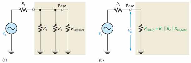
FIG. 11 AC equivalent of the base circuit.
As you can see in the figure, the source voltage, Vs, is divided down by Rs (source resistance) and Rin(tot) so that the signal voltage at the base of the transistor is found by the volt age-divider formula as follows:

Input Resistance at the Base
To develop an expression for the ac input resistance looking in at the base, use the simplified r-parameter model of the transistor. FIG. 12 shows the transistor model connected to the external collector resistor, RC. The input resistance looking in at the base is:
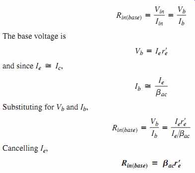
EQN. 3
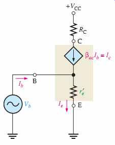
FIG. 12 r-parameter transistor model (inside shaded block) connected
to external circuit.
Output Resistance
The output resistance of the common-emitter amplifier is the resistance looking in at the collector and is approximately equal to the collector resistor.
Rout = RC
Actually, Rout = RC || r’c, but since the internal ac collector resistance of the transistor, r’c, is typically much larger than RC, the approximation is usually valid.
Voltage Gain
The ac voltage gain expression for the common-emitter amplifier is developed using the model circuit in FIG. 14. The gain is the ratio of ac output voltage at the collector (Vc) to ac input voltage at the base (Vb).
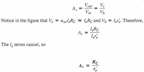
EQN. 5
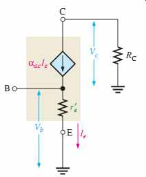
FIG. 14 Model circuit for obtaining ac voltage gain.
EQN. 5 is the voltage gain from base to collector. To get the overall gain of the amplifier from the source voltage to collector, the attenuation of the input circuit must be included.
Attenuation is the reduction in signal voltage as it passes through a circuit and corresponds to a gain of less than 1. For example, if the signal amplitude is reduced by half, the attenuation is 2, which can be expressed as a gain of 0.5 because gain is the reciprocal of attenuation. Suppose a source produces a 10 mV input signal and the source resistance combined with the load resistance results in a 2 mV output signal. In this case, the attenuation is 10 mV / 2 mV = 5. That is, the input signal is reduced by a factor of 5. This can be expressed in terms of gain as 1/5 = 0.2.
Assume that the amplifier in FIG. 15 has a voltage gain from base to collector of Av and the attenuation from the source to the base is Vs/Vb. This attenuation is produced by the source resistance and total input resistance of the amplifier acting as a voltage divider and can be expressed as:

The overall voltage gain of the amplifier, A’v, is the voltage gain from base to collector, Vc/Vb, times the reciprocal of the attenuation, Vb/Vs.

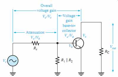
FIG. 15 Base circuit attenuation and overall voltage gain.
Effect of the Emitter Bypass Capacitor on Voltage Gain
The emitter bypass capacitor, which is C2 in FIG. 8, provides an effective short to the ac signal around the emitter resistor, thus keeping the emitter at ac ground, as you have seen. With the bypass capacitor, the gain of a given amplifier is maximum and equal to RC/r’e.
The value of the bypass capacitor must be large enough so that its reactance over the frequency range of the amplifier is very small (ideally 0 Ω) compared to RE. A good rule-of-thumb is that the capacitive reactance, XC, of the bypass capacitor should be at least 10 times smaller than RE at the minimum frequency for which the amplifier must operate.
10Xc <= RE
Voltage Gain Without the Bypass Capacitor
To see how the bypass capacitor affects ac voltage gain, let's remove it from the circuit in FIG. 16 and compare voltage gains.
Without the bypass capacitor, the emitter is no longer at ac ground. Instead, RE is seen by the ac signal between the emitter and ground and effectively adds to r’ e in the voltage gain formula.
The effect of RE is to decrease the ac voltage gain.
Effect of a Load on the Voltage Gain
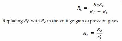
A load is the amount of current drawn from the output of an amplifier or other circuit through a load resistance. When a resistor, RL, is connected to the output through the coupling capacitor C3, as shown in FIG. 17(a), it creates a load on the circuit. The collector resistance at the signal frequency is effectively RC in parallel with RL. Remember, the upper end of RC is effectively at ac ground. The ac equivalent circuit is shown in FIG. 17(b). The total ac collector resistance is
EQN. 7
When Rc <RC because of RL, the voltage gain is reduced. However, if RL >> RC then , Rc = RC and the load has very little effect on the gain.
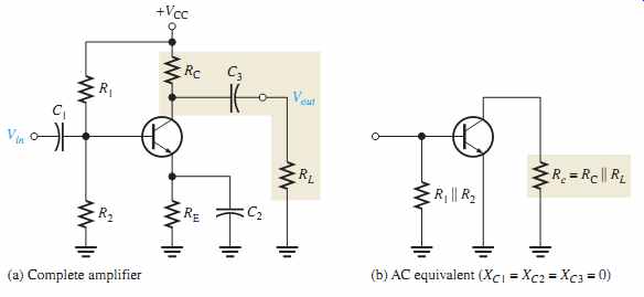
FIG. 17 A common-emitter amplifier with an ac (capacitively) coupled load.
A swamped amplifier uses a partially bypassed emitter resistance to minimize the effect of r_ e on the gain in order to achieve gain stability.
Stability of the Voltage Gain
Stability is a measure of how well an amplifier maintains its design values over changes in temperature or for a transistor with a different Beta.
Although bypassing RE does produce the maximum voltage gain, there is a stability problem because the ac voltage gain is dependent on r’ e since Av = RC/r’e.
Also, r’ e depends on IE and on temperature. This causes the gain to be unstable over changes in temperature because when r’e increases, the gain decreases and vice versa.
With no bypass capacitor, the gain is decreased because RE is now in the ac circuit (Av = RC/(r’e + RE)).
However, with RE unbypassed, the gain is much less dependent on
If the gain is essentially independent of because:
Av = RC / RE
Swamping r’ e to Stabilize the Voltage Gain
Swamping is a method used to minimize the effect of without reducing the voltage gain to its minimum value. This method "swamps" out the effect of on the voltage gain. Swamping is, in effect, a compromise between having a bypass capacitor across RE and having no bypass capacitor at all.
In a swamped amplifier, RE is partially bypassed so that a reasonable gain can be achieved, and the effect of r’ e on the gain is greatly reduced or eliminated. The total external emitter resistance, RE, is formed with two separate emitter resistors, RE1 and RE2, as indicated in FIG. 18. One of the resistors, RE2, is bypassed and the other is not.
Both resistors (RE1 + RE2) affect the dc bias while only RE1 affects the ac voltage gain.
Av = RC / [r’e + RE1]
If RE1 is at least ten times larger than then the effect of is minimized and the approximate voltage gain for the swamped amplifier is r’ e r’ e,
EQN. 8
Av =RC / RE1
The Effect of Swamping on the Amplifier's Input Resistance
The ac input resistance, looking in at the base of a common-emitter amplifier with RE completely bypassed, is Rin = βac r’e. When the emitter resistance is partially bypassed, the portion of the resistance that is unbypassed is seen by the ac signal and results in an increase in the ac input resistance by appearing in series with The formula is r’e.
Current Gain
The current gain from base to collector is However, the overall current gain of the common-emitter amplifier is Ic/Ib or βac.

EQN. 10
Is is the total signal input current produced by the source, part of which (Ib) is base current and part of which (Ibias) goes through the bias circuit (R1 || R2), as shown in FIG. 24. The source "sees" a total resistance of The total current produced by the source is Rs + Rin(tot).

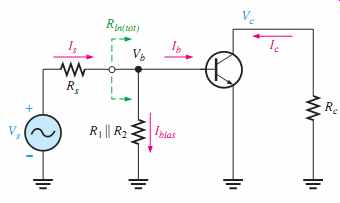
FIG. 24 Signal currents (directions shown are for the positive half-cycle
of Vs ).
Power Gain
The overall power gain is the product of the overall voltage gain (A’v) and the overall current gain (A1).
Ap = A’v Ai
where A’v = Vc/Vs.
SECTION 3 CHECKUP
1. In the dc equivalent circuit of an amplifier, how are the capacitors treated?
2. When the emitter resistor is bypassed with a capacitor, how is the gain of the amplifier affected?
3. Explain swamping.
4. List the elements included in the total input resistance of a common-emitter amplifier.
5. What elements determine the overall voltage gain of a common-emitter amplifier?
6. When a load resistor is capacitively coupled to the collector of a CE amplifier, is the voltage gain increased or decreased?
7. What is the phase relationship of the input and output voltages of a CE amplifier?
