AMAZON multi-meters discounts AMAZON oscilloscope discounts
<< continued from part 1
4. THE COMMON-COLLECTOR AMPLIFIER
The common-collector (CC) amplifier is usually referred to as an emitter-follower (EF). The input is applied to the base through a coupling capacitor, and the output is at the emitter. The voltage gain of a CC amplifier is approximately 1, and its main advantages are its high input resistance and current gain.
After completing this section, you should be able to:
-- Describe and analyze the operation of common-collector amplifiers
-- Discuss the emitter-follower amplifier with voltage-divider bias
-- Analyze the amplifier for voltage gain
-- Explain the term emitter-follower
-- Discuss and calculate input resistance
-- Determine output resistance
-- Determine current gain
-- Determine power gain
-- Describe the Darlington pair
-- Discuss an application
-- Discuss the Sziklai pair
An emitter-follower circuit with voltage-divider bias is shown in FIG. 25. Notice that the input signal is capacitively coupled to the base, the output signal is capacitively coupled from the emitter, and the collector is at ac ground. There is no phase inversion, and the output is approximately the same amplitude as the input.
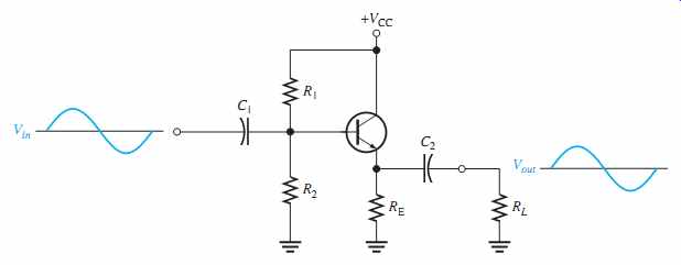
FIG. 25 Emitter-follower with voltage-divider bias.
Voltage Gain
As in all amplifiers, the voltage gain is Av = Vout/Vin. The capacitive reactances are assumed to be negligible at the frequency of operation. For the emitter-follower, as shown in the ac model in FIG. 26,

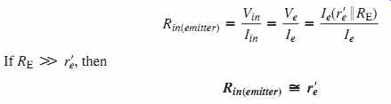
where Re is the parallel combination of RE and RL. If there is no load, then Re=RE. Notice that the gain is always less than 1. If then a good approximation is Re >> r’ e,
EQN. 12
Av = 1
Since the output voltage is at the emitter, it is in phase with the base voltage, so there is no inversion from input to output. Because there is no inversion and because the voltage gain is approximately 1, the output voltage closely follows the input voltage in both phase and amplitude; thus the term emitter-follower.
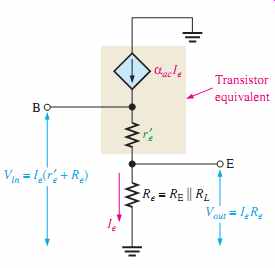
FIG. 26 Emitter-follower model for voltage gain derivation.
Input Resistance
The emitter-follower is characterized by a high input resistance; this is what makes it a useful circuit. Because of the high input resistance, it can be used as a buffer to minimize loading effects when a circuit is driving a low-resistance load. The derivation of the input resistance, looking in at the base of the common-collector amplifier, is similar to that for the common-emitter amplifier. In a common-collector circuit, however, the emitter resistor is never bypassed because the output is taken across Re, which is RE in parallel with RL.
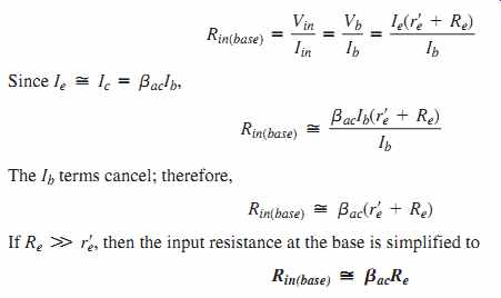
EQN. 13
Output Resistance
With the load removed, the output resistance, looking into the emitter of the emitter-follower, is approximated as follows:

EQN. 14
Rs is the resistance of the input source. The derivation of EQN. 14 is relatively involved and several assumptions have been made. The output resistance is very low, making the emitter-follower useful for driving low-resistance loads.
Current Gain
The current gain for the emitter-follower in FIG. 25 is

EQN. 15
where Iin = Vin/Rin(tot).
Power Gain
The common-collector power gain is the product of the voltage gain and the current gain.
For the emitter-follower, the power gain is approximately equal to the current gain because the voltage gain is approximately 1.
Since the power gain is Av = 1,

EQN. 16
HISTORY NOTE
Sidney Darlington (1906-1997) was a renowned electrical engineer, whose name lives on through the transistor configuration he patented in 1953. He also had inventions in chirp radar, bombsights, and gun and rocket guidance. In 1945, he was awarded the Presidential Medal of Freedom and in 1975, he received IEEE's Edison Medal "for basic contributions to network theory and for important inventions in radar systems and electronic circuits" and the IEEE Medal of Honor in 1981 "for fundamental contributions to filtering and signal processing leading to chirp radar."

EQN. 17
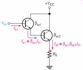
FIG. 28 A Darlington pair multiplies βac.
An Application
The emitter-follower is often used as an interface between a circuit with a high output resistance and a low-resistance load. In such an application, the emitter follower is called a buffer.
Suppose a common-emitter amplifier with a 1.0 k-Ω collector resistance must drive a low-resistance load such as an 8-Ω low-power speaker. If the speaker is capacitively coupled to the output of the amplifier, the 8-Ω load appears-to the ac signal-in parallel with the 1.0 k-Ω collector resistor. This results in an ac collector resistance of

…with an 8-Ω speaker load.
An emitter-follower using a Darlington pair can be used to interface the amplifier and the speaker, as shown in FIG. 29.
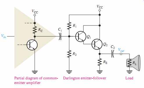
FIG. 29 A Darlington emitter-follower used as a buffer between a common
emitter amplifier and a low resistance load such as a speaker.
HISTORY NOTE
George Clifford Sziklai, born in Hungary in 1909, was an electronics engineer, who emigrated to New York in 1930. Among many other contributions to radio and TV, he invented the transistor configuration named after him, the Sziklai pair, also known as the complementary Darlington. Sziklai is also credited with constructing the first image orthicon television camera and inventing a high-speed elevator in addition to some 200 other patents.
The Sziklai Pair
The Sziklai pair, shown in FIG. 30, is similar to the Darlington pair except that it consists of two types of transistors, an npn and a pnp. This configuration is sometimes known as a complementary Darlington or a compound transistor. The current gain is about the same as in the Darlington pair, as illustrated. The difference is that the Q2 base current is the Q1 collector current instead of emitter current, as in the Darlington arrangement.
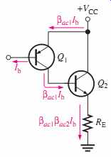
FIG. 30 The Sziklai pair.
An advantage of the Sziklai pair, compared to the Darlington, is that it takes less voltage to turn it on because only one barrier potential has to be overcome. A Sziklai pair is sometimes used in conjunction with a Darlington pair as the output stage of power amplifiers. In this case, the output power transistors are both the same type (two npn or two pnp transistors). This makes it easier to obtain exact matches of the output transistors, resulting in improved thermal stability and better sound quality in audio applications.
SECTION 4 CHECKUP
1. What is a common-collector amplifier called?
2. What is the ideal maximum voltage gain of a common-collector amplifier?
3. What characteristic of the common-collector amplifier makes it a useful circuit?
5. THE COMMON-BASE AMPLIFIER
The common-base (CB) amplifier provides high voltage gain with a maximum current gain of 1. Since it has a low input resistance, the CB amplifier is the most appropriate type for certain applications where sources tend to have very low-resistance outputs.
After completing this section, you should be able to:
-- Describe and analyze the operation of common-base amplifiers
-- Determine the voltage gain
-- Explain why there is no phase inversion
-- Discuss and calculate input resistance
-- Determine output resistance
-- Determine current gain
-- Determine power gain
FYI
The CB amplifier is useful at high frequencies when impedance matching is required because input impedance can be controlled and because noninverting amps have better frequency response.
A typical common-base amplifier is shown in FIG. 31. The base is the common terminal and is at ac ground because of capacitor C2. The input signal is capacitively coupled to the emitter. The output is capacitively coupled from the collector to a load resistor.
Voltage Gain
The voltage gain from emitter to collector is developed as follows (Vin = Ve, Vout = Vc).
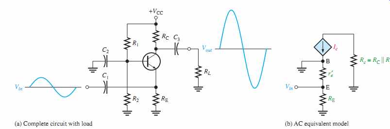
FIG. 31 Common-base amplifier with voltage-divider bias. (a) Complete
circuit with load (b) AC equivalent model

EQN. 18
where Rc = RC || RL. Notice that the gain expression is the same as for the common-emitter amplifier. However, there is no phase inversion from emitter to collector.
Input Resistance The resistance, looking in at the emitter, is:
EQN. 19
RE is typically much greater than r’e so the assumption that r’e || RE = r’e is usually valid.
The input resistance can be set to a desired value by using a swamping resistor.
Output Resistance
Looking into the collector, the ac collector resistance r’c, appears in parallel with RC. As you have previously seen in connection with the CE amplifier, r’c is typically much larger than RC, so a good approximation for the output resistance is
EQN. 20
Rout =RC
Current Gain
The current gain is the output current divided by the input current. Ic is the ac output cur rent, and Ie is the ac input current. Since the current gain is approximately 1. Ic = Ie,

EQN. 21
Power Gain
Since the current gain is approximately 1 for the common-base amplifier and Ap = Av Ai the power gain is approximately equal to the voltage gain.

EQN. 22
SECTION 5 CHECKUP
1. Can the same voltage gain be achieved with a common-base as with a common emitter amplifier?
2. Does the common-base amplifier have a low or a high input resistance?
3. What is the maximum current gain in a common-base amplifier?
6. MULTISTAGE AMPLIFIERS
Two or more amplifiers can be connected in a cascaded arrangement with the output of one amplifier driving the input of the next. Each amplifier in a cascaded arrangement is known as a stage. The basic purpose of a multistage arrangement is to increase the overall voltage gain. Although discrete multistage amplifiers are not as common as they once were, a familiarization with this area provides insight into how circuits affect each other when they are connected together.
After completing this section, you should be able to:
-- Describe and analyze the operation of multistage amplifiers
-- Determine the overall voltage gain of multistage amplifiers
-- Express the voltage gain in decibels (dB)
-- Discuss and analyze capacitively-coupled multistage amplifiers
-- Describe loading effects
-Determine the voltage gain of each stage in a two-stage amplifier
- Determine the overall voltage gain
- Determine the dc voltages
-- Describe direct-coupled multistage amplifiers
Multistage Voltage Gain
The overall voltage gain, A’v, of cascaded amplifiers, as shown in FIG. 33, is the product of the individual voltage gains.
EQN. 23
A’v = Av1 Av2 Av3 …Avn
where n is the number of stages.
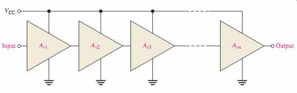
FIG. 33 Cascaded amplifiers. Each triangular symbol represents a separate
amplifier.
Amplifier voltage gain is often expressed in decibels (dB) as follows:
EQN. 24
Av(dB) = 20 log Av
This is particularly useful in multistage systems because the overall voltage gain in dB is the sum of the individual voltage gains in dB.
A’v(dB) = Av1(dB) + Av2(dB) + … + Avn(dB)
Capacitively-Coupled Multistage Amplifier
For purposes of illustration, we will use the two-stage capacitively coupled amplifier in FIG. 34. Notice that both stages are identical common-emitter amplifiers with the output of the first stage capacitively coupled to the input of the second stage. Capacitive coupling prevents the dc bias of one stage from affecting that of the other but allows the ac signal to pass without attenuation because XC = 0 Ω at the frequency of operation.
Notice, also, that the transistors are labeled Q1 and Q2.
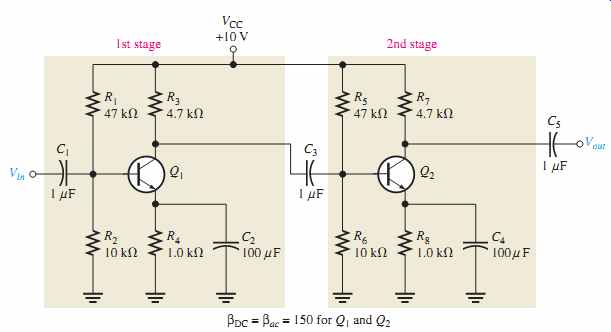
FIG. 34 A two-stage common-emitter amplifier.
Loading Effects
In determining the voltage gain of the first stage, you must consider the loading effect of the second stage. Because the coupling capacitor C3 effectively appears as a short at the signal frequency, the total input resistance of the second stage presents an ac load to the first stage.
Looking from the collector of Q1, the two biasing resistors in the second stage, R5 and R6, appear in parallel with the input resistance at the base of Q2. In other words, the signal at the collector of Q1 "sees" R3, R5, R6, and Rin(base2) of the second stage all in parallel to ac ground. Thus, the effective ac collector resistance of Q1 is the total of all these resistances in parallel, as FIG. 35 illustrates. The voltage gain of the first stage is reduced by the loading of the second stage because the effective ac collector resistance of the first stage is less than the actual value of its collector resistor, R3.
Remember that Av = Rc/r’e.
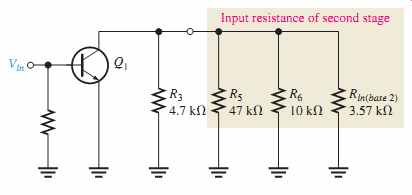
FIG. 35 AC equivalent of first stage in FIG. 34, showing loading from
second stage input resistance.
Voltage Gain of the First Stage
The ac collector resistance of the first stage is:
Rc1 = R3 || R5 || R6 || Rin(base2)
Remember that lowercase italic subscripts denote ac quantities such as for Rc.
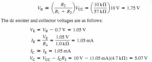
You can verify that IE = 1.05 mA, , and
The effective ac collector resistance of the first stage is as follows:
Rin(base2) = 3.57 k Ω. r’ e = 23.8 Ω =
Therefore, the base-to-collector voltage gain of the first stage is
Voltage Gain of the Second Stage
The second stage has no load resistor, so the ac collector resistance is R7, and the gain is
Compare this to the gain of the first stage, and notice how much the loading from the second stage reduced the gain.
Overall Voltage Gain
The overall amplifier gain with no load on the output is
A’v = Av1Av2 = (68.5)(197) = 13,495
If an input signal of , for example, is applied to the first stage and if there is no attenuation in the input base circuit due to the source resistance, an output from the second stage of will result. The overall voltage gain can be expressed in dB as follows:
(100 mV)(13,495) _ 1.35 V 100 mV
A’ v(dB) = 20 log (13,495) = 82.6 dB
DC Voltages in the Capacitively Coupled Multistage Amplifier
Since both stages in FIG. 34 are identical, the dc voltages for Q1 and Q2 are the same. Since and the dc base voltage for Q and Q is b R W R , bDCR4 W R2
Direct-Coupled Multistage Amplifiers
A basic two-stage, direct-coupled amplifier is shown in FIG. 36. Notice that there are no coupling or bypass capacitors in this circuit. The dc collector voltage of the first stage provides the base-bias voltage for the second stage. Because of the direct coupling, this type of amplifier has a better low-frequency response than the capacitively coupled type in which the reactance of coupling and bypass capacitors at very low frequencies may be come excessive. The increased reactance of capacitors at lower frequencies produces gain reduction in capacitively coupled amplifiers.
Direct-coupled amplifiers can be used to amplify low frequencies all the way down to dc (0 Hz) without loss of voltage gain because there are no capacitive reactances in the circuit.
The disadvantage of direct-coupled amplifiers, on the other hand, is that small changes in the dc bias voltages from temperature effects or power-supply variation are amplified by the succeeding stages, which can result in a significant drift in the dc levels throughout the circuit.
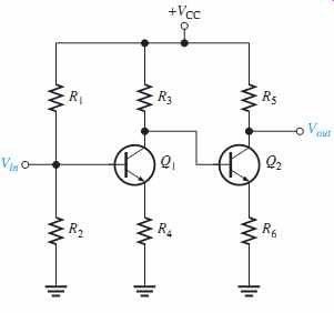
FIG. 36 A basic two-stage direct-coupled amplifier.
SECTION 6 CHECKUP
1. What does the term stage mean?
2. How is the overall voltage gain of a multistage amplifier determined?
3. Express a voltage gain of 500 in dB.
4. Discuss a disadvantage of a capacitively coupled amplifier.
7. THE DIFFERENTIAL AMPLIFIER
A differential amplifier is an amplifier that produces outputs that are a function of the difference between two input voltages. The differential amplifier has two basic modes of operation: differential (in which the two inputs are different) and common mode (in which the two inputs are the same). The differential amplifier is important in operational amplifiers, which are covered beginning in Section 12.
After completing this section, you should be able to:
-- Describe the differential amplifier and its operation
-- Discuss the basic operation
-- Calculate dc currents and voltages
-- Discuss the modes of signal operation
-- Describe single-ended differential input operation
- Describe double-ended differential input operation
- Determine common-mode operation
-- Define and determine the common-mode rejection ratio (CMRR)
Basic Operation
A basic differential amplifier (diff-amp) circuit is shown in FIG. 37. Notice that the differential amplifier has two inputs and two outputs.
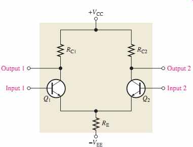
FIG. 37 Basic differential amplifier.
The following discussion is in relation to FIG. 38 and consists of a basic dc analysis of the diff-amp's operation. First, when both inputs are grounded (0 V), the emitters are at -0.7 V, as indicated in FIG. 38(a). It is assumed that the transistors are identically matched by careful process control during manufacturing so that their dc emitter currents are the same when there is no input signal. Thus,

This condition is illustrated in FIG. 38(a).
Next, input 2 is left grounded, and a positive bias voltage is applied to input 1, as shown in FIG. 38(b). The positive voltage on the base of Q1 increases IC1 and raises the emitter voltage to
VE = VB - 0.7 V
This action reduces the forward bias (VBE) of Q2 because its base is held at 0 V (ground), thus causing IC2 to decrease. The net result is that the increase in IC1 causes a decrease in VC1, and the decrease in IC2 causes an increase in VC2, as shown.
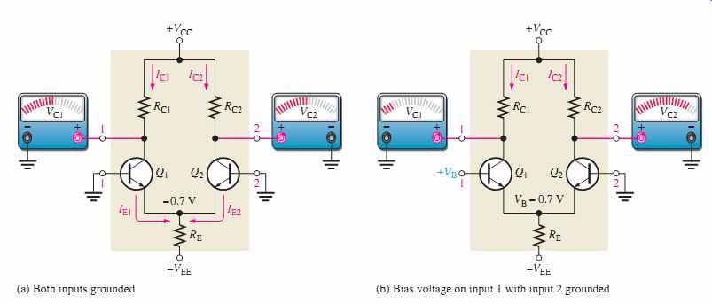
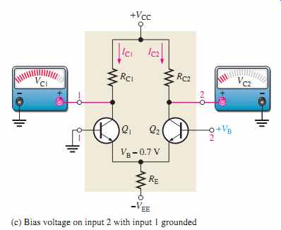
FIG. 38 Basic operation of a differential amplifier (ground is zero volts)
showing relative changes in voltages.(a) Both inputs grounded (b) Bias
voltage on input 1 with input 2 grounded (c) Bias voltage on input 2 with
input 1 grounded.
Finally, input 1 is grounded and a positive bias voltage is applied to input 2, as shown in FIG. 38(c). The positive bias voltage causes Q2 to conduct more, thus increasing IC2.
Also, the emitter voltage is raised. This reduces the forward bias of Q1, since its base is held at ground, and causes IC1 to decrease. The result is that the increase in IC2 produces a decrease in VC2, and the decrease in IC1 causes VC1 to increase, as shown.
Modes of Signal Operation
Single-Ended Differential Input
When a diff-amp is operated with this input configuration, one input is grounded and the signal voltage is applied only to the other input, as shown in FIG. 39. In the case where the signal voltage is applied to input 1 as in part (a), an inverted, amplified signal voltage appears at output 1 as shown. Also, a signal volt age appears in phase at the emitter of Q1. Since the emitters of Q1 and Q2 are common, the emitter signal becomes an input to Q2, which functions as a common-base amplifier. The signal is amplified by Q2 and appears, non-inverted, at output 2. This action is illustrated in part (a).
In the case where the signal is applied to input 2 with input 1 grounded, as in FIG. 39(b), an inverted, amplified signal voltage appears at output 2. In this situation, Q1 acts as a common-base amplifier, and a non-inverted, amplified signal appears at output 1.
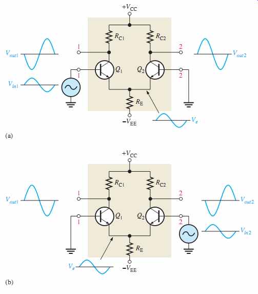
FIG. 39 Single-ended differential input operation.
Double-Ended Differential Inputs
In this input configuration, two opposite-polarity (out-of-phase) signals are applied to the inputs, as shown in FIG. 40(a). Each input affects the outputs, as you will see in the following discussion.
FIG. 40(b) shows the output signals due to the signal on input 1 acting alone as a single-ended input. FIG. 40(c) on page 308 shows the output signals due to the signal on input 2 acting alone as a single-ended input. Notice in parts (b) and (c) that the signals on output 1 are of the same polarity. The same is also true for output 2. By superimposing both output 1 signals and both output 2 signals, you get the total output signals, as shown in FIG. 40(d).
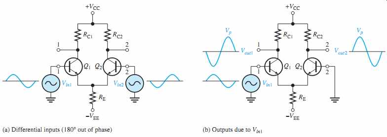
FIG. 40 Double-ended differential operation. (continued on next page)
(a) Differential inputs (180° out of phase) (b) Outputs due to Vin1
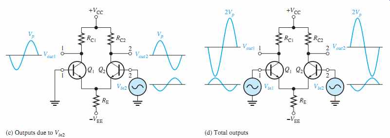
FIG. 40 (c) Outputs due to V (d) Total outputs
Common-Mode Inputs
One of the most important aspects of the operation of a diff amp can be seen by considering the common-mode condition where two signal voltages of the same phase, frequency, and amplitude are applied to the two inputs, as shown in FIG. 41(a). Again, by considering each input signal as acting alone, you can under stand the basic operation.
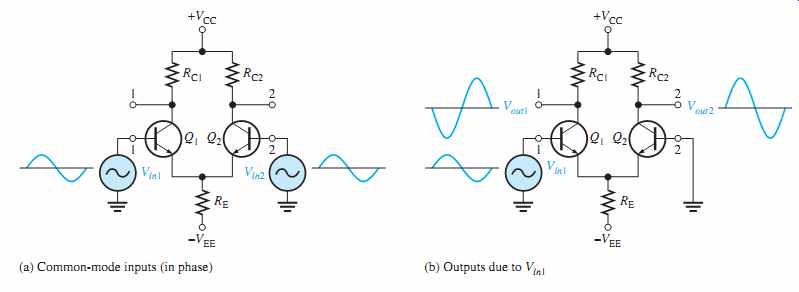
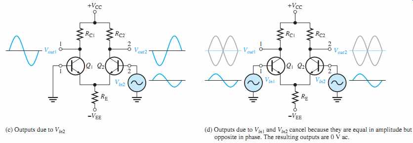
FIG. 41 Common-mode operation of a differential amplifier.
(a) Common-mode inputs (in phase) (b) Outputs due to Vin1 (c) Outputs due to Vin2 (d) Outputs due to Vin1 and Vin2 cancel because they are equal in amplitude but opposite in phase. The resulting outputs are 0 V ac.
FIG. 41(b) shows the output signals due to the signal on only input 1, and FIG. 41(c) shows the output signals due to the signal on only input 2. Notice that the corresponding signals on output 1 are of the opposite polarity, and so are the ones on output 2.
When the input signals are applied to both inputs, the outputs are superimposed and they cancel, resulting in a zero output voltage, as shown in FIG. 41(d).
This action is called common-mode rejection. Its importance lies in the situation where an unwanted signal appears commonly on both diff-amp inputs. Common-mode rejection means that this unwanted signal will not appear on the outputs and distort the desired signal. Common-mode signals (noise) generally are the result of the pick-up of radiated energy on the input lines from adjacent lines, the 60 Hz power line, or other sources.
Common-Mode Rejection Ratio
Desired signals appear on only one input or with opposite polarities on both input lines.
These desired signals are amplified and appear on the outputs as previously discussed.
Unwanted signals (noise) appearing with the same polarity on both input lines are essentially cancelled by the diff-amp and do not appear on the outputs. The measure of an amplifier's ability to reject common-mode signals is a parameter called the CMRR (common mode rejection ratio).
Ideally, a diff-amp provides a very high gain for desired signals (single-ended or differential) and zero gain for common-mode signals. Practical diff-amps, however, do exhibit a very small common-mode gain (usually much less than 1), while providing a high differential voltage gain (usually several thousand). The higher the differential gain with respect to the common-mode gain, the better the performance of the diff-amp in terms of rejection of common-mode signals. This suggests that a good measure of the diff-amp's performance in rejecting unwanted common-mode signals is the ratio of the differential voltage gain Av(d ) to the common-mode gain, Acm. This ratio is the common-mode rejection ratio, CMRR.
EQN. 25
CMRR= Av(d ) / Acm
The higher the CMRR, the better. A very high value of CMRR means that the differential gain Av(d) is high and the common-mode gain Acm is low.
The CMRR is often expressed in decibels (dB) as
EQN. 26
CMRR = 20 log (Av(d ) / Acm)
A CMRR of 10,000 means that the desired input signal (differential) is amplified 10,000 times more than the unwanted noise (common-mode). For example, if the amplitudes of the differential input signal and the common-mode noise are equal, the desired signal will appear on the output 10,000 times greater in amplitude than the noise. Thus, the noise or interference has been essentially eliminated.
SECTION 7 CHECKUP
1. Distinguish between double-ended and single-ended differential inputs.
2. Define common-mode rejection.
3. For a given value of differential gain, does a higher CMRR result in a higher or lower common-mode gain?
8. TROUBLESHOOTING
In working with any circuit, you must first know how it is supposed to work before you can troubleshoot it for a failure. The two-stage capacitively coupled amplifier discussed in SECTION 6 is used to illustrate a typical troubleshooting procedure.
After completing this section, you should be able to:
-- Troubleshoot amplifier circuits
-- Discuss a troubleshooting procedure
-- Describe the analysis phase
-Describe the planning phase
-Describe the measurement phase
When you are faced with having to troubleshoot a circuit, the first thing you need is a schematic with the proper dc and signal voltages labeled. You must know what the correct voltages in the circuit should be before you can identify an incorrect voltage. Schematics of some circuits are available with voltages indicated at certain points. If this is not the case, you must use your knowledge of the circuit operation to determine the correct volt ages. FIG. 42 is the schematic for the two-stage amplifier that was analyzed in SECTION 6. The correct voltages are indicated at each point.
Troubleshooting Procedure
The analysis, planning, and measurement approach to troubleshooting, discussed in Section 2, will be used.
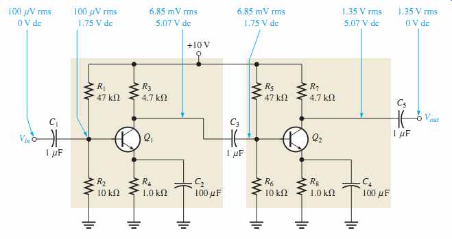
FIG. 42 A two-stage common-emitter amplifier with correct voltages indicated.
Both transistors have dc and ac betas of 150. Different values of Beta
will produce slightly different results.
Analysis
It has been found that there is no output voltage, Vout. You have also deter mined that the circuit did work properly and then failed. A visual check of the circuit board or assembly for obvious problems such as broken or poor connections, solder splashes, wire clippings, or burned components turns up nothing. You conclude that the problem is most likely a faulty component in the amplifier circuit or an open connection. Also, the dc supply voltage may not be correct or may be missing.
Planning
You decide to use an oscilloscope to check the dc levels and the ac signals (you prefer to use a DMM to measure the dc voltages) at certain test points. Also, you decide to apply the half-splitting method to trace the voltages in the circuit and use an in-circuit transistor tester if a transistor is suspected of being faulty.
Measurement
To determine the faulty component in a multistage amplifier, use the general five-step troubleshooting procedure which is illustrated as follows.
Step 1: Perform a power check. Assume the dc supply voltage is correct as indicated in FIG. 43.
Step 2: Check the input and output voltages. Assume the measurements indicate that the input signal voltage is correct. However, there is no output signal voltage or the output signal voltage is much less than it should be, as shown by the diagram in FIG. 43.
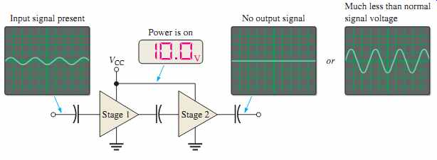
FIG. 43 Initial check of a faulty two-stage amplifier.
Step 3: Apply the half-splitting method of signal tracing. Check the voltages at the output of the first stage. No signal voltage or a much less than normal signal voltage indicates that the problem is in the first stage. An incorrect dc volt age also indicates a first-stage problem. If the signal voltage and the dc voltage are correct at the output of the first stage, the problem is in the second stage. After this check, you have narrowed the problem to one of the two stages. This step is illustrated in FIG. 44.
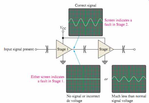
FIG. 44 Half-splitting signal tracing isolates the faulty stage.
Step 4: Apply fault analysis. Focus on the faulty stage and determine the component failure that can produce the incorrect output.
Symptom: DC voltages incorrect.
Likely faults: A failure of any resistor or the transistor will produce an incorrect dc bias voltage. A leaky bypass or coupling capacitor will also affect the dc bias voltages. Further measurements in the stage are necessary to isolate the faulty component.
Incorrect ac voltages and the most likely fault(s) are illustrated in FIG. 45 as follows:
(a) Symptom 1: Signal voltage at output missing; dc voltage correct.
Symptom 2: Signal voltage at base missing; dc voltage correct.
Likely fault: Input coupling capacitor open. This prevents the signal from getting to the base.
(b) Symptom: Correct signal at base but no output signal.
Likely fault: Transistor base open.
(c) Symptom: Signal voltage at output much less than normal; dc voltage correct.
Likely fault: Bypass capacitor open.
Step 5: Replace or repair. With the power turned off, replace the defective component or repair the defective connection. Turn on the power, and check for proper operation.
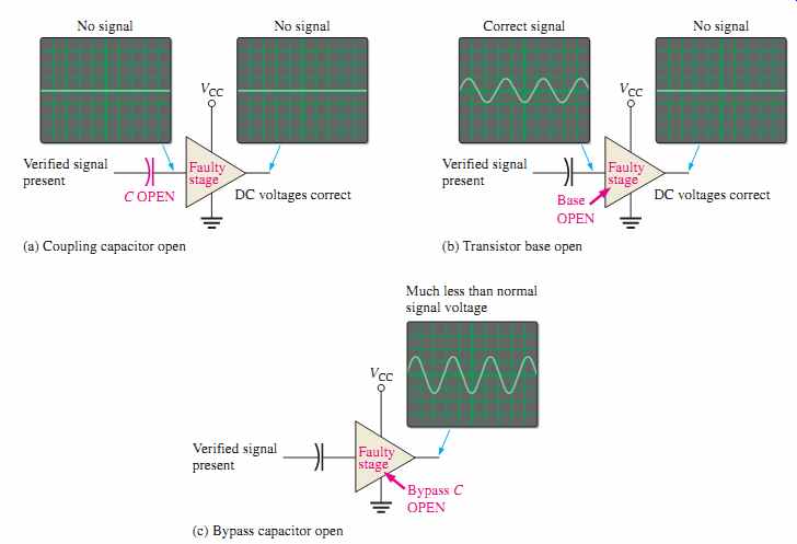
FIG. 45 Troubleshooting a faulty stage. (a) Coupling capacitor open (b)
Transistor base open (c) Bypass capacitor open
SECTION 8 CHECKUP
1. If C4 in FIG. 42 were open, how would the output signal be affected? How would the dc level at the collector of Q2 be affected?
2. If R5 in FIG. 42 were open, how would the output signal be affected?
3. If the coupling capacitor C3 in FIG. 42 shorted out, would any of the dc voltages in the amplifier be changed? If so, which ones?