AMAZON multi-meters discounts AMAZON oscilloscope discounts
<< cont. from part 2
Application Activity: Audio Preamplifier for PA System
An audio preamplifier is to be developed for use in a small portable public address (PA) system. The preamplifier will have a microphone input, and its output will drive a power amplifier to be developed in Section 7. A block diagram of the complete PA system is shown in FIG. 46(a), and its physical configuration is shown in part (b). The dc supply voltages are provided by a battery pack or by an electronic power supply.
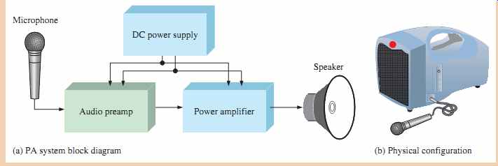
FIG. 46 The public address system.
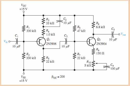
FIG. 47 Two-stage voltage preamplifier.
The Circuit
A 2-stage audio voltage preamplifier is shown in FIG. 47. The first stage is a common emitter pnp with voltage-divider bias, and the second stage is a common-emitter npn with voltage-divider bias. It has been decided that the amplifier should operate from 30 V dc to get a large enough signal voltage swing to provide a maximum of 6 W to the speaker.
Because small IC regulators such as the 78xx and 79xx series are not available above 24 V, dual +/- 15 V dc supplies are used in this particular system instead of a single supply.
The operation is essentially the same as if a single +30 V dc source had been used. The potentiometer at the output provides gain adjustment for volume control. The input to the first stage is from the microphone, and the output of the second stage will drive a power amplifier to be developed in Section 7. The power amplifier will drive the speaker. The preamp is to operate with a peak input signal range of from 25 mV to 50 mV. The minimum range of voltage gain adjustment is from 90 to 170.
1. Calculate the theoretical voltage gain of the first stage when the second stage is set for maximum gain.
2. Calculate the theoretical maximum voltage gain of the second stage.
3. Determine the overall theoretical voltage gain.
4. Calculate the circuit power dissipation with no signal (quiescent).
Simulation
The preamp is simulated with a peak input signal of 45 mV using Multisim. The results are shown in FIG. 48.
5. Determine the voltage gain of the simulated circuit based on the voltage measurements.
6. Compare the measured voltage gain with the calculated voltage gain.

FIG. 48 Preamp input and output signals. (a) Circuit screen (b) Input
signal (yellow) and output signal (blue)
Prototyping and Testing*
Now that the circuit has been simulated, the prototype circuit is constructed and tested.
After the circuit is successfully tested on a protoboard, it is ready to be finalized on a printed circuit board.
Circuit Board
The preamp is implemented on a printed circuit board as shown in FIG. 49.
7. Check the printed circuit board and verify that it agrees with the schematic in FIG. 47. The volume control potentiometer is mounted off the PC board for easy access.
8. Label each input and output pin according to function.
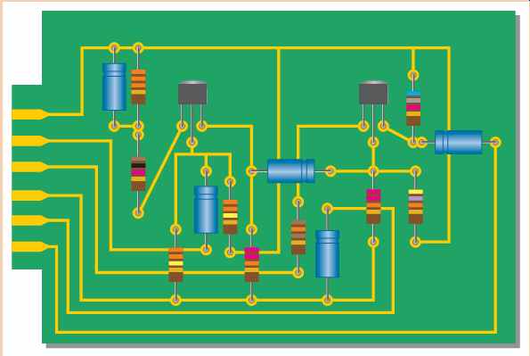
FIG. 49 Preamp circuit board.
Troubleshooting
Two preamp circuit boards have failed the production test. You will troubleshoot the boards based on the scope measurements shown in FIG. 50.
9. List possible faults for board 1.
10. List possible faults for board 2.
FIG. 50 Test of two faulty preamp boards.
---------------
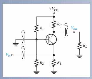
SUMMARY OF THE COMMON-EMITTER AMPLIFIER
CIRCUIT WITH VOLTAGE-DIVIDER BIAS
¦ Input is at the base. Output is at the collector.
¦ There is a phase inversion from input to output.
¦ C1 and C3 are coupling capacitors for the input and output signals.
¦ C2 is the emitter-bypass capacitor.
¦ All capacitors must have a negligible reactance at the frequency of operation, so they appear as shorts.
¦ Emitter is at ac ground due to the bypass capacitor.
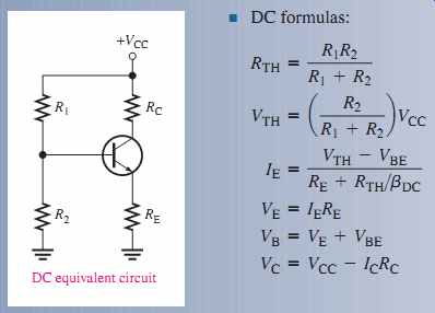
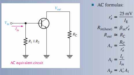
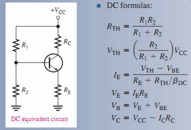
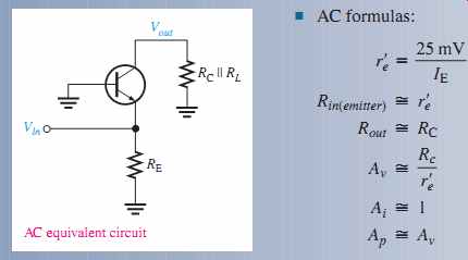
EQUIVALENT CIRCUITS AND FORMULAS
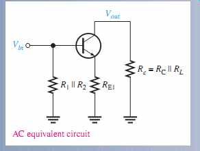
SWAMPED AMPLIFIER WITH RESISTIVE LOAD
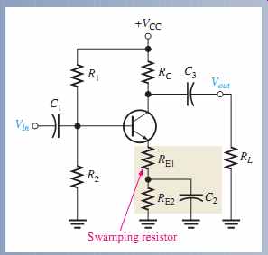
¦ Swamping stabilizes gain by minimizing the effect of r’ e.
¦ Swamping reduces the voltage gain from its unswamped value.
¦ Swamping increases input resistance.
¦ The load resistance reduces the voltage gain. The smaller the load resistance, the less the gain.
-----------------------
------------------------
SUMMARY OF COMMON-BASE AMPLIFIER
CIRCUIT WITH VOLTAGE-DIVIDER BIAS
¦ Input is at the emitter. Output is at the collector.
¦ There is no phase inversion from input to output.
¦ Input resistance is low. Output resistance is high.
¦ Maximum current gain is 1.
¦ Base is at ac ground.
EQUIVALENT CIRCUITS AND FORMULAS
-----------------------------
----------------------------
SUMMARY OF DIFFERENTIAL AMPLIFIER
CIRCUIT WITH DIFFERENTIAL INPUTS
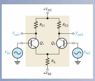
¦ Double-ended differential inputs (shown) Signal on both inputs Input signals are out of phase
¦ Single-ended differential inputs (not shown) Signal on one input only One input connected to ground
CIRCUIT WITH COMMON-MODE INPUTS
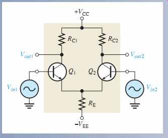
¦ Both input signals are the same phase, frequency, and amplitude.
¦ Common-mode rejection ratio:
---------------------------------
SUMMARY
SECTION 1
-- A small-signal amplifier uses only a small portion of its load line under signal conditions.
-- The ac load line differs from the dc load line because the effective ac collector resistance is less than the dc collector resistance.
SECTION 2
-- r parameters are easily identifiable and applicable with a transistor's circuit operation.
-- h parameters are important because manufacturers' datasheets specify transistors using h parameters.
SECTION 3
-- A common-emitter amplifier has high voltage, current, and power gains, but a relatively low input resistance.
-- Swamping is a method of stabilizing the voltage gain.
SECTION 4
-- A common-collector amplifier has high input resistance and high current gain, but its voltage gain is approximately 1.
-- A Darlington pair provides beta multiplication for increased input resistance.
-- A common-collector amplifier is known as an emitter-follower.
SECTION 5
-- The common-base amplifier has a high voltage gain, but it has a very low input resistance and its current gain is approximately 1.
-- Common-emitter, common-collector, and common-base amplifier configurations are summarized in TABLE 4.
SECTION 6
-- The total gain of a multistage amplifier is the product of the individual gains (sum of dB gains).
-- Single-stage amplifiers can be connected in sequence with capacitively-coupling and direct coupling methods to form multistage amplifiers.
SECTION 7
-- A differential input voltage appears between the inverting and noninverting inputs of a differential amplifier.
-- In the differential mode, a diff-amp can be operated with single-ended or double-ended inputs.
-- In single-ended operation, there is a signal on one input and the other input is grounded.
-- In double-ended operation, two signals that are 180° out of phase are on the inputs.
-- Common-mode occurs when equal in-phase voltages are applied to both input terminals.
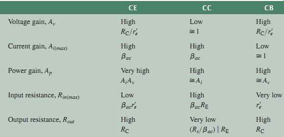
TABLE 4 Relative comparison of amplifier configurations. The current gains
and the input and output resistances are the approximate maximum achievable
values, with the bias resistors neglected.
TERMS
ac ground--A point in a circuit that appears as ground to ac signals only.
Attenuation--The reduction in the level of power, current, or voltage.
Bypass capacitor--A capacitor placed across the emitter resistor of an amplifier.
CMRR (common-mode rejection ratio)--A measure of a differential amplifier's ability to reject common-mode signals.
Common-base (CB)--A BJT amplifier configuration in which the base is the common terminal to an ac signal or ground.
Common-collector (CC)--A BJT amplifier configuration in which the collector is the common terminal to an ac signal or ground.
Common-emitter (CE)--A BJT amplifier configuration in which the emitter is the common terminal to an ac signal or ground.
Common mode--A condition where two signals applied to differential inputs are of the same phase, frequency, and amplitude.
Decibel--A logarithmic measure of the ratio of one voltage to another or one power to another.
Differential amplifier--An amplifier in which the output is a function of the difference between two input voltages.
Emitter-follower--A popular term for a common-collector amplifier.
Input resistance--The resistance seen by an ac source connected to the input of an amplifier.
Output resistance--The ac resistance looking in at the output of an amplifier.
r parameter--One of a set of BJT characteristic parameters that include αac, βac, r’ e, r’ b, and r’ c.
FORMULAS
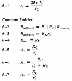
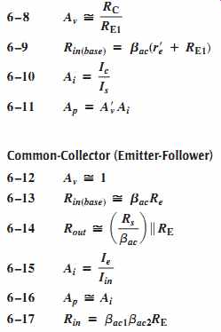
Internal ac emitter resistance Total amplifier input resistance, voltage-divider bias Input resistance at base Output resistance Voltage gain, base-to-collector, unloaded Voltage gain without bypass capacitor Voltage gain, base-to-collector, loaded, bypassed RE
Voltage gain, swamped amplifier Input resistance at base, swamped amplifier Current gain, input source to collector Power gain Voltage gain, base-to-emitter Input resistance at base, loaded Output resistance Current gain Power gain Input resistance, Darlington pair Voltage gain, emitter-to-collector Input resistance at emitter Output resistance Current gain Power gain Overall voltage gain Voltage gain expressed in dB Common-mode rejection ratio Common mode rejection ratio in dB
TRUE/FALSE QUIZ
1. In an amplifier, a coupling capacitor should appear ideally as a short to the signal.
2. r parameters include βac and r’ e.
3. h parameters are never specified on a datasheet.
4. The r parameter βac is the same as the h parameter hfe.
5. A bypass capacitor in a CE amplifier decreases the voltage gain.
6. If RC in a CE amplifier is increased, the voltage gain is reduced.
7. The load is the amount of current drawn from the output of an amplifier.
8. In a CE amplifier, the gain can be stabilized by using a swamping resistor.
9. An emitter-follower is a CC amplifier.
10. A CC amplifier has high voltage gain.
11. A Darlington pair consists essentially of two CC amplifiers.
12. A CB amplifier has high current gain.
13. The overall voltage gain of a multistage amplifier is the product of the gains of each stage.
14. A differential amplifier amplifies the difference of two input signals.
15. CMRR is the common-mode resistance ratio.
CIRCUIT-ACTION
1. If the transistor in FIG. 8 is exchanged for one with higher betas, Vout will (a) increase (b) decrease (c) not change
2. If C2 is removed from the circuit in FIG. 8, Vout will (a) increase (b) decrease (c) not change
3. If the value of RC in FIG. 8 is increased, Vout will (a) increase (b) decrease (c) not change
4. If the amplitude of Vin in FIG. 8 is decreased, Vout will (a) increase (b) decrease (c) not change
5. If C2 in FIG. 27 is shorted, the average value of the output voltage will (a) increase (b) decrease (c) not change
6. If the value of RE in FIG. 27 is increased, the voltage gain will (a) increase (b) decrease (c) not change
7. If the value of C1 in FIG. 27 is increased, Vout will (a) increase (b) decrease (c) not change
8. If the value of RC in FIG. 32 is increased, the current gain will (a) increase (b) decrease (c) not change
9. If C2 and C4 in FIG. 34 are increased in value, Vout will (a) increase (b) decrease (c) not change
10. If the value of R4 in FIG. 34 is reduced, the overall voltage gain will (a) increase (b) decrease (c) not change
SELF-TEST
SECTION 1
1. A small-signal amplifier (a) uses only a small portion of its load line (b) always has an output signal in the mV range (c) goes into saturation once on each input cycle (d) is always a common-emitter amplifier
SECTION 2
2. The parameter hfe corresponds to (a) βDC (b) βac (c) r’e (d) r’c
3. If the dc emitter current in a certain transistor amplifier is 3 mA, the approximate value of r’e is (a) 3-kΩ (b) 3-Ω (c) 8.33-Ω (d) 0.33 k-Ω
SECTION 3
4. A certain common-emitter amplifier has a voltage gain of 100. If the emitter bypass capacitor is removed, (a) the circuit will become unstable (b) the voltage gain will decrease (c) the voltage gain will increase (d) the Q-point will shift
5. For a common-emitter amplifier, RC = 1.0 k Ω, RE = 390 Ω, r’e = 15-Ω, and βac = 75.
Assuming that RE is completely bypassed at the operating frequency, the voltage gain is (a) 66.7 (b) 2.56 (c) 2.47 (d) 75
6. In the circuit of Question 5, if the frequency is reduced to the point where XC(bypass)=RE, the voltage gain (a) remains the same (b) is less (c) is greater
7. In a common-emitter amplifier with voltage-divider bias, Rin(base) = 68 k Ω, R1 = 33 k Ω,
R2 = 15 k Ω.
The total ac input resistance is:
(a) (b) (c) (d)
8. A CE amplifier is driving a load. If the voltage gain is approximately (a) 220 (b) 1000 (c) 10 (d) 180
SECTION 4
9. For a common-collector amplifier, The ac input resistance at the base is (a) (b) (c) (d)
10. If a 10 mV signal is applied to the base of the emitter-follower circuit in Question 9, the output signal is approximately (a) 100 mV (b) 150 mV (c) 1.5 V (d) 10 mV
11. In a certain emitter-follower circuit, the current gain is 50. The power gain is approximately (a) 50Av (b) 50 (c) 1 (d) answers (a) and (b)
12. In a Darlington pair configuration, each transistor has an ac beta of 125. If RE is the input resistance is (a) (b) (c) (d) SECTION 5
13. The input resistance of a common-base amplifier is (a) very low (b) very high (c) the same as a CE (d) the same as a CC SECTION 6
14. Each stage of a four-stage amplifier has a voltage gain of 15. The overall voltage gain is (a) 60 (b) 15 (c) 50,625 (d) 3078
15. The overall gain found in Question 14 can be expressed in decibels as (a) 94.1 dB (b) 47.0 dB (c) 35.6 dB (d) 69.8 dB SECTION 7
16. A differential amplifier (a) is used in op-amps (b) has one input and one output (c) has two outputs (d) answers (a) and (c)
17. When a differential amplifier is operated single-ended, (a) the output is grounded (b) one input is grounded and a signal is applied to the other (c) both inputs are connected together (d) the output is not inverted
18. In the double-ended differential mode, (a) opposite polarity signals are applied to the inputs (b) the gain is 1 (c) the outputs are different amplitudes (d) only one supply voltage is used
19. In the common mode, (a) both inputs are grounded (b) the outputs are connected together (c) an identical signal appears on both inputs (d) the output signals are in-phase
140 kΩ 8.75-M-Ω 70-kΩ 560-Ω 560-Ω, 16.5 kΩ 110-Ω 15-kΩ 1500-Ω RE = 100-Ω, r’e = 10-Ω, and βac = 150.
RC = 2.2 k Ω and r’ e = 10-Ω, 10 kΩ 12.3 kΩ 22.2 kΩ 8.95 kΩ 68 kΩ and =
PROBLEMS
BASIC PROBLEMS
SECTION 1
Amplifier Operation
1. What is the lowest value of dc collector current to which a transistor having the characteristic curves in FIG. 4 can be biased and still retain linear operation with a peak-to-peak base current swing of
2. What is the highest value of IC under the conditions described in Problem 1?
SECTION 2
Transistor AC Models
3. If the dc emitter current in a transistor is 3 mA, what is the value of
4. If the hfe of a transistor is specified as 200, determine
5. A certain transistor has a dc beta (hFE) of 130. If the dc base current is determine
6. At the dc bias point of a certain transistor circuit, Also, a variation in IB of about the Q-point produces a variation in IC of 0.35 mA about the Q-point.
Determine
SECTION 3
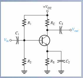
The Common-Emitter Amplifier
7. Draw the dc equivalent circuit and the ac equivalent circuit for the unloaded amplifier in FIG. 51.
8. Determine the following dc values for the amplifier in FIG. 51.
(a) VB (b) VE (c) IE (d) IC (e) VC
9. Calculate the quiescent power dissipation in FIG. 51.
10. Determine the following values for the amplifier in FIG. 51.
(a) Rin(base) (b) Rin(tot) (c) Av 11. Connect a bypass capacitor across RE in FIG. 51, and repeat Problem 10.
12. Connect a load resistor to the output in FIG. 51, and repeat Problem 11.
13. Determine the following dc values for the amplifier in FIG. 52.
(a) IE (b) VE (c) VB (d) IC (e) VC (f) VCE 10 k Ω βDC and βac.
3 mA IB = 15 mA and IC = 2 mA.
r’ e. αDC = 0.99.
10 mA, βac.
r’e? 20 mA?
14. Determine the following ac values for the amplifier in FIG. 52.
(a) Rin(base) (b) Rin (c) Av (d) Ai (e) Ap
15. Assume that a voltage source is driving the amplifier in FIG. 52.
Determine the overall voltage gain by taking into account the attenuation in the base circuit, and find the total output voltage (ac and dc). What is the phase relationship of the collector signal voltage to the base signal voltage?
16. The amplifier in FIG. 53 has a variable gain control, using a potentiometer for RE with the wiper ac-grounded. As the potentiometer is adjusted, more or less of RE is bypassed to ground, thus varying the gain. The total RE remains constant to dc, keeping the bias fixed.
Determine the maximum and minimum gains for this unloaded amplifier.
17. If a load resistance of is placed on the output of the amplifier in FIG. 53, what are the maximum and minimum gains?
18. Find the overall maximum voltage gain for the amplifier in FIG. 53 with a load if it is being driven by a source.
300 k 1.0 k-Ω 600 Ω 100 Ω 600 Ω, 12 mV rms
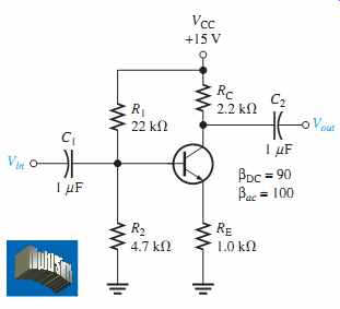
FIG. 51 Multisim file circuits are identified with a logo Filenames correspond
to figure numbers (e.g., FIG-51).
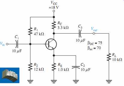
FIG. 52
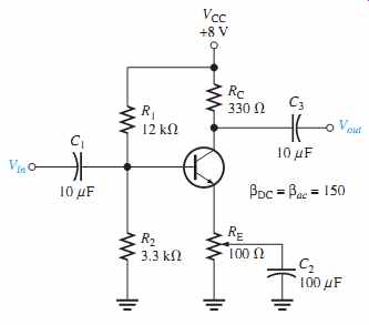
FIG. 53
19. Modify the schematic to show how you would "swamp out" the temperature effects of in FIG. 52 by making Re at least ten times larger than Keep the same total RE. How does this affect the voltage gain?
r’e.
r’e
SECTION 4
The Common-Collector Amplifier
20. Determine the exact voltage gain for the unloaded emitter-follower in FIG. 54.
21. What is the total input resistance in FIG. 54? What is the dc output voltage?
22. A load resistance is capacitively coupled to the emitter in FIG. 54. In terms of signal operation, the load appears in parallel with RE and reduces the effective emitter resistance.
How does this affect the voltage gain?
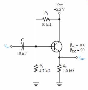
FIG. 54
23. In Problem 22, what value of RL will cause the voltage gain to drop to 0.9?
24. For the circuit in FIG. 55, determine the following:
(a) Q1 and Q2 dc terminal voltages (b) overall (c) for each transistor (d) total input resistance
25. Find the overall current gain A in FIG. 55.
r’ e bac
FIG. 55
SECTION 5
The Common-Base Amplifier
26. What is the main disadvantage of the common-base amplifier compared to the common-emitter and the emitter-follower amplifiers? 27. Find for the unloaded amplifier in FIG. 56.
28. Match the following generalized characteristics with the appropriate amplifier configuration.
(a) Unity current gain, high voltage gain, very low input resistance (b) High current gain, high voltage gain, low input resistance (c) High current gain, unity voltage gain, high input resistance Rin(emitter), Av, Ai, and Ap
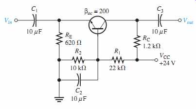
FIG. 56
SECTION 6
Multistage Amplifiers
29. Each of two cascaded amplifier stages has an
What is the overall gain?
30. Each of three cascaded amplifier stages has a dB voltage gain of 10 dB. What is the overall voltage gain in dB? What is the actual overall voltage gain? Av = 20.
31. For the two-stage, capacitively coupled amplifier in FIG. 57, find the following values:
(a) voltage gain of each stage (b) overall voltage gain (c) Express the gains found in (a) and (b) in dB.
32. If the multistage amplifier in FIG. 57 is driven by a source and the second stage is loaded with an determine (a) voltage gain of each stage (b) overall voltage gain (c) Express the gains found in (a) and (b) in dB.
RL = 18 k Ω, 75 Ω, 50 mV
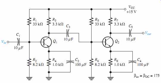
FIG. 57
33. FIG. 58 shows a direct-coupled (that is, with no coupling capacitors between stages)
two-stage amplifier. The dc bias of the first stage sets the dc bias of the second. Determine all dc voltages for both stages and the overall ac voltage gain.
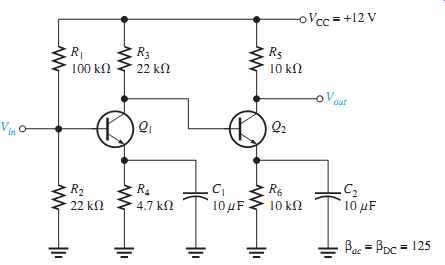
FIG. 58
34. Express the following voltage gains in dB: (a) 12 (b) 50 (c) 100 (d) 2500
35. Express the following voltage gains in dB as standard voltage gains:
(a) 3 dB (b) 6 dB (c) 10 dB (d) 20 dB (e) 40 dB
SECTION 7
The Differential Amplifier
36. The dc base voltages in FIG. 59 are zero. Using your knowledge of transistor analysis, determine the dc differential output voltage. Assume that Q1 has an and Q2 has an a = 0.975.
a = 0.980
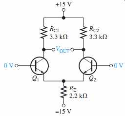
FIG. 59
37. Identify the quantity being measured by each meter in FIG. 60.
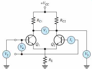
FIG. 60
38. A differential amplifier stage has collector resistors of each. If what is the differential output voltage?
39. Identify the type of input and output configuration for each basic differential amplifier in FIG. 61.
IC1 = 1.35 mA and IC2 = 1.29 mA, 5.1 k Ω
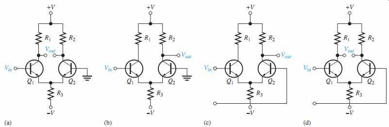
FIG. 61
SECTION 8
Troubleshooting
40. Assume that the coupling capacitor C3 is shorted in FIG. 34. What dc voltage will appear at the collector of Q1?
41. Assume that R5 opens in FIG. 34. Will Q2 be in cutoff or in conduction? What dc voltage will you observe at the Q2 collector?
42. Refer to FIG. 57 and determine the general effect of each of the following failures:
(a) C2 open (b) C3 open (c) C4 open (d) C2 shorted (e) base-collector junction of Q1 open (f ) base-emitter junction of Q2 open
43. Assume that you must troubleshoot the amplifier in FIG. 57. Set up a table of test point values, input, output, and all transistor terminals that include both dc and rms values that you expect to observe when a 300-Ω test signal source with a 25 uV rms output is used.
APPLICATION PROBLEMS
44. Refer to the public address system block diagram in FIG. 46. You are asked to repair a sys tem that is not working. After a preliminary check, you find that there is no output signal from the power amplifier or from the preamplifier. Based on this check and assuming that only one of the blocks is faulty, which block can you eliminate as the faulty one? What would you check next?
45. What effect would each of the following faults in the amplifier of FIG. 62 have on the out put signal? (a) Open C1 (b) Open C2 (c) Open C3 (d) Open C4 (e) Q1 collector internally open (f ) Q2 emitter shorted to ground
46. Suppose a 220-ohm resistor is incorrectly installed in the R7 position of the amplifier in Figure 62. What effect does this have on the circuit?
47. The connection from R1 to the supply voltage V1 in Figure 6–62 has opened.
(a) What happens to Q1?
(b) What is the dc voltage at the Q1 collector?
(c) What is the dc voltage at the Q2 collector?
DATASHEET PROBLEMS
48. Refer to the 2N3946/2N3947 partial datasheet in FIG. 63 on page 334. Determine the minimum value for each of the following r parameters:
(a) βac (b) r’c (c) r’e
49. Repeat Problem 48 for maximum values.
50. Should you use a 2N3946 or a 2N3947 transistor in a certain application if the criteria is maximum current gain?

FIG. 63 Partial datasheet for the 2N3946/2N3947.
ADVANCED PROBLEMS
51. In an amplifier such as the one in FIG. 62, explain the general effect that a leaky coupling capacitor would have on circuit performance.
52. Draw the dc and ac equivalent circuits for the amplifier in FIG. 62.
53. Modify the 2-stage amplifier in FIG. 62 to drive a load of 10-k Ω and maintain the same voltage gain.
54. Design a single-stage common-emitter amplifier with a voltage gain of 40 dB that operates from a dc supply voltage of +12 V. Use a 2N2222 transistor, voltage-divider bias, and a 330-Ω swamping resistor. The maximum input signal is 25 mV rms.
55. Design an emitter-follower with a minimum input resistance of 50-kΩ using a 2N3904 npn transistor with a βac = 100.
56. Repeat Problem 55 using a 2N3906 with a βac = 100.
57. Design a single-stage common-base amplifier for a voltage gain of 75. Use a 2N3904 with emitter bias. The dc supply voltages are to be +/- 6 V.
58. Refer to the amplifier in FIG. 62 and determine the minimum value of coupling capacitors necessary for the amplifier to produce the same output voltage at 100 Hz that it does at 5000 Hz.
59. Prove that for any unloaded common-emitter amplifier with a collector resistor RC and RE by passed, the voltage gain is Av = 40 VRC.
--------------------------
GreenTech Application 6: Wind Power
Vertical-Axis Turbines
In GreenTech Application 5, you learned about the horizontal-axis wind turbine (HAWT).
Now, a second major type, the vertical-axis wind turbine (VAWT) is introduced. In a VAWT, the main rotor shaft is vertical instead of horizontal. An advantage of the VAWT is that the generator, gears, and electronics can be placed near or at ground level instead of high on top of the support tower as in a HAWT. This makes servicing much easier. Another advantage is that a VAWT does not have to be pointed toward the wind, eliminating the need for yaw mechanisms and circuits. It can capture wind from any direction. Also, VAWTs can be placed closer together in wind farms than HAWTs because HAWTs exhibit a slowing effect on the wind and VAWTs do not. Therefore, there is a limit on how close HAWTs can be to each other. At this time, the horizontal turbine is much more widely used than the vertical turbine. However, as improvements are made, the VAWT may become more competitive.
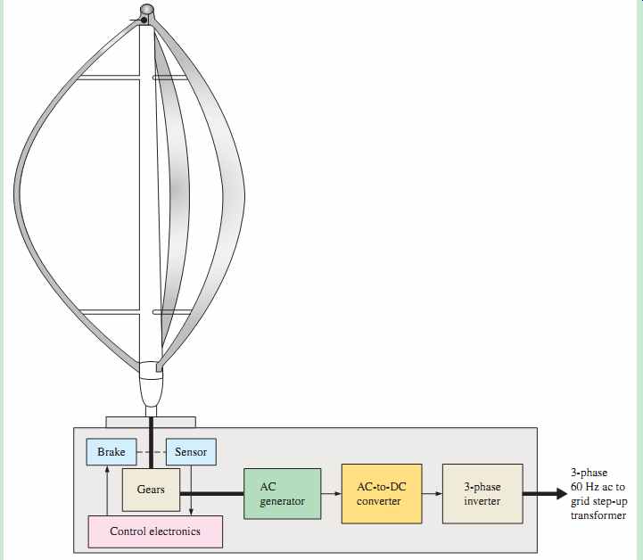
FIGURE GA-1 Diagram of a Darrieus or "eggbeater" VAWT. The size
of the blade assembly is disproportionately small compared to the base,
for the purpose of showing the block diagram.
Darrieus or Eggbeater Turbine
Figure GA-1 shows one type of VAWT called a Darrieus, named after its inventor, but is more commonly known as an "eggbeater" turbine.
VAWTs are difficult to mount on tall towers, so they are usually closer to the ground, thus requiring less support structure than HAWTs. Since the wind speed tends to be less at lower altitudes, the wind energy available is less than for a comparable-sized HAWT. Also, air flow near the ground is usually more turbulent causing more stress on the turbine.
Notice that the block diagram is similar to that of the HAWT but is usually a bit simpler in terms of the control electronics. Since there is no requirement for yawing the turbine to move it into the wind, the electronics may simply detect the rotational speed of the shaft and slow or stop the blades when the wind speed reaches a specified level.
In practice, the Darrieus VAWT is typically less efficient than the propeller-driven HAWT because it does not handle variations in wind speed as effectively. Also, it is more difficult to protect the Darrieus from excessive wind speeds without completely shutting it down. It also has a lower starting torque and does not self-start very well, so an auxiliary starting motor may be required.
Giromill Turbine
This turbine is a subtype of the Darrieus. Instead of curved blades, the giromill uses two or more straight airfoils (blades). A three-blade unit is shown in Figure GA6-2. Although it is cheaper and easier to build than a standard Darrieus turbine, it is less efficient, requires strong winds or a motor to start, and often cannot maintain a steady rate of rotation. A variation of this type of turbine has variable pitch airfoils for improvement of starting torque and reduction in torque pulsation due to uneven rotation rate.
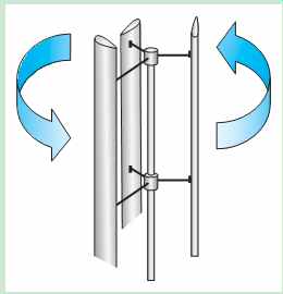
FIGURE GA-2 A giromill turbine.
Savonius Turbines
This is one of the simplest turbines but the least efficient.
Aerodynamically, Savonius turbines are drag-type turbines because, as they rotate, the scoops have to move air out of the way whereas blade-type turbines work on the principle of aerodynamic lift. One form of a two-scoop turbine is shown in Figure GA6-3; some times three or more scoops are used. The Savonius turbine is generally limited to small power applications. In the figure, the rotation is clockwise with the wind direction as shown.
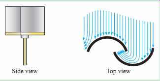
FIGURE GA-3 A form of Savonius VAWT.
Helical Wind Turbines Another variation of the Darrieus, the helical VAWT, has blades that are shaped in a twisted helical pattern. Some advantages are that the helical turbine tends to rotate more quietly that other types of blade turbines. Also, the helical turbine can withstand much higher wind speeds than other turbines and can begin rotation at much lower wind speeds than other types of VAWTs. A photo of one type of helical con figuration is shown in Figure GA6-4(a). Other forms of helix turbines are also used, as shown in part (b).
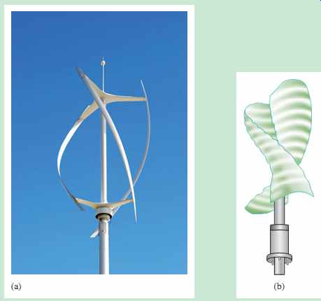
FIGURE GA-4 Two types of helical turbine.
A typical power curve for a typical helical turbine is shown in Figure GA6-5. Most wind turbines exhibit a similar-shaped power curve. Notice that the shape in the figure is very similar to that for the HAWT although the variable values are different for the lower power VAWT.
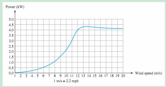
FIGURE GA-5 Power curve for helical wind turbine.
Questions:
1. What does VAWT stand for?
2. What are the basic types of VAWT?
3. What are some advantages and disadvantages when comparing HAWTs and VAWTs?
4. What type of wind turbine would you select to power a small home? Why?
---------