AMAZON multi-meters discounts AMAZON oscilloscope discounts
cont. from part 1
-------------------
Application Activity: Temperature to Voltage Conversion
The focus of this Application Activity is a temperature-sensing circuit that converts the temperature of a liquid to a proportional voltage for the purpose of maintaining the temperature of the liquid within a specified range. FIG. 28 illustrates the temperature-control system.
The temperature sensor is a thermistor, which is a device whose resistance changes with temperature. The thermistor is connected to a transistor circuit that is biased for linear operation. The output voltage of the circuit is proportional to the thermistor resistance and thus to the temperature of the liquid in the tank. The output voltage goes to an interface circuit that controls the valve to control the flow of fuel to the burner based on the voltage. If the temperature of the liquid is below a set value, the fuel is increased and if it is above that value, the fuel is decreased. The temperature is to be maintained at 70°C ; 5°C.
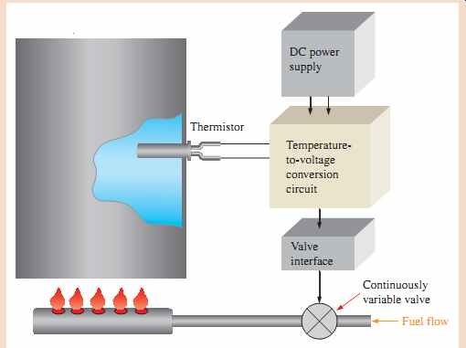
FIG. 28 Temperature-control system.
Designing the Circuit
Circuit Configuration
A voltage-divider biased linear amplifier is used for the temperature to-voltage conversion. The thermistor is used as one of the resistors in the voltage-divider bias. This thermistor has a positive temperature coefficient so, if the temperature increases, the resistance of the thermistor increases and if the temperature decreases, the resistance decreases. The base voltage changes proportionally to the change in thermistor resistance.
The output voltage is inversely proportional to the base voltage, so as the temperature goes up, the output voltage decreases and reduces the fuel flow to the burner. As the temperature goes down, the output voltage increases and allows more fuel to the burner.
Components
As shown in FIG. 29(a), the circuit is implemented with a 2N3904 transistor, three resistors and a thermistor with the values shown, and a +9 V dc source.
The thermistor has the temperature characteristic shown in part (b).
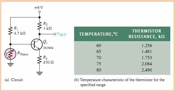
FIG. 29 Temperature-to-voltage conversion circuit.
1. Plot a graph of the thermistor temperature characteristic.
2. Refer to FIG. 29 and calculate the emitter and collector currents for each temperature shown.
3. Calculate the output voltage for each temperature shown in FIG. 29.
Simulation
The temperature-to-voltage conversion circuit is simulated to determine how the output voltage changes with temperature, as shown in FIG. 30. The thermistor is represented by a resistor with values corresponding to each specified temperature.
4. Compare your calculations for the output voltage with the simulated values.
Prototyping and Testing
Now that all the components have been selected, the prototype circuit is constructed and tested.
After the circuit is successfully tested, it is ready to be finalized on a printed circuit board.
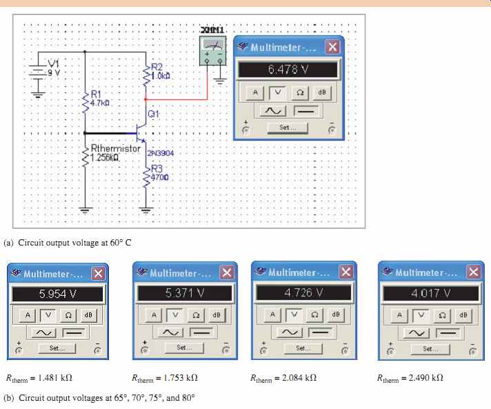
FIG. 30 Operation of the temperature-to-voltage conversion circuit over
temperature.
The Printed Circuit Board
A partially completed printed circuit board is shown in FIG. 31. Indicate how you would add conductive traces to complete the circuit and show the input/output terminal functions.
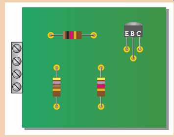
FIG. 31 Partially complete temperature con version circuit PC board.
SUMMARY OF TRANSISTOR BIAS CIRCUITS
npn transistors are shown. Supply voltage polarities are reversed for pnp transistors.
VOLTAGE-DIVIDER BIAS
EMITTER BIAS
COLLECTOR-FEEDBACK BIAS
BASE BIAS
EMITTER-FEEDBACK BIAS
SUMMARY
Section 1
-- The purpose of biasing a circuit is to establish a proper stable dc operating point (Q-point).
-- The Q-point of a circuit is defined by specific values for IC and VCE. These values are called the coordinates of the Q-point.
-- A dc load line passes through the Q-point on a transistor's collector curves intersecting the vertical axis at approximately IC(sat) and the horizontal axis at VCE(off).
-- The linear (active) operating region of a transistor lies along the load line below saturation and above cutoff.
Section 2
-- Loading effects are neglected for a stiff voltage divider.
-- The dc input resistance at the base of a BJT is approximately b_DC RE.
-- Voltage-divider bias provides good Q-point stability with a single-polarity supply voltage. It is the most common bias circuit.
Section 3
-- Emitter bias generally provides good Q-point stability but requires both positive and negative supply voltages.
-- The base bias circuit arrangement has poor stability because its Q-point varies widely with bDC.
-- Emitter-feedback bias combines base bias with the addition of an emitter resistor.
-- Collector-feedback bias provides good stability using negative feedback from collector to base.
TERMINOLOGY
DC load line-- A straight line plot of IC and VCE for a transistor circuit.
Feedback --The process of returning a portion of a circuit's output back to the input in such a way as to oppose or aid a change in the output.
Linear region-- The region of operation along the load line between saturation and cutoff.
Q-point-- The dc operating (bias) point of an amplifier specified by voltage and current values.
Stiff voltage divider --A voltage divider for which loading effects can be neglected.
TRUE/FALSE
1. DC bias establishes the dc operating point for an amplifier.
2. Q-point is the quadratic point in a bias circuit.
3. The dc load line intersects the horizontal axis of a transistor characteristic curve at VCE = VCC.
4. The dc load line intersects the vertical axis of a transistor characteristic curve at IC = 0.
5. The linear region of a transistor's operation lies between saturation and cutoff.
6. Voltage-divider bias is rarely used.
7. Input resistance at the base of the transistor can affect voltage-divider bias.
8. Stiff voltage-divider bias is essentially independent of base loading.
9. Emitter bias uses one dc supply voltage.
10. Negative feedback is employed in collector-feedback bias.
11. Base bias is less stable than voltage-divider bias.
12. A pnp transistor requires bias voltage polarities opposite to an npn transistor.
CIRCUIT-ACTION QUIZ
1. If VBB in FIG. 7 is increased, the Q-point value of collector current will (a) increase (b) decrease (c) not change
2. If VBB in FIG. 7 is increased, the Q-point value of VCE will (a) increase (b) decrease (c) not change
3. If the value of R2 in FIG. 10 is reduced, the base voltage will (a) increase (b) decrease (c) not change
4. If the value of R1 in FIG. 10 is increased, the emitter current will (a) increase (b) decrease (c) not change
5. If RE in FIG. 15 is decreased, the collector current will (a) increase (b) decrease (c) not change
6. If RB in FIG. 18 is reduced, the base-to-emitter voltage will (a) increase (b) decrease (c) not change
7. If VCC in FIG. 20 is increased, the base-to-emitter voltage will (a) increase (b) decrease (c) not change
8. If R1 in FIG. 24 opens, the collector voltage will (a) increase (b) decrease (c) not change
9. If R2 in FIG. 24 opens, the collector voltage will (a) increase (b) decrease (c) not change
10. If R2 in FIG. 24 is increased, the emitter current will (a) increase (b) decrease (c) not change
SELF-TEST
Section 1
The maximum value of collector current in a biased transistor is (a) (b) IC(sat) (c) greater than IE (d)
2. Ideally, a dc load line is a straight line drawn on the collector characteristic curves between (a) the Q-point and cutoff (b) the Q-point and saturation (c) VCE(cutoff) and IC(sat) (d)
3. If a sinusoidal voltage is applied to the base of a biased npn transistor and the resulting sinusoidal collector voltage is clipped near zero volts, the transistor is (a) being driven into saturation (b) being driven into cutoff (c) operating nonlinearly (d) answers (a) and (c) (e) answers (b) and (c)
Section 2
The input resistance at the base of a biased transistor depends mainly on (a) (b) RB (c) RE (d)
5. In a voltage-divider biased transistor circuit such as in FIG. 13, RIN(BASE) can generally be neglected in calculations when (a) (b) (c) (d)
6. In a certain voltage-divider biased npn transistor, VB is 2.95 V. The dc emitter voltage is approximately (a) 2.25 V (b) 2.95 V (c) 3.65 V (d) 0.7 V
7. Voltage-divider bias (a) cannot be independent of (b) can be essentially independent of (c) is not widely used (d) requires fewer components than all the other methods
Section 3
8. Emitter bias is (a) essentially independent of (b) very dependent on (c) provides a stable bias point (d) answers (a) and (c)
9. In an emitter bias circuit,
The emitter current (a) is 5.3 mA (b) is 2.7 mA (c) is 180 mA (d) cannot be determined
10. The disadvantage of base bias is that (a) it is very complex (b) it produces low gain (c) it is too beta dependent (d) it produces high leakage current
11. Collector-feedback bias is (a) based on the principle of positive feedback (b) based on beta multiplication (c) based on the principle of negative feedback (d) not very stable
Section 4
12. In a voltage-divider biased npn transistor, if the upper voltage-divider resistor (the one connected to VCC) opens, (a) the transistor goes into cutoff (b) the transistor goes into saturation (c) the transistor burns out (d) the supply voltage is too high
13. In a voltage-divider biased npn transistor, if the lower voltage-divider resistor (the one connected to ground) opens, (a) the transistor is not affected (b) the transistor may be driven into cutoff (c) the transistor may be driven into saturation (d) the collector current will decrease
14. In a voltage-divider biased pnp transistor, there is no base current, but the base voltage is approximately correct. The most likely problem(s) is (a) a bias resistor is open (b) the collector resistor is open (c) the base-emitter junction is open (d) the emitter resistor is open (e) answers (a) and (c) (f) answers (c) and (d) RE = 2.7 k OHM and VEE = 15 V.
bDC bDC bDC bDC
R1 V R2 RIN(BASE) 7 10R2 R2 7 10RIN(BASE) RIN(BASE) 7 R2 bDC and RE bDC IB = 0 and IB = IC>bDC IE - IB bDCIB
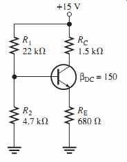
15. If R1 in FIG. 25 is open, the base voltage is (a) +10 V (b) 0 V (c) 3.13 V (d) 0.7 V 16. If R1 is open, the collector current in FIG. 25 is (a) 5.17 mA (b) 10 mA (c) 4.83 mA (d) 0 mA
PROBLEMS
Answers to all odd-numbered problems are at the end of the book.
BASIC PROBLEMS
Section 1--The DC Operating Point
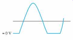
1. The output (collector voltage) of a biased transistor amplifier is shown in FIG. 32. Is the transistor biased too close to cutoff or too close to saturation?
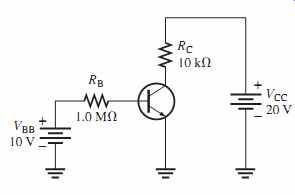
2. What is the Q-point for a biased transistor as in FIG. 2 with
3. What is the saturation value of collector current in Problem 2?
4. What is the cutoff value of VCE in Problem 2?
5. Determine the intercept points of the dc load line on the vertical and horizontal axes of the collector-characteristic curves for the circuit in FIG. 33.
VCC = 18 V, and RC = 1.0 k OHM? IB = 150 mA, bDC = 75,
Multisim file circuits are identified with a logo and are in the Problems folder on the companion website.
Filenames correspond to figure numbers (e.g., F05-33).
6. Assume that you wish to bias the transistor in FIG. 33 with To what voltage must you change the VBB supply? What are IC and VCE at the Q-point, given that
7. Design a biased-transistor circuit using VBB = VCC = 10 V for a Q-point of IC _ 5 mA and VCE = 4 V. Assume The design involves finding RB, RC, and the minimum power rating of the transistor. (The actual power rating should be greater.) Sketch the circuit.
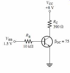
8. Determine whether the transistor in FIG. 34 is biased in cutoff, saturation, or the linear region. Remember that is valid only in the linear region.
IC = bDCIB bDC = 100.
bDC = 50? IB = 20 mA.
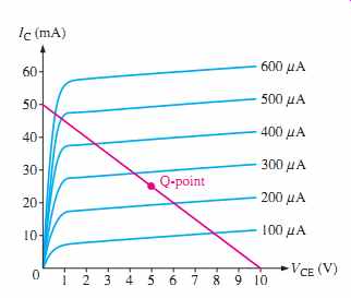
9. From the collector characteristic curves and the dc load line in FIG. 35, determine the following:
(a) Collector saturation current (b) VCE at cutoff (c) Q-point values of IB, IC, and VCE
10. From FIG. 35 determine the following:
(a) Maximum collector current for linear operation (b) Base current at the maximum collector current (c) VCE at maximum collector current
Section 2 Voltage-Divider Bias
11. What is the minimum value of in FIG. 36 that makes
12. The bias resistor R2 in FIG. 36 is replaced by a potentiometer. What minimum resistance setting causes saturation?
13. If the potentiometer described in Problem 12 is set at what are the values for IC and VCE?
14. Determine all transistor terminal voltages with respect to ground in FIG. 37.
15. Show the connections required to replace the transistor in FIG. 37 with a pnp device.
16. (a) Determine VB in FIG. 38.
(b) How is VB affected if the transistor is replaced by one with a 17. Determine the following in FIG. 38:
(a) Q-point values (b) The minimum power rating of the transistor 18. Determine I1, I2, and IB in FIG. 38.
bDC of 50? 2k OHM, 15 k OHM RIN(BASE) G 10R2? bDC
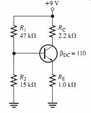
FIG. 37
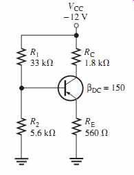
FIG. 38
Section 3 Other Bias Methods
19. Analyze the circuit in FIG. 39 to determine the correct voltages at the transistor terminals with respect to ground. Assume
20. To what value can RE in FIG. 39 be reduced without the transistor going into saturation?
21. Taking VBE into account in FIG. 39, how much will IE change with a temperature increase from The VBE is 0.7 V at and decreases 2.5 mV per degree Celsius.
Neglect any change in
22. When can the effect of a change in be neglected in the emitter bias circuit?
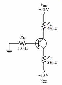
23. Determine IC and VCE in the pnp emitter bias circuit of FIG. 40. Assume
24. Determine VB, VC, and IC in FIG. 41.
bDC = 100.
bDC bDC.
25°C 25°C to 100°C? bDC = 100.
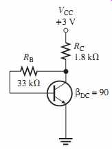
FIG. 41
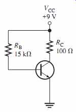
FIG. 42
25. What value of RC can be used to decrease IC in Problem 24 by 25 percent?
26. What is the minimum power rating for the transistor in Problem 25?
27. A collector-feedback circuit uses an npn transistor with
Determine the collector current and the collector voltage if
28. Determine IB, IC, and VCE for a base-biased transistor circuit with the following values:
VCC = 12 V,
29. If in Problem 28 doubles over temperature, what are the Q-point values?
30. You have two base bias circuits connected for testing. They are identical except that one is biased with a separate VBB source and the other is biased with the base resistor connected to VCC.
Ammeters are connected to measure collector current in each circuit. You vary the VCC supply voltage and observe that the collector current varies in one circuit, but not in the other. In which circuit does the collector current change? Explain your observation.
31. The datasheet for a particular transistor specifies a minimum of 50 and a maximum of 125. What range of Q-point values can be expected if an attempt is made to mass-produce the circuit in FIG. 42? Is this range acceptable if the Q-point must remain in the transistor's linear region?
32. The base bias circuit in FIG. 42 is subjected to a temperature variation from
The decreases by 50 percent at and increases by 75 percent at from its nominal value of 110 at What are the changes in IC and VCE over the temperature range of
0°C to 70°C? 25°C.
70°C 0°C bDC
0°C to 70°C.
bDC bDC bDC RB = 22 k OHM, and RC = 100 OHM. bDC = 90, bDC = 200. RB = 47 k OHM.
VCC = 12 V, RC = 1.2 k OHM, and
Section 4 Troubleshooting
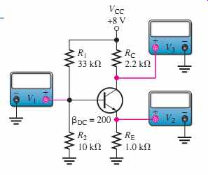
33. Determine the meter readings in FIG. 43 if R1 is open.
34. Assume the emitter becomes shorted to ground in FIG. 43 by a solder splash or stray wire clipping. What do the meters read? When you correct the problem, what do the meters read? 35. Determine the most probable failures, if any, in each circuit of FIG. 44, based on the indicated measurements.
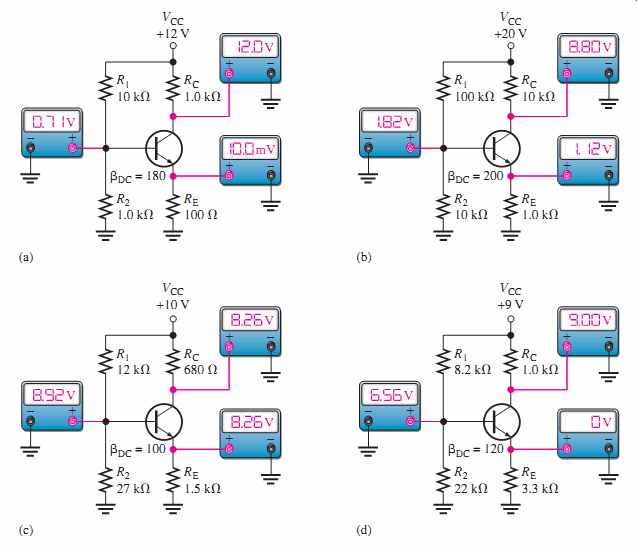
FIG. 44
36. Determine if the DMM readings 2 through 4 in the breadboard circuit of FIG. 45 are cor rect. If they are not, isolate the problem(s). The transistor is a pnp device with a specified dc beta range of 35 to 100.
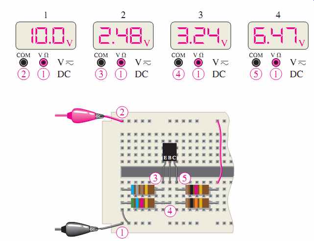
FIG. 45
37. Determine each meter reading in FIG. 45 for each of the following faults:
(a) the resistor open (b) the resistor open (c) the resistor open (d) the resistor open (e) a short from emitter to ground (f ) an open base-emitter junction 1.0 k OHM 10 k OHM 5.6 k OHM 680 OHM
APPLICATION ACTIVITY PROBLEMS
38. Determine VB, VE, and VC in the temperature-to-voltage conversion circuit in FIG. 29(a) if R1 fails open.
39. What faults will cause the transistor in the temperature-to-voltage conversion circuit to go into cutoff?
40. A thermistor with the characteristic curve shown in FIG. 46 is used in the circuit of FIG. 29(a). Calculate the output voltage for temperatures of Assume a stiff voltage divider.
41. Explain how you would identify an open collector-base junction in the transistor in FIG. 29(a).
45°C, 48°C, and 53°C.
FIG. 46
DATASHEET PROBLEMS
42. Analyze the temperature-to-voltage conversion circuit in FIG. 47 at the temperature extremes indicated on the graph in FIG. 46 for both minimum and maximum specified datasheet values of hFE. Refer to the partial datasheet in FIG. 48.
43. Verify that no maximum ratings are exceeded in the temperature-to-voltage conversion circuit in FIG. 47. Refer to the partial datasheet in FIG. 48.
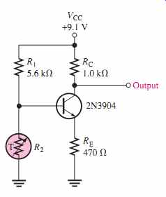
FIG. 47
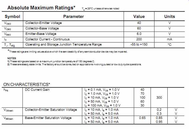
FIG. 48 Partial datasheet for the 2N3904 transistor. Copyright Fairchild Semiconductor Corporation.
44. Refer to the partial datasheet in FIG. 49.
(a) What is the maximum collector current for a 2N2222A? (b) What is the maximum reverse base-emitter voltage for a 2N2218A?
45. Determine the maximum power dissipation for a 2N2222A at
46. When you increase the collector current in a 2N2219A from 1 mA to 500 mA, how much does the minimum (hFE) change?
ADVANCED PROBLEMS
47. Design a circuit using base bias that operates from a 15 V dc voltage and draws a maximum current from the dc source (ICC(max)) of 10 mA. The Q-point values are to be IC = 5 mA and VCE =5 V. The transistor is a 2N3904. Assume a midpoint value for bDC.
bDC 100°C.
FIG. 49 Partial datasheet for 2N2218A-2N2222A.
48. Design a circuit using emitter bias that operates from dc voltages of +12 V and The maximum ICC is to be 20 mA and the Q-point is at 10 mA and 4 V. The transistor is a 2N3904.
49. Design a circuit using voltage-divider bias for the following specifications: VCC _ 9 V, ICC(max)
= 5 mA, IC = 1.5 mA, and VCE = 3 V. The transistor is a 2N3904.
50. Design a collector-feedback circuit using a 2N2222A with VCC = 5 V, IC = 10 mA, and VCE = 1.5 V.
51. Can you replace the 2N3904 in FIG. 47 with a 2N2222A and maintain the same range of output voltage over a temperature range from 52. Refer to the datasheet graph in FIG. 50 and the partial datasheet in FIG. 49. Determine the minimum dc current gain for a 2N2222A at for VCE = 1 V. -55°C, 25°C, and 175°C 45°C to 55°C?
-12 V.
FIG. 50
53. A design change is required in the valve interface circuit of the temperature-control system shown in FIG. 28. The new design will have a valve interface input resistance of
Determine the effect this change has on the temperature-to-voltage conversion circuit.
54. Investigate the feasibility of redesigning the temperature-to-voltage conversion circuit in FIG. 29 to operate from a dc supply voltage of 5.1 V and produce the same range of output volt ages determined in the Application Activity over the required thermistor temperature range from 60°C to 80°C.
10 k OHM.
----------------
Green-Tech Application 5: Wind Power
Wind energy, like solar energy, is a major renewable resource. Wind is actually a product of solar energy because differences in earth temperatures result in the movement of air.
Wind turbines harvest energy from the wind and may be used as small single units to supply an individual home or wind farms where tens to hundreds of large units harvest wind energy and convert it to electricity.
Two key elements in a wind turbine are the blades and the ac generator. In many wind turbines, electronic circuits sense the wind direction and speed and adjust the orientation and pitch of the blades to maximize the energy collected from the wind. The generator produces a varying ac voltage that depends on the rotational speed of the blades due to the wind. Since the frequency and amplitude of a generator output varies with wind speed, the ac output is converted to dc and then back to 60 Hz ac with an inverter. Like a solar power system, the energy can be stored in batteries using a charge controller for smaller applications, or the energy can be connected directly to the grid for large-scale applications.
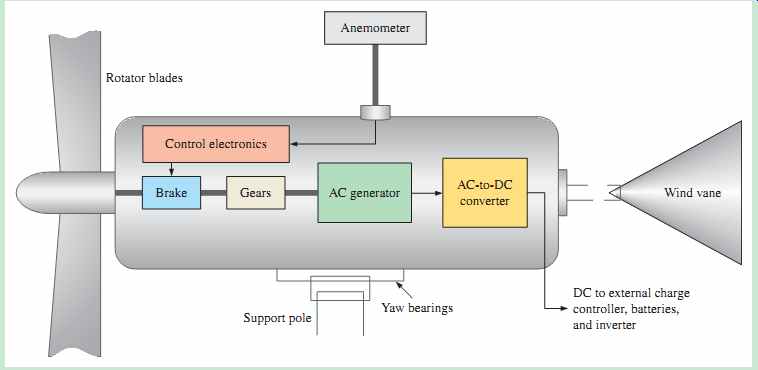
FIG. G-1 Basic small HAWT system operation.
FIG. G-1 shows a basic diagram of a horizontal-axis wind turbine (HAWT) for small power applications, such as home use. A typical wind turbine has three blades and is mounted on a very high support tower. Wind energy is converted to mechanical energy by the rotating blades. As shown in FIG. G-1, the blade rotation is applied to a shaft, which is geared up to turn the ac generator shaft at a higher rate than the blades are rotating. The generator rotation produces an ac voltage output with a frequency that depends on the rate of rotation. Since it is a variable frequency and amplitude output, as previously mentioned, the ac is converted to dc by the ac-to-dc converter. The dc is sent to a charge controller that charges the storage batteries. The battery output is applied to an inverter where it is converted to a 120 V, 60 Hz ac voltage for individual consumer use.
The wind vane and yaw bearing assembly are used on small turbines to keep the blades pointed into the wind. An anemometer senses the wind speed in order to brake the blades when the wind reaches a specified speed. This prevents mechanical damage if the wind speed is too high.
The AC-to-DC Converter Because of the variable frequency of the ac from the generator, it must first be converted to dc for the charge controller. A rectifier and regulator are used for the conversion, as illustrated in FIG. G-2. The ac voltage from the generator varies in amplitude and frequency as a function of wind speed. The ac-to-dc converter changes the varying ac to a varying dc voltage, which is then applied to a voltage regulator to produce a specified constant dc voltage, as shown.
Large-Scale Wind Turbines
FIG. G-3 is a horizontal axis grid-tie turbine, which is the most common configuration for commercial wind farm applications. The wind direction sensor sends a signal to the control electronics so the yaw motor can keep the turbine pointing into the wind. The wind speed sensor sends a signal to the control electronics so the pitch of the blades can be adjusted for maximum efficiency. Also, when the wind exceeds a specified speed, the control electronics activates the brakes to reduce or stop rotation of the blades, preventing damage to the unit.

FIG. G-2 AC-to-DC converter block diagram.
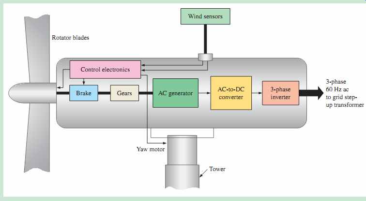
FIG. G-3 Large horizontal-axis wind turbine (HAWT).
For large wind turbines (above 100 kW-150 kW) the voltage generated is usually 690 V three-phase ac. The output goes to a transformer usually located in the tower or near its base and is stepped up to thousands of volts depending on the requirements of the local electrical grid.
Power in the Wind
The amount of power available in the wind can be calculated using the following formula:
P = pAv^3/2
In the formula, p is the density of the air, A is the area swept by the blades, and v is the velocity (speed) of the wind. Note that the power is dependent on the length of the blades, r, and the cube of the wind speed, v^3. Since A =pi r^2, if the length of the blades is doubled, the available power in the wind will be increased by four times (2^2 = 4). If the wind velocity doubles, the available power in the wind is increased by eight times (2^3 = 8). Of course, a turbine cannot convert all of the available wind power into mechanical power to turn the generator. In fact, most practical turbines can convert less than 50% of the wind power. FIG. G-4 illustrates the factors that affect the amount of power that can be extracted from the wind.
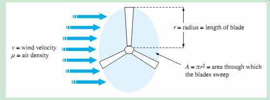
FIG. G-4 Factor determining the available power in the wind.
Betz Law
This law states that the theoretical limit of the amount of power that can be extracted from the wind is 59% if all conditions are perfect. This limiting factor was developed by Albert Betz in 1926. In practice, 20% to 40% can normally be expected.
Wind Power Curve
A wind power curve shows the amount of power that can be extracted over a range of wind speeds (velocities) for specific turbines. Wind power curves will vary from one type of turbine to another. FIG. G-5 shows a typical curve. The cut-in speed is the wind speed at which the blades begin to turn. The start-up speed is the wind speed at which the blades are moving fast enough to cause the generator to produce electricity. The start-up speed is slightly higher than the cut-in speed. The maximum power output is the peak power that the turbine can produce. For this example curve, the maximum power output is approximately 200 kW at a wind speed of approximately 28 mph.
To limit the rotational speed of the blades above the maximum power output (MPO) point in order to prevent damage to the machine, a process called furling is used. Ideally, the curve is kept as level as possible as shown by the dashed portion of the curve in FIG. G-5.
However, in practice, the power decreases above that point, once the furling process is activated. Furling can be accomplished by changing the pitch of the blades or turning the entire turbine away from the wind direction slightly under direction of the control electronics. Also, when the wind reaches a predetermined maximum, the turbine can be completely shut down.
For example, the curve shows this turbine being shut downat45 mph.
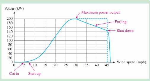
FIG. G-5 Example of a wind power curve for a wind turbine.
Questions
Some questions may require research beyond the content of this coverage. Answers are at the end of the book.
1. What does HAWT stand for?
2. Why does the input voltage to the ac-to-dc converter vary in amplitude and frequency?
3. What are the physical factors that determine the amount of power available in the wind that strikes the blades of a turbine?
4. What is the Betz limit?
5. In wind farms, how close together should the turbines generally be placed?
------------------
