AMAZON multi-meters discounts AMAZON oscilloscope discounts
OUTLINE
--1 The Class A Power Amplifier [this page, below]
--2 The Class B and Class AB Push-Pull Amplifiers [this page, below]
--4 Troubleshooting Application Activity
GOALS
-- Explain and analyze the operation of class A amplifiers
-- Explain and analyze the operation of class B and class AB amplifiers
-- Explain and analyze the operation of class C amplifiers
-- Troubleshoot power amplifiers
TERMINOLOGY
-- Class A
-- Class B
-- Class AB
-- Class C
-- Push-pull
-- Power gain
-- Efficiency
APPLICATION ACTIVITY PREVIEW
The Application Activity in this is a public address system. Recall that the complete system includes the preamplifier, a power amplifier, and a dc power supply. You will focus on the power amplifier in this section and complete the total system by combining the three component parts.
INTRODUCTION
Power amplifiers are large-signal amplifiers. This generally means that a much larger portion of the load line is used during signal operation than in a small-signal amplifier. In this section, we will cover four classes of power amplifiers: class A, class B, class AB, and class C. These amplifier classifications are based on the percentage of the input cycle for which the amplifier operates in its linear region. Each class has a unique circuit configuration because of the way it must be operated. The emphasis is on power amplification.
Power amplifiers are normally used as the final stage of a communications receiver or transmitter to provide signal power to speakers or to a transmitting antenna. BJTs are used to illustrate power amplifier principles.
----
1. THE CLASS A POWER AMPLIFIER
When an amplifier is biased such that it always operates in the linear region where the output signal is an amplified replica of the input signal, it is a class A amplifier. The discussion of amplifiers in the previous sections apply to class A operation. Power amplifiers are those amplifiers that have the objective of delivering power to a load. This means that components must be considered in terms of their ability to dissipate heat.
After completing this section, you should be able to:
-- Explain and analyze the operation of class A amplifiers
-- Discuss transistor heat dissipation
-- Describe the purpose of a heat sink
-- Discuss the importance of a centered Q-point
-- Describe the relationship of the dc and ac load lines with the Q-point
-- Describe the effects of a non-centered Q-point on the output waveform
-- Determine power gain
-- Define dc quiescent power
-- Discuss and determine output signal power
-- Define and determine the efficiency of a power amplifier
----
In a small-signal amplifier, the ac signal moves over a small percentage of the total ac load line. When the output signal is larger and approaches the limits of the ac load line, the amplifier is a large-signal type. Both large-signal and small-signal amplifiers are considered to be class A if they operate in the linear region at all times, as illustrated in FIG. 1.
Class A power amplifiers are large-signal amplifiers with the objective of providing power (rather than voltage) to a load. As a rule of thumb, an amplifier may be considered to be a power amplifier if it is rated for more than 1 W and it is necessary to consider the problem of heat dissipation in components.

FIG. 1 Basic class A amplifier operation. Output is shown 180° out of phase
with the input (inverted).
Heat Dissipation
Power transistors (and other power devices) must dissipate a large amount of internally generated heat. For BJT power transistors, the collector terminal is the critical junction; for this reason, the transistor's case is always connected to the collector terminal. The case of all power transistors is designed to provide a large contact area between it and an external heat sink. Heat from the transistor flows through the case to the heat sink and then dissipates in the surrounding air. Heat sinks vary in size, number of fins, and type of material.
Their size depends on the heat dissipation requirement and the maximum ambient temperature in which the transistor is to operate. In high-power applications (a few hundred watts), a cooling fan may be necessary.
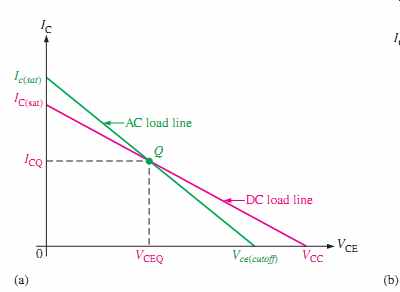
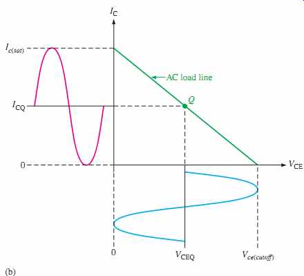
FIG. 2 Maximum class A output occurs when the Q-point is centered on the
ac load line.
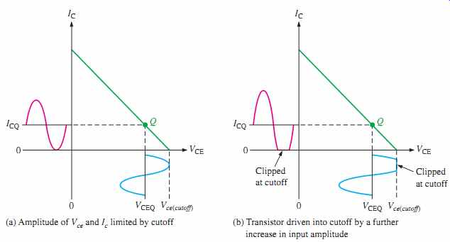
FIG. 3 Q-point closer to cutoff. (a) Amplitude of Vce and Ic limited by cutoff
(b) Transistor driven into cutoff by a further increase in input amplitude
Centered Q-Point
Recall that the dc and ac load lines intersect at the Q-point. When the Q-point is at the center of the ac load line, a maximum class A signal can be obtained. You can see this concept by examining the graph of the load line for a given amplifier in FIG. 2(a). This graph shows the ac load line with the Q-point at its center. The collector current can vary from its Q-point value, ICQ, up to its saturation value, Ic(sat), and down to its cutoff value of zero.
Likewise, the collector-to-emitter voltage can swing from its Q-point value, VCEQ, up to its cutoff value, Vce(cutoff ), and down to its saturation value of near zero. This operation is indicated in FIG. 2(b). The peak value of the collector current equals ICQ, and the peak value of the collector-to-emitter voltage equals VCEQ in this case. This signal is the maxi mum that can be obtained from the class A amplifier. Actually, the output cannot quite reach saturation or cutoff, so the practical maximum is slightly less.
If the Q-point is not centered on the ac load line, the output signal is limited. FIG. 3 shows an ac load line with the Q-point moved away from center toward cutoff. The output variation is limited by cutoff in this case. The collector current can only swing down to near zero and an equal amount above ICQ. The collector-to-emitter voltage can only swing up to its cutoff value and an equal amount below VCEQ. This situation is illustrated in FIG. 3(a). If the amplifier is driven any further than this, it will "clip" at cutoff, as shown in FIG. 3(b).
FIG. 4 shows an ac load line with the Q-point moved away from center toward saturation. In this case, the output variation is limited by saturation. The collector current can only swing up to near saturation and an equal amount below ICQ. The collector-to-emitter voltage can only swing down to its saturation value and an equal amount above VCEQ. This situation is illustrated in FIG. 4(a). If the amplifier is driven any further, it will "clip" at saturation, as shown in FIG. 4(b).
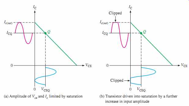
FIG. 4 Q-point closer to saturation. (a) Amplitude of Vce and Ic limited
by saturation (b) Transistor driven into saturation by a further increase
in input amplitude.
Power Gain
A power amplifier delivers power to a load. The power gain of an amplifier is the ratio of the output power (power delivered to the load) to the input power. In general, power gain is
[EQN. 1] Ap = P_L/P_in
where Ap is the power gain, PL is signal power delivered to the load, and Pin is signal power delivered to the amplifier.
The power gain can be computed by any of several formulas, depending on what is known. Frequently, the easiest way to obtain power gain is from input resistance, load resistance, and voltage gain. To see how this is done, recall that power can be expressed in terms of voltage and resistance as
P=V^2/R
For ac power, the voltage is expressed as rms. The output power delivered to the load is:
P_L=V^2 L / R-L
The input power delivered to the amplifier is
P_in = V^2 in / R in
By substituting into EQN. 1, the following useful relationship is produced:

Since VL/Vin = Av,
Ap=A^2v[Rin/R_L]
EQN. 2
Recall from Section 6 that for a voltage-divider biased amplifier,
Rin(tot) = R1 ||7 R2 || Rin(base)
and that for a CE or CC amplifier,
Rin(base) = βac Re
EQN. 2 shows that the power gain of an amplifier is the voltage gain squared times the ratio of the input resistance to the output load resistance. The formula can be applied to any amplifier. For example, assume a common-collector (CC) amplifier has an input resistance of and a load resistance of Since a CC amplifier has a voltage gain of approximately 1, the power gain is:

For a CC amplifier, Ap is just the ratio of the input resistance to the output load resistance.
DC Quiescent Power
The power dissipation of a transistor with no signal input is the product of its Q-point cur rent and voltage.
P_DQ = I_CQ V_CEQ
The only way a class A power amplifier can supply power to a load is to maintain a quiescent current that is at least as large as the peak current requirement for the load current.
A signal will not increase the power dissipated by the transistor but actually causes less total power to be dissipated. The dc quiescent power, given in EQN. 3, is the maxi mum power that a class A amplifier must handle. The transistor's power rating must exceed this value.
Output Power
In general, the output signal power is the product of the rms load current and the rms load voltage. The maximum unclipped ac signal occurs when the Q-point is centered on the ac load line. For a CE amplifier with a centered Q-point, the maximum peak voltage swing is:
Vc(max) = ICQ Rc
The rms value is 0.707Vc(max).
The maximum peak current swing is
Ic(max) = V_CEQ/ R_C
The rms value is 0.707Ic(max).
To find the maximum signal power output, use the rms values of maximum current and voltage. The maximum power out from a class A amplifier is:
Pout(max) = (0.707Ic)(0.707Vc)
Pout(max)= 0.5 ICQ VCEQ
EQN. 4
------------- EXAMPLE 1
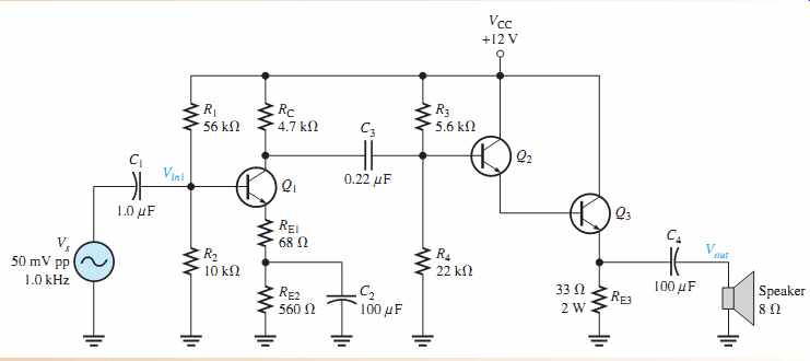
Determine the voltage gain and the power gain of the class A power amplifier in FIG. 5. Assume βac = 200 for all transistors.
--------------------
Efficiency
The efficiency of any amplifier is the ratio of the output signal power supplied to a load to the total power from the dc supply. The maximum output signal power that can be obtained is given by EQN. 4. The average power supply current, ICC, is equal to ICQ and the supply voltage is at least 2VCEQ. Therefore, the total dc power is
PDC = ICC VCC = 2 ICQ VCEQ
The maximum efficiency, of a capacitively coupled class A amplifier is:

The maximum efficiency of a capacitively coupled class A amplifier cannot be higher than 0.25, or 25%, and, in practice, is usually considerably less (about 10%). Although the efficiency can be made higher by transformer coupling the signal to the load, there are drawbacks to transformer coupling. These drawbacks include the size and cost of transformers as well as potential distortion problems when the transformer core begins to saturate. In general, the low efficiency of class A amplifiers limits their usefulness to small power applications that require usually less than 1 W.
--------
SECTION 1 CHECKUP
1. What is the purpose of a heat sink?
2. Which lead of a BJT is connected to the case?
3. What are the two types of clipping with a class A power amplifier?
4. What is the maximum efficiency for a class A amplifier?
5. How can the power gain of a CC amplifier be expressed in terms of a ratio of resistances?
--------
--------
2. THE CLASS B AND CLASS AB PUSH-PULL AMPLIFIERS
When an amplifier is biased at cutoff so that it operates in the linear region for of the input cycle and is in cutoff for 180° it is a class B amplifier. Class AB amplifiers are biased to conduct for slightly more than 180°.
The primary advantage of a class B or class AB amplifier over a class A amplifier is that either one is more efficient than a class A amplifier; you can get more output power for a given amount of input power. A disadvantage of class B or class AB is that it is more difficult to implement the circuit in order to get a linear reproduction of the input waveform. The term push-pull refers to a common type of class B or class AB amplifier circuit in which two transistors are used on alternating half-cycles to reproduce the input waveform at the output.
After completing this section, you should be able to:
-- Explain and analyze the operation of class B and class AB amplifiers
-- Describe class B operation
-- Discuss Q-point location
-- Describe class B push-pull operation
-- Discuss transformer coupling - Explain complementary symmetry transistors
-- Explain crossover distortion 180°.
-- Bias a push-pull amplifier for class AB operation
-- Define class AB - Explain class AB ac signal operation
-- Describe a single-supply push-pull amplifier
-- Discuss class B/AB power
-- Calculate maximum output power - Calculate dc input power
-- Determine efficiency
-- Determine the ac input resistance of a push-pull amplifier
-- Discuss the Darlington class AB amplifier
-- Determine ac input resistance
-- Describe the Darlington/complementary Darlington class AB amplifier
------
Class B Operation
The class B operation is illustrated in FIG. 6, where the output waveform is shown relative to the input in terms of time (t).
The Q-Point Is at Cutoff
The class B amplifier is biased at the cutoff point so that ICQ = 0 and VCEQ = VCE(cutoff).
It is brought out of cutoff and operates in its linear region when the input signal drives the transistor into conduction. This is illustrated in FIG. 7 with an emitter-follower circuit where the output is not a replica of the input.

FIG. 6 Basic class B amplifier operation (noninverting).
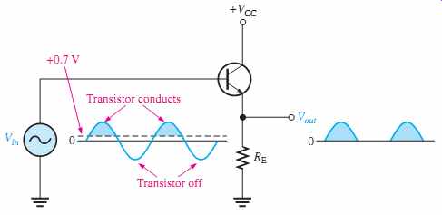
FIG. 7 Common-collector class B amplifier.
Class B Push-Pull Operation
As you can see, the circuit in FIG. 7 only conducts for the positive half of the cycle. To amplify the entire cycle, it is necessary to add a second class B amplifier that operates on the negative half of the cycle. The combination of two class B amplifiers working together is called push-pull operation.
There are two common approaches for using push-pull amplifiers to reproduce the entire waveform. The first approach uses transformer coupling. The second uses two complementary symmetry transistors; these are a matching pair of npn/pnp BJTs.
Transformer Coupling
Transformer coupling is illustrated in FIG. 8. The input transformer has a center-tapped secondary that is connected to ground, producing phase in version of one side with respect to the other. The input transformer thus converts the input signal to two out-of-phase signals for the transistors. Notice that both transistors are npn types. Because of the signal inversion, Q1 will conduct on the positive part of the cycle and Q2 will conduct on the negative part. The output transformer combines the signals by permitting current in both directions, even though one transistor is always cut off. The positive power supply signal is connected to the center tap of the output transformer.
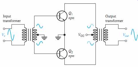
FIG. 8 Transformer-coupled push-pull amplifiers. Q1 conducts during the
positive half-cycle; Q2 conducts during the negative half-cycle. The two
halves are combined by the output transformer.
Complementary Symmetry Transistors
FIG. 9 shows one of the most popular types of push-pull class B amplifiers using two emitter-followers and both positive and negative power supplies. This is a complementary amplifier because one emitter-follower uses an npn transistor and the other a pnp, which conduct on opposite alternations of the input cycle. Notice that there is no dc base bias voltage (VB = 0). Thus, only the signal voltage drives the transistors into conduction. Transistor Q1 conducts during the positive half of the input cycle, and Q2 conducts during the negative half.
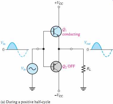
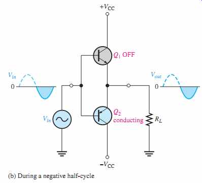
FIG. 9 Class B push-pull ac operation. (a) During a positive half-cycle (b)
During a negative half-cycle.
Crossover Distortion
When the dc base voltage is zero, both transistors are off and the input signal voltage must exceed VBE before a transistor conducts. Because of this, there is a time interval between the positive and negative alternations of the input when neither transistor is conducting, as shown in FIG. 10. The resulting distortion in the output waveform is called crossover distortion.
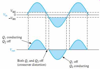
FIG. 10 Illustration of crossover distortion in a class B push-pull amplifier.
The transistors conduct only during portions of the input indicated by
the shaded areas.
Biasing the Push-Pull Amplifier for ClassAB Operation
To overcome crossover distortion, the biasing is adjusted to just overcome the VBE of the transistors; this results in a modified form of operation called class AB. In class AB operation, the push-pull stages are biased into slight conduction, even when no input signal is present. This can be done with a voltage-divider and diode arrangement, as shown in FIG. 11. When the diode characteristics of D1 and D2 are closely matched to the characteristics of the transistor base-emitter junctions, the current in the diodes and the current in the transistors are the same; this is called a current mirror. This current mirror produces the desired class AB operation and eliminates crossover distortion.
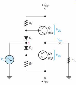
FIG. 11 Biasing the push-pull amplifier with current-mirror diode bias
to eliminate crossover distortion. The transistors form a complementary
pair (one npn and one pnp).
In the bias path of the circuit in FIG. 11, R1 and R2 are of equal value, as are the positive and negative supply voltages. This forces the voltage at point A (between the diodes) to equal 0 V and eliminates the need for an input coupling capacitor. The dc volt age on the output is also 0 V. Assuming that both diodes and both complementary transistors are identical, the drop across D1 equals the VBE of Q1, and the drop across D2 equals the VBE of Q2. Since they are matched, the diode current will be the same as ICQ. The diode current and ICQ can be found by applying Ohm's law to either R1 or R2 as follows:
ICQ = [VCC - 0.7 V]/ R1
This small current required of class AB operation eliminates the crossover distortion but has the potential for thermal instability if the transistor's VBE drops are not matched to the diode drops or if the diodes are not in thermal equilibrium with the transistors. Heat in the power transistors decreases the base-emitter voltage and tends to increase current. If the diodes are warmed the same amount, the current is stabilized; but if the diodes are in a cooler environment, they cause ICQ to increase even more. More heat is produced in an unrestrained cycle known as thermal runaway. To keep this from happening, the diodes should have the same thermal environment as the transistors. In some cases, a small resistor in the emitter of each transistor can alleviate thermal runaway.
Crossover distortion also occurs in transformer-coupled amplifiers like the one shown in FIG. 8. To eliminate it in this case, 0.7 V is applied to the input transformer's secondary that just biases both transistors into conduction. The bias voltage to produce this drop can be derived from the power supply using a single diode as shown in FIG. 12.
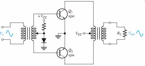
FIG. 12 Eliminating crossover distortion in a transformer-coupled push-pull
amplifier. The biased diode compensates for the base-emitter drop of the
transistors and produces class AB operation.
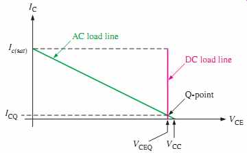
FIG. 13 Load lines for a complementary symmetry push-pull amplifier.
Only the load lines for the npn transistor are shown.
AC Operation
Consider the ac load line for Q1 of the class AB amplifier in FIG. 11.
The Q-point is slightly above cutoff. (In a true class B amplifier, the Q-point is at cutoff.) The ac cutoff voltage for a two-supply operation is at VCC with an ICQ as given earlier. The ac saturation current for a two-supply operation with a push-pull amplifier is:
Ic(sat) = VCC/RL [ EQN. 5]
The ac load line for the npn transistor is as shown in FIG. 13. The dc load line can be found by drawing a line that passes through VCEQ and the dc saturation current, IC(sat).
However, the saturation current for dc is the current if the collector to emitter is shorted on both transistors! This assumed short across the power supplies obviously would cause maximum current from the supplies and implies the dc load line passes almost vertically through the cutoff as shown. Operation along the dc load line, such as caused by thermal runaway, could produce such a high current that the transistors are destroyed.
FIG. 14(a) illustrates the ac load line for Q1 of the class AB amplifier in FIG. 14(b). In the case illustrated, a signal is applied that swings over the region of the ac load line shown in bold. At the upper end of the ac load line, the voltage across the transistor (Vce) is a minimum, and the output voltage is maximum.
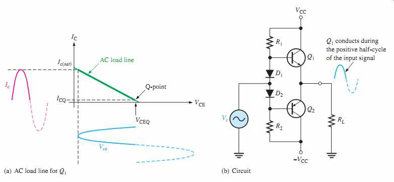
FIG. 14 (b) Circuit (a) AC load line for Q1
Under maximum conditions, transistors Q1 and Q2 are alternately driven from near cut off to near saturation. During the positive alternation of the input signal, the Q1 emitter is driven from its Q-point value of 0 to nearly VCC, producing a positive peak voltage a little less than VCC. Likewise, during the negative alternation of the input signal, the Q2 emitter is driven from its Q-point value of 0 V, to near –VCC, producing a negative peak voltage almost equal to –VCC. Although it is possible to operate close to the saturation current, this type of operation results in increased distortion of the signal.
The ac saturation current ( EQN. 5) is also the peak output current. Each transistor can essentially operate over its entire load line. Recall that in class A operation, the transistor can also operate over the entire load line but with a significant difference. In class A operation, the Q-point is near the middle and there is significant current in the transistors even with no signal. In class B operation, when there is no signal, the transistors have only a very small current and therefore dissipate very little power. Thus, the efficiency of a class B amplifier can be much higher than a class A amplifier. It will be shown later that the maximum efficiency of a class B amplifier is 79%.
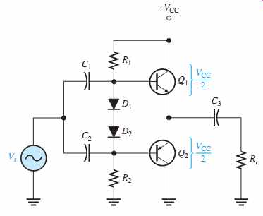
FIG. 16 Single-ended push-pull amplifier.
Single-Supply Push-Pull Amplifier
Push-pull amplifiers using complementary symmetry transistors can be operated from a single voltage source as shown in FIG. 16. The circuit operation is the same as that described previously, except the bias is set to force the output emitter voltage to be VCC 2 instead of zero volts used with two supplies. Because the output is not biased at zero volts, capacitive coupling for the input and output is necessary to block the bias voltage from the source and the load resistor. Ideally, the output voltage can swing from zero to VCC, but in practice it does not quite reach these ideal values.
Class B/AB Power
Maximum Output Power You have seen that the ideal maximum peak output current for both dual-supply and single-supply push-pull amplifiers is approximately Ic(sat), and the maximum peak output voltage is approximately V_CEQ. Ideally, the maximum average output power is, therefore,
Pout = Iout (rms) Vout (rms)
Since:
Iout (rms) = 0.707Iout ( peak) = 0.707Ic (sat)
...and:
Vout (rms) = 0.707Vout ( peak) = 0.707VCEQ
...then:
Pout = 0.5Ic(sat) VCEQ
Substituting VCC 2 for VCEQ, the maximum average output power is :
PDC = ICC VCC
Pout = 0.5Ic(sat)VCEQ Vout (rms) = 0.707Vout ( peak) = 0.707VCEQ
DC Input Power
The dc input power comes from the VCC supply and is
Since each transistor draws current for a half-cycle, the current is a half-wave signal with an average value of
So,
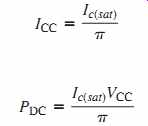
Efficiency An advantage of push-pull class B and class AB amplifiers over class A is a much higher efficiency. This advantage usually overrides the difficulty of biasing the class AB push-pull amplifier to eliminate crossover distortion. Recall that efficiency, is de fined as the ratio of ac output power to dc input power.
The maximum efficiency, for a class B amplifier (class AB is slightly less) is developed as follows, starting with EQN. 6.
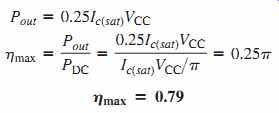
or, as a percentage,
eta max = 79%
Recall that the maximum efficiency for class A is 0.25 (25 percent).
Input Resistance
The complementary push-pull configuration used in class B/class AB amplifiers is, in effect, two emitter-followers. The input resistance for the emitter-follower, where R1 and R2 are the bias resistors, is:
Rin = Beta ac(r’ e + RE) || R1 || R2
Since RE = RL, the formula is:
Rin = Beta ac(r’ e + RL) || R1 || R2
DarlingtonClassAB Amplifier
In many applications where the push-pull configuration is used, the load resistance is relatively small. For example, an 8 ohm speaker is a common load for a class AB push-pull amplifier.
As you saw in the previous example, push-pull amplifiers can present a quite low input resistance to the preceding amplifier that drives it. Depending on the output resistance of the preceding amplifier, the low push-pull input resistance can load it severely and significantly reduce the voltage gain. As an example, if each bias resistor is 1k and if the complementary transistors in a push-pull amplifier exhibit an ac beta of 50 and the load resistance is 8 ohm, the input resistance is (assuming r’ e = 1 ohm) is:
If the collector resistance of the driving amplifier is, for example, the input resistance of the push-pull amplifier reduces the effective collector resistance of the driving amplifier (assuming a common-emitter) to Rc = RC || Rin = 1.0 k || 236 ohm= 190 ohm.
This drastically reduces the voltage gain of the driving amplifier because its gain is Rc/r’ e.
In certain applications with low-resistance loads, a push-pull amplifier using Darlington transistors can be used to increase the input resistance presented to the driving amplifier and avoid severely reducing the voltage gain. The overall ac beta of a Darlington pair is generally in excess of a thousand. Also, the bias resistors can be greater because less base current is required.
In the previous case, for example, if for each transistor in a Darlington pair, the overall ac beta is [...]
If the bias resistors are the input resistance is greatly increased, as the following calculation shows.

A Darlington class AB push-pull amplifier is shown in FIG. 19. Four diodes are required in the bias circuit to match the four base-emitter junctions of the two Darlington pairs.
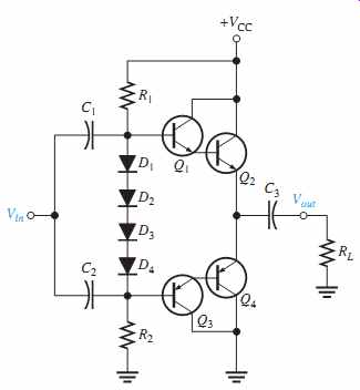
FIG. 19 A Darlington class AB push-pull amplifier.
Darlington/Complementary Darlington Class AB Amplifier
The complementary Darlington, also known as the Sziklai pair, was introduced in Section 6.
Recall that it is similar to the traditional Darlington pair except it uses complementary transistors (one npn and one pnp). The complementary Darlington is used when it is deter mined that output power transistors of the same type should be used (both npn or both pnp). FIG. 20 shows a class AB push-pull amplifier with two npn output power transistors (Q2 and Q4). The upper part of the push-pull configuration is a traditional Darlington, and the lower part is a complementary Darlington.
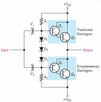
FIG. 20 A Darlington/complementary Darlington class AB push-pull amplifier.
----------
SECTION 2 CHECKUP
1. Where is the Q-point for a class B amplifier?
2. What causes crossover distortion?
3. What is the maximum efficiency of a push-pull class B amplifier?
4. Explain the purpose of the push-pull configuration for class B.
5. How does a class AB differ from a class B amplifier?
---------
