AMAZON multi-meters discounts AMAZON oscilloscope discounts
OUTLINE
1. The DC Operating Point
2. Voltage-Divider Bias
3. Other Bias Methods
4. Troubleshooting
Application Activity
Green-Tech Application 5: Wind Power
OBJECTIVES
-- Discuss and determine the dc operating point of a linear amplifier
-- Analyze a voltage-divider biased circuit
-- Analyze an emitter bias circuit, a base bias circuit, an emitter-feedback bias circuit, and a collector-feedback bias circuit
-- Troubleshoot faults in transistor bias circuits
TERMINOLOGY:
-- Q-point
-- DC load line
-- Linear region
-- Stiff voltage divider
-- Feedback
INTRODUCTION
As you learned in Section 4, a transistor must be properly biased in order to operate as an amplifier. DC biasing is used to establish fixed dc values for the transistor currents and voltages called the dc operating point or quiescent point (Q-point). In this Section, several types of bias circuits are discussed. This material lays the groundwork for the study of amplifiers, and other circuits that require proper biasing.
APPLICATION ACTIVITY PREVIEW
The Application Activity focuses on a system for controlling temperature in an industrial chemical process. You will be dealing with a circuit that converts a temperature measurement to a proportional voltage that is used to adjust the temperature of a liquid in a storage tank. The first step is to learn all you can about transistor operation. You will then apply your knowledge to the Application Activity at the end of the Section.
1. THE DC OPERATING POINT
A transistor must be properly biased with a dc voltage in order to operate as a linear amplifier. A dc operating point must be set so that signal variations at the input terminal are amplified and accurately reproduced at the output terminal. As you learned in Section 4, when you bias a transistor, you establish the dc voltage and current values.
This means, for example, that at the dc operating point, IC and VCE have specified values. The dc operating point is often referred to as the Q-point (quiescent point).
After completing this section, you should be able to:
-- Discuss and determine the dc operating point of a linear amplifier
-- Explain the purpose of dc bias
-- Define Q-point and describe how it affects the output of an amplifier
-- Explain how collector characteristic curves are produced
-- Describe and draw a dc load line
-- State the conditions for linear operation
-- Explain what causes waveform distortion
DC Bias
Bias establishes the dc operating point (Q-point) for proper linear operation of an amplifier. If an amplifier is not biased with correct dc voltages on the input and output, it can go into saturation or cutoff when an input signal is applied. FIG. 1 shows the effects of proper and improper dc biasing of an inverting amplifier. In part (a), the output signal is an amplified replica of the input signal except that it is inverted, which means that it is 180° out of phase with the input. The output signal swings equally above and below the dc bias level of the output, VDC(out). Improper biasing can cause distortion in the output signal, as illustrated in parts (b) and (c). Part (b) illustrates limiting of the positive portion of the out put voltage as a result of a Q-point (dc operating point) being too close to cutoff. Part (c) shows limiting of the negative portion of the output voltage as a result of a dc operating point being too close to saturation.
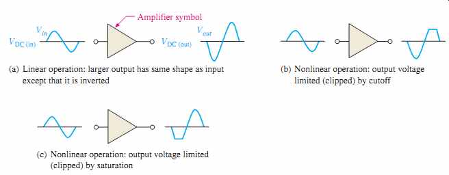
FIG. 1 Examples of linear and nonlinear operation of an inverting amplifier
(the triangle symbol). --- (a) (b) Linear operation: larger output has
same shape as input except that it is inverted Nonlinear operation: output
voltage limited (clipped) by cutoff ; (c) Nonlinear operation: output voltage
limited (clipped) by saturation
Graphical Analysis
The transistor in FIG. 2(a) is biased with VCC and VBB to obtain certain values of IB, IC, IE, and VCE. The collector characteristic curves for this particular transistor are shown in FIG. 2(b); we will use these curves to graphically illustrate the effects of dc bias.
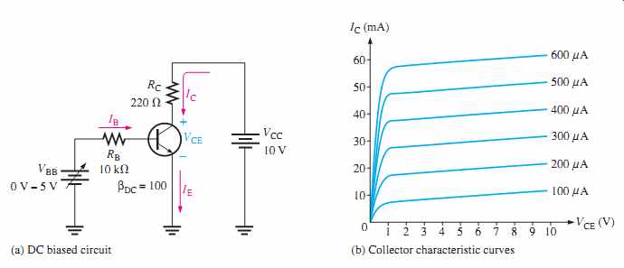
FIG. 2 A dc-biased transistor circuit with variable bias voltage (VBB)
for generating the collector characteristic curves shown in part (b).
------------
FYI
In 1965, a single transistor cost more than a dollar. By 1975, the cost of a transistor had dropped to less than a penny, while transistor size allowed for almost 100,000 transistors on a single chip. From 1979 to 1999, processor performance went from about 1.5 million instructions per second (MIPS) to over 1,000 MIPS. Today's processors, some topping out at well above one billion transistors, run at 3.2 GHz and higher, deliver over 10,000 MIPS, and can be manufactured in high volumes with transistors that cost less than 1/10,000th of a cent.
-------------
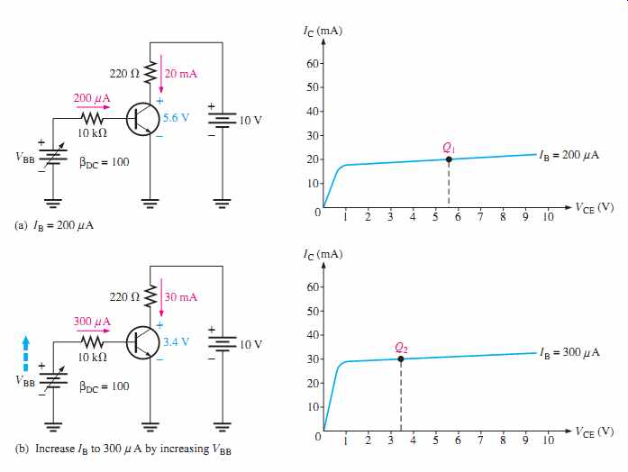
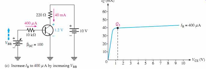
In FIG. 3, we assign three values to IB and observe what happens to IC and VCE.
First, VBB is adjusted to produce an IB of 200 uA as shown in FIG. 3(a). Since IC = beta_DC I_B the collector current is 20 mA, as indicated, and
VCE = VCC - ICRC = 10 V - (20 mA)(220 OHM) = 10 V - 4.4 V = 5.6 V
This Q-point is shown on the graph of FIG. 3(a) as Q1.
Next, as shown in FIG. 3(b), V_BB is increased to produce an IB of 300 uA and an IC of 30 mA.
VCE = 10 V - (30 mA)(220 OHM) = 10 V - 6.6 V = 3.4 V
The Q-point for this condition is indicated by Q2 on the graph.
Finally, as in FIG. 3(c), VBB is increased to give an IB of 400 uA and an IC of 40 mA.
VCE = 10 V - (40 mA)(220 OHM) = 10 V - 8.8 V = 1.2 V
Q3 is the corresponding Q-point on the graph.
DC Load Line
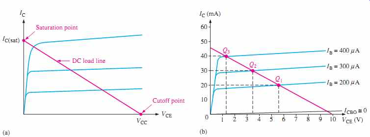
The dc operation of a transistor circuit can be described graphically using a dc load line. This is a straight line drawn on the characteristic curves from the saturation value where IC IC(sat) on the y-axis to the cutoff value where VCE VCC on the x-axis, as shown in FIG. 4(a). The load line is determined by the external circuit (VCC and RC), not the transistor itself, which is described by the characteristic curves.
In FIG. 3, the equation for IC is:
This is the equation of a straight line with a slope of -1/RC, an x intercept of VCE=VCC, and a y intercept of VCC/RC, which is I_C(sat). >
------------
FYI
Gordon Moore, one of the founders of Intel, observed in an article in the April, 1965, issue of Electronics magazine that innovations in technology would allow a doubling of the number of transistors in a given space every year (in an update article in 1975, Moore adjusted the rate to every two years to account for the growing complexity of chips), and that the speed of those transistors would increase. This prediction has become widely known as Moore's law.
------------
The point at which the load line intersects a characteristic curve represents the Q-point for that particular value of IB. FIG. 4(b) illustrates the Q-point on the load line for each value of IB in FIG. 3.
Linear Operation
The region along the load line including all points between saturation and cutoff is generally known as the linear region of the transistor's operation. As long as the transistor is operated in this region, the output voltage is ideally a linear reproduction of the input.
FIG. 5 shows an example of the linear operation of a transistor. AC quantities are indicated by lowercase italic subscripts. Assume a sinusoidal voltage, Vin, is superimposed on VBB, causing the base current to vary sinusoidally above 100 uA and below its Q-point value of 300 uA.
This, in turn, causes the collector current to vary 10 mA above and below its Q-point value of 30 mA. As a result of the variation in collector current, the collector to-emitter voltage varies 2.2 V above and below its Q-point value of 3.4 V. Point A on the load line in FIG. 5 corresponds to the positive peak of the sinusoidal input voltage.
Point B corresponds to the negative peak, and point Q corresponds to the zero value of the sine wave, as indicated. VCEQ, ICQ, and IBQ are dc Q-point values with no input sinusoidal voltage applied.
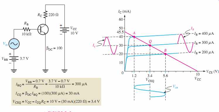
FIG. 5 Variations in collector current and collector-to-emitter voltage
as a result of a variation in base current.
Waveform Distortion
As previously mentioned, under certain input signal conditions the location of the Q-point on the load line can cause one peak of the Vce waveform to be limited or clipped, as shown in parts (a) and (b) of FIG. 6. In each case the input signal is too large for the Q-point location and is driving the transistor into cutoff or saturation during a portion of the input cycle. When both peaks are limited as in FIG. 6(c), the transistor is being driven into both saturation and cutoff by an excessively large input signal. When only the positive peak is limited, the transistor is being driven into cutoff but not saturation. When only the negative peak is limited, the transistor is being driven into saturation but not cutoff.
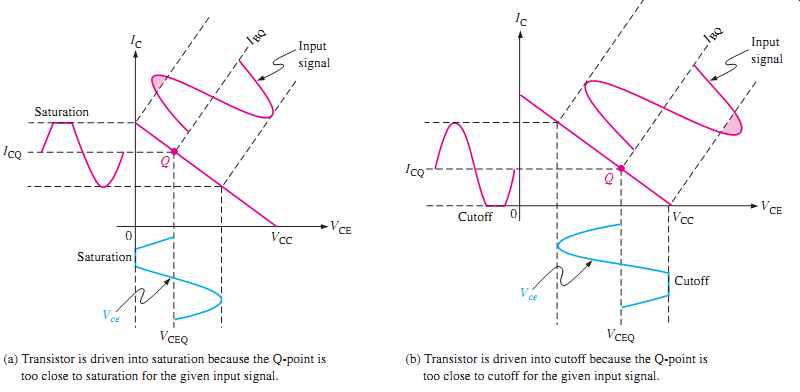
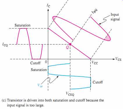
FIG. 6 Graphical load line illustration of a transistor being driven into
saturation and/or cutoff.
(a) Transistor is driven into saturation because the Q-point is too close to saturation for the given input signal.
(b) Transistor is driven into cutoff because the Q-point is too close to cutoff for the given input signal.
(c) Transistor is driven into both saturation and cutoff because the input signal is too large.
SECTION 1 CHECKUP
1. What are the upper and lower limits on a dc load line in terms of VCE and IC?
2. Define Q-point.
3. At what point on the load line does saturation occur? At what point does cutoff occur?
4. For maximum Vce, where should the Q-point be placed?
2. VOLTAGE-DIVIDER BIAS
You will now study a method of biasing a transistor for linear operation using a single source resistive voltage divider. This is the most widely used biasing method. Four other methods are covered in Section 3.
After completing this section, you should be able to:
-- Analyze a voltage-divider biased circuit
-- Define the term stiff voltage-divider
-- Calculate currents and voltages in a voltage-divider biased circuit
-- Explain the loading effects in voltage-divider bias
-- Describe how dc input resistance at the transistor base affects the bias
-- Apply Thevenin's theorem to the analysis of voltage-divider bias
-- Analyze both npn and pnp circuits
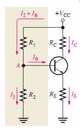
Up to this point a separate dc source, VBB, was used to bias the base-emitter junction be cause it could be varied independently of VCC and it helped to illustrate transistor operation. A more practical bias method is to use VCC as the single bias source, as shown in FIG. 9. To simplify the schematic, the battery symbol is omitted and replaced by a line termination circle with a voltage indicator (VCC) as shown.
A dc bias voltage at the base of the transistor can be developed by a resistive voltage divider that consists of R1 and R2, as shown in FIG. 9. VCC is the dc collector supply voltage. Two current paths are between point A and ground: one through R2 and the other through the base-emitter junction of the transistor and RE.
Generally, voltage-divider bias circuits are designed so that the base current is much smaller than the current (I2) through R2 in FIG. 9. In this case, the voltage-divider circuit is very straightforward to analyze because the loading effect of the base current can be ignored. A voltage divider in which the base current is small compared to the current in R2 is said to be a stiff voltage divider because the base voltage is relatively independent of different transistors and temperature effects.
To analyze a voltage-divider circuit in which IB is small compared to I2, first calculate the voltage on the base using the unloaded voltage-divider rule:
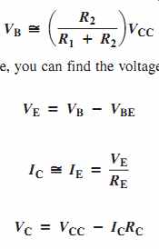
EQN. 1
EQN. 2
EQN. 3
EQN. 4
Once you know VC and VE, you can determine VCE.
VCE = VC - VE
The basic analysis developed in Example 2 is all that is needed for most voltage divider circuits, but there may be cases where you need to analyze the circuit with more ac curacy. Ideally, a voltage-divider circuit is stiff, which means that the transistor does not appear as a significant load. All circuit design involves trade-offs; and one trade-off is that stiff voltage dividers require smaller resistors, which are not always desirable because of potential loading effects on other circuits and added power requirements. If the circuit designer wanted to raise the input resistance, the divider string may not be stiff; and more detailed analysis is required to calculate circuit parameters. To determine if the divider is stiff, you need to examine the dc input resistance looking in at the base as shown in FIG. 11.
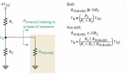
FIG. 11 Voltage divider with load.
Loading Effects of Voltage-Divider Bias
DC Input Resistance at the Transistor Base
The dc input resistance of the transistor is proportional to so it will change for different transistors. When a transistor is operating in its linear region, the emitter current (IE) is
When the emitter resistor is viewed from the base circuit, the resistor appears to be larger than its actual value because of the dc current gain in the transistor. That is, RIN(BASE) = VB/IB = VB / (IE / beta_DC).
This is the effective load on the voltage divider illustrated in FIG. 11.
You can quickly estimate the loading effect by comparing RIN(BASE) to the resistor R2 in the voltage divider. As long as RIN(BASE) is at least ten times larger than R2, the loading effect will be 10% or less and the voltage divider is stiff. If RIN(BASE) is less than ten times R2, it should be combined in parallel with R2.
Thevenin's Theorem Applied to Voltage-Divider Bias
To analyze a voltage-divider biased transistor circuit for base current loading effects, we will apply Thevenin's theorem to evaluate the circuit. First, let's get an equivalent base emitter circuit for the circuit in FIG. 13(a) using Thevenin's theorem. Looking out from the base terminal, the bias circuit can be redrawn as shown in FIG. 13(b). Apply Thevenin's theorem to the circuit left of point A, with VCC replaced by a short to ground and the transistor disconnected from the circuit. The voltage at point A with respect to ground is
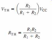
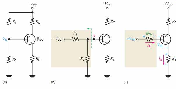
FIG. 13 Thevenizing the bias circuit.
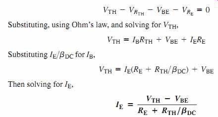
The Thevenin equivalent of the bias circuit, connected to the transistor base, is shown in the beige box in FIG. 13(c). Applying Kirchhoff's voltage law around the equivalent base-emitter loop gives
If is small compared to RE, the result is the same as for an unloaded voltage divider.
Voltage-divider bias is widely used because reasonably good bias stability is achieved with a single supply voltage.
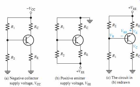
FIG. 14 Voltage-divider biased pnp transistor.
(a) Negative collector supply voltage, VCC (b) Positive emitter supply voltage, VEE (c) The circuit in (b) redrawn
Voltage-Divider Biased PNP Transistor
As you know, a pnp transistor requires bias polarities opposite to the npn. This can be accomplished with a negative collector supply voltage, as in FIG. 14(a), or with a positive emitter supply voltage, as in FIG. 14(b).
RTH > beta_DC
In a schematic, the pnp is often drawn upside down so that the supply voltage is at the top of the schematic and ground at the bottom, as in FIG. 14(c).
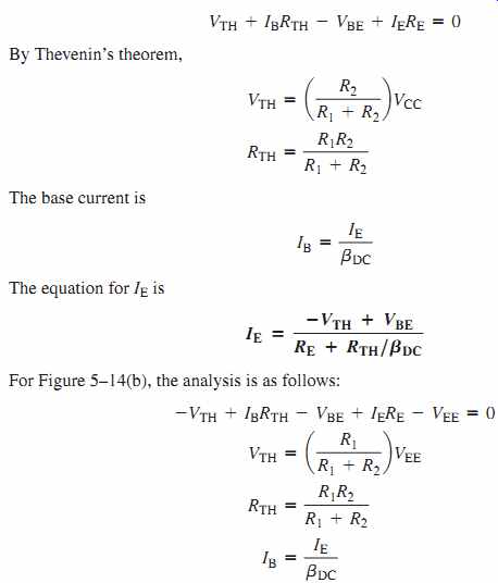
The analysis procedure is the same as for an npn transistor circuit using Thevenin's theorem and Kirchhoff's voltage law, as demonstrated in the following steps with reference to FIG. 14. For FIG. 14(a), applying Kirchhoff's voltage law around the base-emitter circuit gives

EQN. 8
SECTION 2 CHECKUP
1. If the voltage at the base of a transistor is 5 V and the base current is A, what is the dc input resistance at the base?
2. If a transistor has a dc beta of 190, VB=2 V, and IE=2 mA, what is the dc input resistance at the base?
3. What bias voltage is developed at the base of a transistor if both resistors in a stiff voltage divider are equal and VCC = +10 V?
4. What are two advantages of voltage-divider bias?
3. OTHER BIAS METHODS
In this section, four additional methods for dc biasing a transistor circuit are discussed.
Although these methods are not as common as voltage-divider bias, you should be able to recognize them when you see them and understand the basic differences.
After completing this section, you should be able to:
-- Analyze four more types of bias circuits
-- Discuss emitter bias
-- Analyze an emitter-biased circuit
-- Discuss base bias
-- Analyze a base-biased circuit
-- Explain Q-point stability of base bias
-- Discuss emitter-feedback bias
-- Define negative feedback
-- Analyze an emitter-feedback biased circuit
-- Discuss collector-feedback bias
-- Analyze a collector-feedback biased circuit
-- Discuss Q-point stability over temperature
Emitter Bias
Emitter bias provides excellent bias stability in spite of changes in or temperature. It uses both a positive and a negative supply voltage. To obtain a reasonable estimate of the key dc values in an emitter-biased circuit, analysis is quite easy. In an npn circuit, such as shown b in FIG. 17, the small base current causes the base voltage to be slightly below ground.
The emitter voltage is one diode drop less than this. The combination of this small drop across RB and VBE forces the emitter to be at approximately -1V.
Using this approximation, you can obtain the emitter current as:
V_EE is entered as a negative value in this equation.
You can apply the approximation that to calculate the collector voltage.
IC _ IE RE
The approximation that VE=-1V is useful for troubleshooting because you won't need to perform any detailed calculations. As in the case of voltage-divider bias, there is a more rigorous calculation for cases where you need a more exact result.
VC = V_CC – I_C R_C
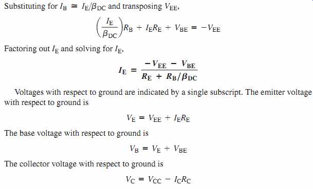
The approximation that VE = -1V and the neglect of beta_DC may not be accurate enough for design work or detailed analysis. In this case, Kirchhoff's voltage law can be applied as follows to develop a more detailed formula for IE. Kirchhoff's voltage law applied around the base-emitter circuit in FIG. 17(a), which has been redrawn in part (b) for analysis, gives the following equation:
VEE + IBRB + VBE + IERE = 0
Substituting, using Ohm's law,
VEE + VRB + VBE + VRE = 0
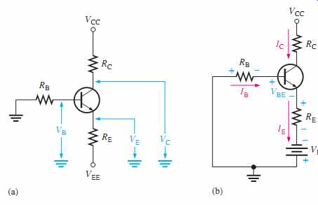
FIG. 17 An npn transistor with emitter bias.
Polarities are reversed for a pnp transistor. Single subscripts indicate volt ages with respect to ground.
Base Bias
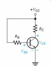
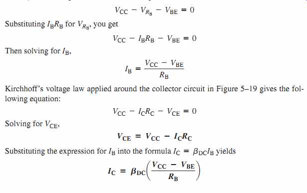
This method of biasing is common in switching circuits. FIG. 19 shows a base-biased transistor. The analysis of this circuit for the linear region shows that it is directly depend ent on Starting with Kirchhoff's voltage law around the base circuit, bDC.
EQN. 11
Q-Point Stability of Base Bias
Notice that EQN. 11 shows that IC is dependent on beta_DC. The disadvantage of this is that a variation in bDC causes IC and, as a result, VCE to change, thus changing the Q-point of the transistor. This makes the base bias circuit extremely beta-dependent and unpredictable.
Recall that bDC varies with temperature and collector current. In addition, there is a large spread of b_DC values from one transistor to another of the same type due to manufacturing variations. For these reasons, base bias is rarely used in linear circuits but is discussed here so you will be familiar with it.
Emitter-Feedback Bias
If an emitter resistor is added to the base-bias circuit in FIG. 20, the result is emitter feedback bias, as shown in FIG. 21. The idea is to help make base bias more predictable with negative feedback, which negates any attempted change in collector current with an opposing change in base voltage. If the collector current tries to increase, the emitter voltage increases, causing an increase in base voltage because VB=VE + VBE. This in crease in base voltage reduces the voltage across RB, thus reducing the base current and keeping the collector current from increasing. A similar action occurs if the collector cur rent tries to decrease. While this is better for linear circuits than base bias, it is still dependent on beta_DC and is not as predictable as voltage-divider bias. To calculate IE, you can write Kirchhoff's voltage law (KVL) around the base circuit.
-VCC + IB RB + VBE + IE RE = 0
Substituting IE/b_DC for IB, you can see that IE is still dependent on bDC:
IE = VCC - VBE / [(R_E + R_B/beta_DC)]
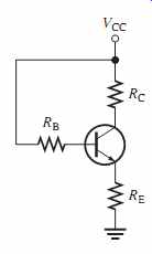
FIG. 21 Emitter-feedback bias.
Collector-Feedback Bias
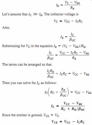
In FIG. 22, the base resistor RB is connected to the collector rather than to VCC, as it was in the base bias arrangement discussed earlier. The collector voltage provides the bias for the base-emitter junction. The negative feedback creates an "offsetting" effect that tends to keep the Q-point stable. If IC tries to increase, it drops more voltage across RC, thereby causing VC to decrease. When VC decreases, there is a decrease in voltage across RB, which decreases IB. The decrease in IB produces less IC which, in turn, drops less volt age across RC and thus offsets the decrease in VC.
Analysis of a Collector-Feedback Bias Circuit
By Ohm's law, the base current can be expressed as:
EQN. 14
Q-Point Stability Over Temperature
EQN. 13 shows that the collector current is dependent to some extent on bDC and VBE. This dependency, of course, can be minimized by making RC >> RB/bDC and VCC >> VBE.
An important feature of collector-feedback bias is that it essentially eliminates the bDC dependency even if the stated conditions are met.
As you have learned, bDC varies directly with temperature, and VBE varies inversely with temperature. As the temperature goes up in a collector-feedback circuit, bDC goes up and VBE goes down. The increase in bDC acts to increase I_C. The decrease in VBE acts to increase IB which, in turn also acts to increase IC. As IC tries to increase, the voltage drop across RC also tries to increase. This tends to reduce the collector voltage and therefore the voltage across RB, thus reducing IB and offsetting the attempted increase in I_C and the attempted decrease in VC. The result is that the collector-feedback circuit maintains a relatively stable Q-point. The reverse action occurs when the temperature decreases.
SECTION 3 CHECKUP
1. Why is emitter bias more stable than base bias?
2. What is the main disadvantage of emitter bias?
3. Explain how an increase in causes a reduction in base current in a collector-feed back circuit.
4. What is the main disadvantage of the base bias method?
5. Explain why the base bias Q-point changes with temperature.
6. How does emitter-feedback bias improve on base bias? bDC
4. TROUBLESHOOTING
In a biased transistor circuit, the transistor can fail or a resistor in the bias circuit can fail. We will examine several possibilities in this section using the voltage-divider bias arrangement. Many circuit failures result from open resistors, internally open transistor leads and junctions, or shorted junctions. Often, these failures can produce an apparent cutoff or saturation condition when voltage is measured at the collector.
After completing this section, you should be able to:
-- Troubleshoot faults in transistor bias circuits
-- Troubleshoot a voltage-divider biased transistor circuit
-- Troubleshoot the circuit for several common faults
-- Use voltage measurement to isolate a fault
Troubleshooting a Voltage-Divider Biased Transistor
An example of a transistor with voltage-divider bias is shown in FIG. 24. For the specific component values shown, you should get the voltage readings approximately as indicated when the circuit is operating properly.
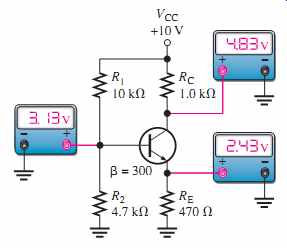
FIG. 24 A voltage-divider biased transistor with correct voltages.
For this type of bias circuit, a particular group of faults will cause the transistor collector to be at VCC when measured with respect to ground. Five faults are indicated for the circuit in FIG. 25(a). The collector voltage is equal to 10 V with respect to ground for each of the faults as indicated in the table in part (b). Also, for each of the faults, the base voltage and the emitter voltage with respect to ground are given.
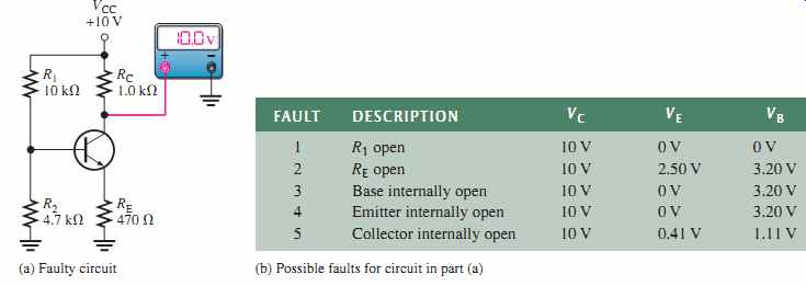
FIG. 25 Faults for which VC = VCC.
Fault 1: Resistor R1 Open
This fault removes the bias voltage from the base, thus connecting the base to ground through R2 and forcing the transistor into cutoff because VB=0 V and IB=0 A. The transistor is nonconducting so there is no IC and, therefore, no voltage drop across RC. This makes the collector voltage equal to VCC (10 V). Since there is no base cur rent or collector current, there is also no emitter current and VE 0 V.
Fault 2: Resistor RE Open
This fault prevents base current, emitter current, and collector current except for a very small ICBO that can be neglected. Since IC=0 A, there is no voltage drop across RC and, therefore, VC = VCC = 10 V. The voltage divider produces a voltage at the base with respect to ground as follows:

When a voltmeter is connected to the emitter, it provides a current path through its high internal impedance, resulting in a forward-biased base-emitter junction. Therefore, the emitter voltage is VE = VB - VBE. The amount of the forward voltage drop across the BE junction depends on the current. VBE = 0.7 V is assumed for purposes of illustration, but it may be much less. The result is an emitter voltage as follows:

Fault 3: Base Internally Open
An internal transistor fault is more likely to happen than an open resistor. Again, the transistor is nonconducting so IC = 0 A and VC = VCC = 10 V.
Just as for the case of the open RE, the voltage divider produces 3.2 V at the external base connection. The voltage at the external emitter connection is 0 V because there is no emitter current through RE and, thus, no voltage drop.
Fault 4: Emitter Internally Open
Again, the transistor is nonconducting, so IC = 0A and VC = VCC = 10 V. Just as for the case of the open RE and the internally open base, the voltage divider produces 3.2 V at the base. The voltage at the external emitter lead is 0 V because that point is open and connected to ground through RE. Notice that Faults 3 and 4 produce identical symptoms.
Fault 5: Collector InternallyOpen
Since there is an internal open in the transistor collector, there is no IC and, therefore, VC= VCC=10 V. In this situation, the voltage divider is loaded by RE through the forward-biased BE junction, as shown by the approximate equivalent circuit in FIG. 26. The base voltage and emitter voltage are determined as follows:

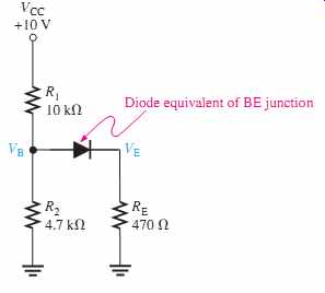
FIG. 26 Equivalent bias circuit for an internally open collector.
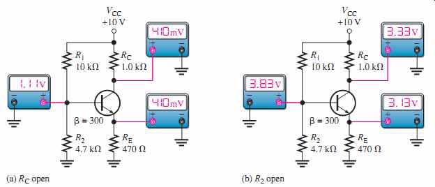
FIG. 27 Faults for which the transistor is conducting or appears to be
conducting.
There are two possible additional faults for which the transistor is conducting or appears to be conducting, based on the collector voltage measurement. These are indicated in FIG. 27.
Fault 6: Resistor RC Open
For this fault, which is illustrated in FIG. 27(a), the collector voltage may lead you to think that the transistor is in saturation, but actually it is nonconducting. Obviously, if RC is open, there can be no collector current. In this situation, the equivalent bias circuit is the same as for Fault 5, as illustrated in FIG. 26.
Therefore, VB = 1.11 V and since the BE junction is forward-biased, VC = VB - VBC = 1.11 V - 0.7 V = 0.41 V
When a voltmeter is connected to the collector to measure VC, a current path is provided through the internal impedance of the meter and the BC junction is forward-biased by VB.
Therefore, VE = VB - VBE = 1.11 V - 0.7 V = 0.41 V
Again the forward drops across the internal transistor junctions depend on the current.
We are using 0.7 V for illustration, but the forward drops may be much less.
Fault 7: Resistor R2 Open
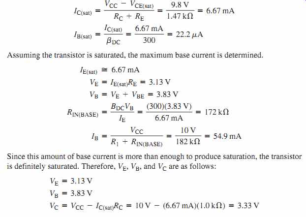
When R2 opens as shown in FIG. 27(b), the base voltage and base current increase from their normal values because the voltage divider is now formed by and In this case, the base voltage is determined by the emitter voltage (VB = VE + VBE).
First, verify whether the transistor is in saturation or not. The collector saturation cur rent and the base current required to produce saturation are determined as follows (assuming VCE(sat) =0.2 V):
SECTION 4 CHECKUP
1. How do you determine when a transistor is saturated? When a transistor is in cutoff?
2. In a voltage-divider biased npn transistor circuit, you measure VCC at the collector and an emitter voltage 0.7 V less than the base voltage. Is the transistor functioning in cut off, or is RE open?
3. What symptoms does an open R produce?
-------------------
---------

