AMAZON multi-meters discounts AMAZON oscilloscope discounts
<< cont. from part 1
3. THE CLASS C AMPLIFIER
Class C amplifiers are biased so that conduction occurs for much less than 180°.
Class C amplifiers are more efficient than either class A or push-pull class B and class AB, which means that more output power can be obtained from class C operation. The output amplitude is a nonlinear function of the input, so class C amplifiers are not used for linear amplification. They are generally used in radio frequency (RF) applications, including circuits, such as oscillators, that have a constant output amplitude, and modulators, where a high-frequency signal is controlled by a low-frequency signal.
Goals:
-- Explain and analyze the operation of class C amplifiers
-- Describe basic class C operation
-- Discuss the bias of the transistor
-- Discuss class C power dissipation
-- Explain tuned operation
-- Determine maximum output power
-- Explain clamper bias for a class C amplifier
-----------

FIG. 21 Basic class C amplifier operation (noninverting).
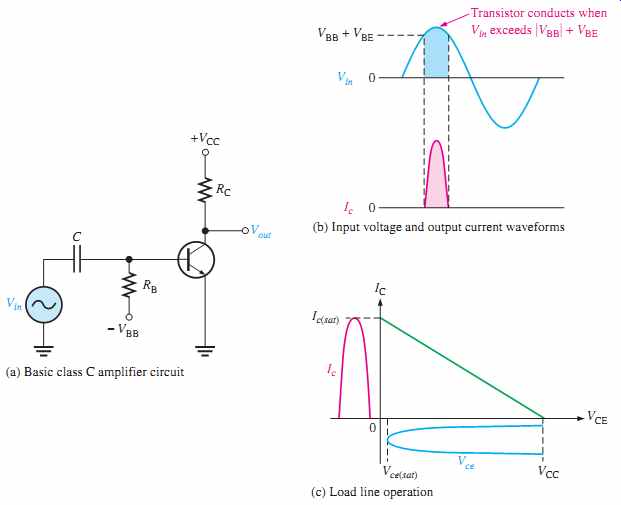
FIG. 22 Basic class C operation.
------------
Basic Class C Operation
The basic concept of class C operation is illustrated in FIG. 21. A common-emitter class C amplifier with a resistive load is shown in FIG. 22(a). A class C amplifier is normally operated with a resonant circuit load, so the resistive load is used only for the purpose of illustrating the concept. It is biased below cutoff with the negative VBB supply.
The ac source voltage has a peak value that is slightly greater than |VBB| + VBE
so that the base voltage exceeds the barrier potential of the base-emitter junction for a short time near the positive peak of each cycle, as illustrated in FIG. 22(b). During this short interval, the transistor is turned on. When the entire ac load line is used, as shown in FIG. 22(c), the ideal maximum collector current is Ic(sat), and the ideal minimum collector voltage is Vce(sat).
Power Dissipation
The power dissipation of the transistor in a class C amplifier is low because it is on for only a small percentage of the input cycle. FIG. 23(a) shows the collector current pulses.
The time between the pulses is the period (T ) of the ac input voltage. The collector current and the collector voltage during the on time of the transistor are shown in FIG. 23(b).
To avoid complex mathematics, we will assume ideal pulse approximations. Using this simplification, if the output swings over the entire load, the maximum current amplitude is Ic(sat) and the minimum voltage amplitude is Vce(sat) during the time the transistor is on.
The power dissipation during the on time is, therefore,
PD(on) = Ic (sat)Vce (sat)
The transistor is on for a short time, ton, and off for the rest of the input cycle. Therefore, assuming the entire load line is used, the power dissipation averaged over the entire cycle is


FIG.
23 Class C waveforms. (a) Collector current pulses (b) Ideal class C waveforms
Tuned Operation
Because the collector voltage (output) is not a replica of the input, the resistively loaded class C amplifier alone is of no value in linear applications. It is therefore necessary to use a class C amplifier with a parallel resonant circuit (tank), as shown in FIG. 24(a). The resonant frequency of the tank circuit is determined by the formula fr = 1/(2 pi radic.(LC)).
The short pulse of collector current on each cycle of the input initiates and sustains the oscillation of the tank circuit so that an output sinusoidal voltage is produced, as illustrated in FIG. 24(b). The tank circuit has high impedance only near the resonant frequency, so the gain is large only at this frequency.
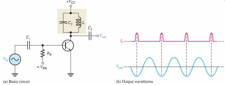
FIG. 24 Tuned class C amplifier.
The current pulse charges the capacitor to approximately +VCC, as shown in FIG. 25(a). After the pulse, the capacitor quickly discharges, thus charging the inductor.
Then, after the capacitor completely discharges, the inductor's magnetic field collapses and then quickly recharges C to near VCC in a direction opposite to the previous charge.
This completes one half-cycle of the oscillation, as shown in parts (b) and (c) of FIG. 25. Next, the capacitor discharges again, increasing the inductor's magnetic field.
The inductor then quickly recharges the capacitor back to a positive peak slightly less than the previous one, due to energy loss in the winding resistance. This completes one full cycle, as shown in parts (d) and (e) of FIG. 25. The peak-to-peak output voltage is therefore approximately equal to 2VCC.
The amplitude of each successive cycle of the oscillation will be less than that of the previous cycle because of energy loss in the resistance of the tank circuit, as shown in FIG. 26(a), and the oscillation will eventually die out. However, the regular recurrences of the collector current pulse re-energizes the resonant circuit and sustains the oscillations at a constant amplitude.
When the tank circuit is tuned to the frequency of the input signal (fundamental), re energizing occurs on each cycle of the tank voltage, Vr , as shown in FIG. 26(b). When the tank circuit is tuned to the second harmonic of the input signal, re-energizing occurs on alternate cycles as shown in FIG. 26(c). In this case, a class C amplifier operates as a frequency multiplier (x 2). By tuning the resonant tank circuit to higher harmonics, further frequency multiplication factors are achieved.
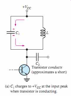
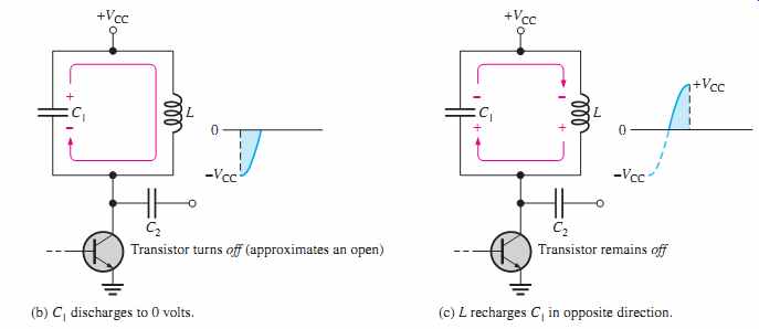
FIG. 25 Resonant circuit action.
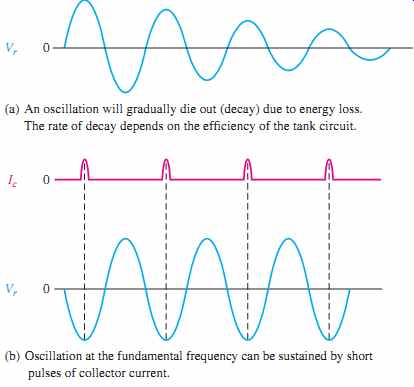
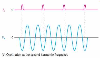
FIG. 26 Tank circuit oscillations. Vr is the voltage across the tank
circuit.
Maximum Output Power
Since the voltage developed across the tank circuit has a peak-to-peak value of approximately 2VCC, the maximum output power can be expressed as:
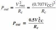
[Eqn. 9]
Rc is the equivalent parallel resistance of the collector tank circuit at resonance and represents the parallel combination of the coil resistance and the load resistance. It usually has a low value. The total power that must be supplied to the amplifier is:
Therefore, the efficiency is:

When the class C efficiency closely approaches 1 (100 percent).
[ EQN. 10]
Clamper Bias for a Class C Amplifier
FIG. 27 shows a class C amplifier with a base bias clamping circuit. The base-emitter junction functions as a diode.
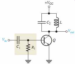
FIG. 27 Tuned class C amplifier with clamper bias.
When the input signal goes positive, capacitor C1 is charged to the peak value with the polarity shown in FIG. 28(a). This action produces an average voltage at the base of approximately -Vp.
This places the transistor in cutoff except at the positive peaks, when the transistor conducts for a short interval. For good clamping action, the R1C1 time constant of the clamping circuit must be much greater than the period of the input signal. Parts (b) through (f) of FIG. 28 illustrate the bias clamping action in more detail. During the time up to the positive peak of the input (t0 to t1), the capacitor charges to Vp - 0.7 V through the base-emitter diode, as shown in part (b). During the time from t1 to t2, as shown in part (c), the capacitor discharges very little because of the large RC time constant. The capacitor, therefore, maintains an average charge slightly less than Vp - 0.7 V.
Since the dc value of the input signal is zero (positive side of C1), the dc voltage at the base (negative side of C1) is slightly more positive than -(Vp - 0.7 V), as indicated in FIG. 28(d). As shown in FIG. 28(e), the capacitor couples the ac input signal through to the base so that the voltage at the transistor's base is the ac signal riding on a dc level slightly more positive than -(Vp - 0.7 V).
Near the positive peaks of the input volt age, the base voltage goes slightly above 0.7 V and causes the transistor to conduct for a short time, as shown in FIG. 28(f).
----------
SECTION 3 CHECKUP
1. At what point is a class C amplifier normally biased?
2. What is the purpose of the tuned circuit in a class C amplifier?
3. A certain class C amplifier has a power dissipation of 100 mW and an output power of 1 W. What is its percent efficiency?
----------
----------
4. TROUBLESHOOTING
In this section, examples of isolating a component failure in a circuit are presented.
We will use a class A amplifier and a class AB amplifier with the output voltage monitored by an oscilloscope. Several incorrect output waveforms will be examined and the most likely faults will be discussed.
After completing this section, you should be able to
-- Troubleshoot power amplifiers
-- Troubleshoot a class A amplifier for various faults
-- Troubleshoot a class AB amplifier for various faults
-------
Case 1: Class A
As shown in FIG. 30, the class A power amplifier should have a normal sinusoidal out put when a sinusoidal input signal is applied.
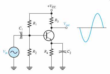
FIG. 30 Class A power amplifier with correct output voltage swing.
Now let's consider four incorrect output waveforms and the most likely causes in each case. In FIG. 31(a), the scope displays a dc level equal to the dc supply voltage, indicating that the transistor is in cutoff. The two most likely causes of this condition are (1) the transistor has an open pn junction, or (2) R4 is open, preventing collector and emitter current.

FIG. 31 Oscilloscope displays showing output voltage for the amplifier
in FIG. 30 for several types of failures. (a) Transistor in cutoff (b)
CE short or R2 open (c) Q-point shift or R1 open (d) Transistor in saturation
In FIG. 31(b), the scope displays a dc level at the collector approximately equal to the dc emitter voltage. The two probable causes of this indication are (1) the transistor is shorted from collector to emitter, or (2) R2 is open, causing the transistor to be biased in saturation. In the second case, a sufficiently large input signal can bring the transistor out of saturation on its negative peaks, resulting in short pulses on the output.
In FIG. 31(c), the scope displays an output waveform that indicates the transistor is in cutoff except during a small portion of the input cycle. Possible causes of this indication are (1) the Q-point has shifted down due to a drastic out-of-tolerance change in a resistor value, or (2) R1 is open, biasing the transistor in cutoff. The display shows that the input signal is sufficient to bring it out of cutoff for a small portion of the cycle.
In FIG. 31(d), the scope displays an output waveform that indicates the transistor is saturated except during a small portion of the input cycle. Again, it is possible that an incorrect resistance value has caused a drastic shift in the Q-point up toward saturation, or R2 is open, causing the transistor to be biased in saturation, and the input signal is bringing it out of saturation for a small portion of the cycle.
Case 2: ClassAB
As shown in FIG. 32, the class AB push-pull amplifier should have a sinusoidal output when a sinusoidal input signal is applied.
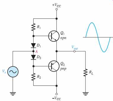
FIG. 32 A class AB push-pull amplifier with correct output voltage.
Two incorrect output waveforms are shown in FIG. 33. The waveform in part (a) shows that only the positive half of the input signal is present on the output. One possible cause is that diode D1 is open. If this is the fault, the positive half of the input signal forward biases D2 and causes transistor Q2 to conduct. Another possible cause is that the base-emitter junction of Q2 is open so only the positive half of the input signal appears on the output because Q1 is still working.
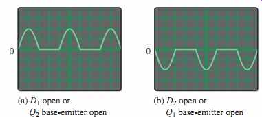
FIG. 33 Incorrect output waveforms for the amplifier in FIG. 32.
(a) D1 open or Q2 base-emitter open (b) D2 open or Q1 base-emitter open
The waveform in FIG. 33(b) shows that only the negative half of the input signal is present on the output. One possible cause is that diode D2 is open. If this is the fault, the negative half of the input signal forward-biases D1 and places the half-wave signal on the base of Q1. Another possible cause is that the base-emitter junction of Q1 is open so only the negative half of the input signal appears on the output because Q2 is still working.
------
SECTION 4 CHECKUP
1. What would you check for if you noticed clipping at both peaks of the output waveform?
2. A significant loss of gain in the amplifier of FIG. 30 would most likely be caused by what type of failure?
----------
Application Activity: The Complete PA System
The class AB power amplifier follows the audio preamp and drives the speaker as shown in the PA system block diagram in FIG. 34. In this application, the power amplifier is developed and interfaced with the preamp that was developed in Section 6. The maximum signal power to the speaker should be approximately 6 W for a frequency range of 70 Hz to 5 kHz. The dynamic range for the input voltage is up to 40 mV. Finally, the complete PA system is put together.
The Power Amplifier Circuit
The schematic of the push-pull power amplifier is shown in FIG. 35. The circuit is a class AB amplifier implemented with Darlington configurations and diode current mirror bias. Both a traditional Darlington pair and a complementary Darlington (Sziklai) pair are used to provide sufficient current to an speaker load. The signal from the preamp is 8 Ω
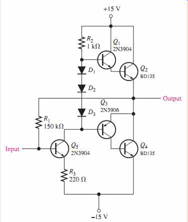
FIG. 35 Class AB power push-pull amplifier.
capacitively coupled to the driver stage, Q5, which is used to prevent excessive loading on the preamp and provide additional gain. Notice that Q5 is biased with the dc output volt age (0 V) fed back through R1. Also, the signal voltage fed back to the base of Q5 is out of-phase with the signal from the preamp and has the effect of stabilizing the gain. This is called negative feedback. The amplifier will deliver up to 5 W to an speaker.
A partial datasheet for the BD135 power transistor is shown in FIG. 36.
1. Estimate the input resistance of the power amplifier in FIG. 35.
2. Calculate the approximate voltage gain of the power amplifier in FIG. 35? 8 Ω
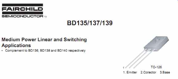
FIG. 36 Partial datasheet for the BD135 power transistors. Copyright
Fairchild semiconductor corporation.
Simulation
The power amplifier is simulated using software with a 1 kHz input signal at near its maximum linear operation. The results are shown in FIG. 37 where an 8.2 ohm resistor is used to closely approximate the 8 ohm speaker.
3. Calculate the power to the load in FIG. 37.
4. What is the measured voltage gain? The input is a peak value.
5. Compare the measured gain to the calculated gain for the amplifier in FIG. 35.
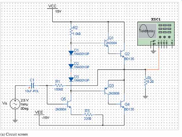
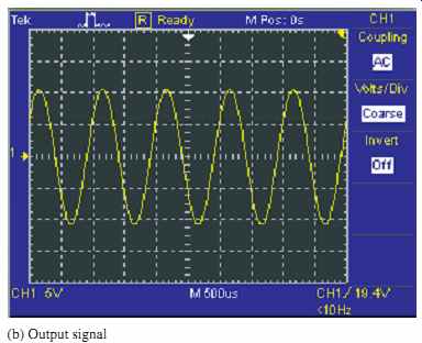
FIG. 37 Simulation of the power amplifier.
The Complete Audio Amplifier
Both the preamp and the power amp have been simulated individually. Now, they must work together to produce the required signal power to the speaker. FIG. 38 is the simulation of the combined audio preamp and power amp. Components in the power amplifier are now numbered sequentially with the preamp components.
6. Calculate the power to the load in FIG. 38.
7. What is the measured voltage gain of the power amplifier?
8. What is the measured overall voltage gain?
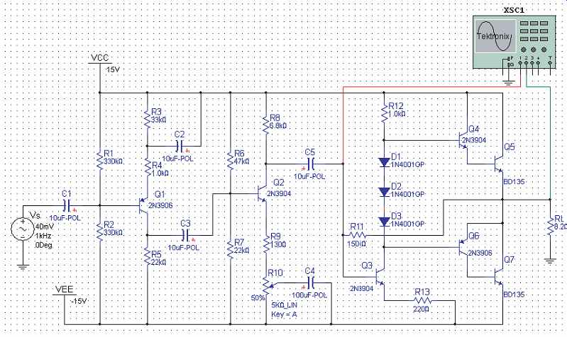
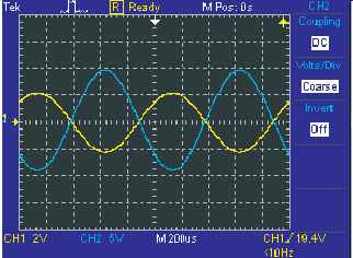
FIG. 38 Simulation of the complete audio amplifier.
Simulate the audio amplifier using software. Observe the operation with the virtual oscilloscope.
Prototyping and Testing
Now that the circuit has been simulated, the prototype circuit is constructed and tested.
After the circuit is successfully tested on a protoboard, it is ready to be finalized on a printed circuit board.
Lab Experiment
Circuit Board
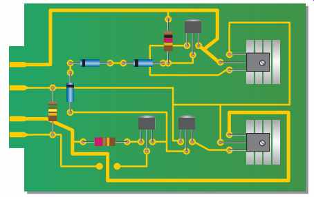
The power amplifier is implemented on a printed circuit board as shown in FIG. 39.
Heat sinks are used to provide additional heat dissipation from the power transistors.
9. Check the printed circuit board and verify that it agrees with the schematic in FIG. 35. The volume control potentiometer is mounted off the PC board for easy access.
10. Label each input and output pin according to function. Locate the single back side trace.
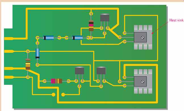
FIG. 39 Power amplifier circuit board.
Troubleshooting the Power Amplifier Board A power amplifier circuit board has failed the production test. Test results are shown in FIG. 40.
11. Based on the scope displays, list possible faults for the circuit board.
Putting the System Together
The preamp circuit board and the power amplifier circuit board are interconnected and the dc power supply (battery pack), microphone, speaker, and volume control potentiometer are attached, as shown in FIG. 41.
12. Verify that the system interconnections are correct.
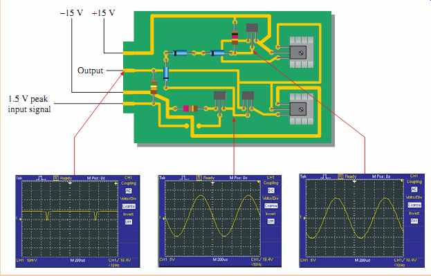
FIG. 40 Test of faulty power amplifier board.
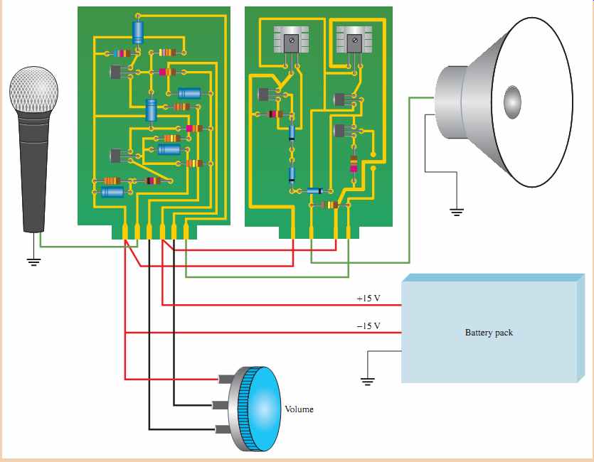
FIG. 41 The complete public address system.
SUMMARY
Section 1
-- A class A power amplifier operates entirely in the linear region of the transistor's characteristic curves. The transistor conducts during the full 360 deg. of the input cycle.
-- The Q-point must be centered on the load line for maximum class A output signal swing.
-- The maximum efficiency of a class A power amplifier is 25 percent.
Section 2
-- A class B amplifier operates in the linear region for half of the input cycle and it is in cutoff for the other half.
-- The Q-point is at cutoff for class B operation.
-- Class B amplifiers are normally operated in a push-pull configuration in order to produce an output that is a replica of the input.
-- The maximum efficiency of a class B amplifier is 79 percent.
-- A class AB amplifier is biased slightly above cutoff and operates in the linear region for slightly more than 180 deg. of the input cycle.
-- Class AB eliminates crossover distortion found in pure class B.
Section 3
- - A class C amplifier operates in the linear region for only a small part of the input cycle.
-- The class C amplifier is biased below cutoff.
-- Class C amplifiers are normally operated as tuned amplifiers to produce a sinusoidal output.
-- The maximum efficiency of a class C amplifier is higher than that of either class A or class B amplifiers. Under conditions of low power dissipation and high output power, the efficiency can approach 100 percent.
TERMINOLOGY
Class A -- A type of amplifier that operates entirely in its linear (active) region.
Class AB -- A type of amplifier that is biased into slight conduction.
Class B -- A type of amplifier that operates in the linear region for 180 deg. of the input cycle because it is biased at cutoff.
Class C --- A type of amplifier that operates only for a small portion of the input cycle.
Efficiency--The ratio of the signal power delivered to a load to the power from the power supply of an amplifier.
Power gain -- The ratio of output power to input power of an amplifier.
Push-Pull -- A type of class B amplifier with two transistors in which one transistor conducts for one half-cycle and the other conducts for the other half-cycle.
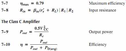
IMPORTANT FORMULAS


TRUE/FALSE QUIZ
1. Class A power amplifiers are a type of large-signal amplifier.
2. Ideally, the Q-point should be centered on the load line in a class A amplifier.
3. The quiescent power dissipation occurs when the maximum signal is applied.
4. Efficiency is the ratio of output signal power to total power.
5. Each transistor in a class B amplifier conducts for the entire input cycle.
6. Class AB operation overcomes the problem of crossover distortion.
7. Complementary symmetry transistors must be used in a class AB amplifier.
8. A current mirror is implemented with a laser diode.
9. Darlington transistors can be used to increase the input resistance of a class AB amplifier.
10. The transistor in a class C amplifier conducts for a small portion of the input cycle.
11. The output of a class C amplifier is a replica of the input signal.
12. A class C amplifier usually employs a tuned circuit.
CIRCUIT-ACTION QUIZ
1. If the value of R3 in FIG. 5 is decreased, the voltage gain of the first stage will (a) increase (b) decrease (c) not change
2. If the value of RE2 in FIG. 5 is increased, the voltage gain of the first stage will (a) increase (b) decrease (c) not change
3. If C2 in FIG. 5 opens, the dc voltage at the emitter of Q1 will (a) increase (b) decrease (c) not change
4. If the value of R4 in FIG. 5 is increased, the dc voltage at the base of Q3 will (a) increase (b) decrease (c) not change
5. If VCC in FIG. 18 is increased, the peak output voltage will (a) increase (b) decrease (c) not change
6. If the value of RL in FIG. 18 is increased, the ac output power will (a) increase (b) decrease (c) not change
7. If the value of RL in FIG. 19 is decreased, the voltage gain will (a) increase (b) decrease (c) not change
8. If the value of VCC in FIG. 19 is increased, the ac output power will (a) increase (b) decrease (c) not change
9. If the values of R1 and R2 in FIG. 19 are increased, the voltage gain will (a) increase (b) decrease (c) not change
10. If the value of C2 in FIG. 24 is decreased, the resonant frequency will (a) increase (b) decrease (c) not change
SELF-TEST
Section 1
1. An amplifier that operates in the linear region at all times is (a) Class A (b) Class AB (c) Class B (d) Class C
2. A certain class A power amplifier delivers 5 W to a load with an input signal power of 100 mW. The power gain is (a) 100 (b) 50 (c) 250 (d) 5
3. The peak current a class A power amplifier can deliver to a load depends on the (a) maximum rating of the power supply (b) quiescent current (c) current in the bias resistors (d) size of the heat sink
4. For maximum output, a class A power amplifier must maintain a value of quiescent current that is (a) one-half the peak load current (b) twice the peak load current (c) at least as large as the peak load current (d) just above the cutoff value
5. A certain class A power amplifier has
The maximum signal power output is (a) 6 W (b) 12 W (c) 1 W (d) 0.707 W
6. The efficiency of a power amplifier is the ratio of the power delivered to the load to the (a) input signal power (b) power dissipated in the last stage (c) power from the dc power supply (d) none of these answers
7. The maximum efficiency of a class A power amplifier is (a) 25% (b) 50% (c) 79% (d) 98% Section 2 8. The transistors in a class B amplifier are biased (a) into cutoff (b) in saturation (c) at midpoint of the load line (d) right at cutoff
9. Crossover distortion is a problem for (a) class A amplifiers (b) class AB amplifiers (c) class B amplifiers (d) all of these amplifiers
10. A BJT class B push-pull amplifier with no transformer coupling uses (a) two npn transistors (b) two pnp transistors (c) complementary symmetry transistors (d) none of these
11. A current mirror in a push-pull amplifier should give an ICQ that is (a) equal to the current in the bias resistors and diodes (b) twice the current in the bias resistors and diodes (c) half the current in the bias resistors and diodes (d) zero
12. The maximum efficiency of a class B push-pull amplifier is (a) 25% (b) 50% (c) 79% (d) 98%
13. The output of a certain two-supply class B push-pull amplifier has a VCC of 20 V. If the load resistance is the value of Ic(sat) is (a) 5 mA (b) 0.4 A (c) 4 mA (d) 40 mA
14. The maximum efficiency of a class AB amplifier is (a) higher than a class B (b) the same as a class B (c) about the same as a class A (d) slightly less than a class B Section 3
15. The power dissipation of a class C amplifier is normally (a) very low (b) very high (c) the same as a class B (d) the same as a class A
16. The efficiency of a class C amplifier is (a) less than class A (b) less than class B (c) less than class AB (d) greater than classes A, B, or AB 50 Ω , VCEQ = 12 V and ICQ = 1 A.
17. The transistor in a class C amplifier conducts for (a) more than of the input cycle; (b) one-half of the input cycle (c) a very small percentage of the input cycle; (d) all of the input cycle 180°
PROBLEMS
BASIC PROBLEMS
Section 1 The Class A Power Amplifier
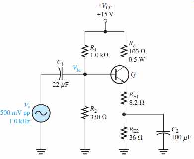
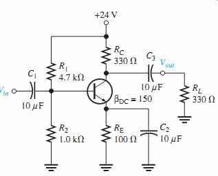
1. FIG. 42 shows a CE power amplifier in which the collector resistor serves also as the load resistor. Assume βDC = βac = 100.
(a) Determine the dc Q-point (ICQ and VCEQ).
(b) Determine the voltage gain and the power gain.
2. For the circuit in FIG. 42, determine the following:
(a) the power dissipated in the transistor with no load (b) the total power from the power supply with no load (c) the signal power in the load with a 500 mV input
3. Refer to the circuit in FIG. 42. What changes would be necessary to convert the circuit to a pnp transistor with a positive supply? What advantage would this have?
4. Assume a CC amplifier has an input resistance of 2.2 k Ω and drives an output load of 50 Ω .
What is the power gain?
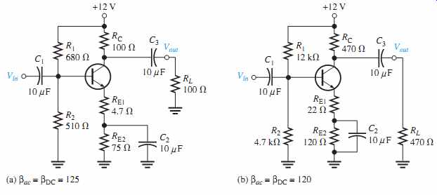
5. Determine the Q-point for each amplifier in FIG. 43.
6. If the load resistor in FIG. 43(a) is changed to 50 Ω , how much does the Q-point change?
7. What is the maximum peak value of collector current that can be realized in each circuit of FIG. 43? What is the maximum peak value of output voltage in each circuit?
8. Find the power gain for each circuit in FIG. 43. Neglect
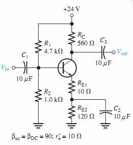
9. Determine the minimum power rating for the transistor in FIG. 44.
10. Find the maximum output signal power to the load and efficiency for the amplifier in FIG. 44 with a load resistor. 500 Ω r’ e.
Section 2 The Class B and Class AB Push-Pull Amplifiers
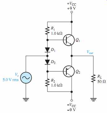
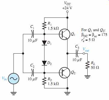
11. Refer to the class AB amplifier in FIG. 45.
(a) Determine the dc parameters VB(Q1), VB(Q2), VE, ICQ, VCEQ(Q1), VCEQ(Q2).
(b) For the 5 V rms input, determine the power delivered to the load resistor.
12. Draw the load line for the npn transistor in FIG. 45. Label the saturation current, Ic(sat), and show the Q-point.
13. Determine the approximate input resistance seen by the signal source for the amplifier of FIG. 45 if 50 Ω βac = 100.
14. If D2 has more voltage drop than D1, what effect does this have on the output?
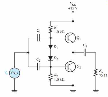
15. Refer to the class AB amplifier in FIG. 46 operating with a single power supply.
(a) Determine the dc parameters VB(Q1), VB(Q2), VE, ICQ, VCEQ(Q1), VCEQ(Q2).
(b) Assuming the input voltage is 10 V pp, determine the power delivered to the load resistor.
16. Refer to the class AB amplifier in FIG. 46.
(a) What is the maximum power that could be delivered to the load resistor? (b) Assume the power supply voltage is raised to 24 V. What is the new maximum power that could be delivered to the load resistor?
17. Refer to the class AB amplifier in FIG. 46. What fault or faults could account for each of the following troubles? (a) a positive half-wave output signal (b) zero volts on both bases and the emitters (c) no output: emitter voltage = -15 V (d) crossover distortion observed on the output waveform
18. If a 1 V rms signal source with an internal resistance of is connected to the amplifier in FIG. 46, what is the actual rms signal applied to the amplifier input? Assume βac = 200.
Section 3 The Class C Amplifier 19. A certain class C amplifier transistor is on for 10 percent of the input cycle. If Vce(sat) = 0.18 V and Ic (sat) = 25 mA, what is the average power dissipation for maximum output?
20. What is the resonant frequency of a tank circuit with L = 10 mH and C = 0.001 mF?
21. What is the maximum peak-to-peak output voltage of a tuned class C amplifier with VCC = 12 V?
22. Determine the efficiency of the class C amplifier described in Problem 21 if VCC =15 V and the equivalent parallel resistance in the collector tank circuit is 50 Ω . Assume that the transistor is on for 10% of the period.
Section 4 Troubleshooting
23. Refer to FIG. 47. What would you expect to observe across RL if C1 opened?
24. Your oscilloscope displays a half-wave output when connected across RL in FIG. 47. What is the probable cause?
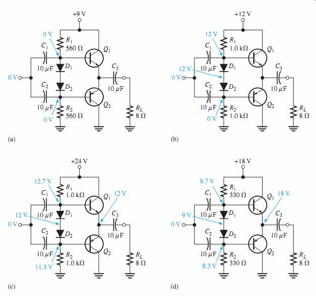
25. Determine the possible fault or faults, if any, for each circuit in FIG. 48 based on the indicated dc voltage measurements.
APPLICATION ACTIVITY PROBLEMS
26. Assume that the public address system represented by the block diagram in FIG. 34 has quit working. You find there is no signal output from the power amplifier or the preamplifier, but you have verified that the microphone is working. Which two blocks are the most likely to be the problem? How would you narrow the choice down to one block?
27. Describe the output that would be observed in the push-pull amplifier of FIG. 35 with a 2 V rms sinusoidal input voltage if the base-emitter junction of Q2 opened.
28. Describe the output that would be observed in FIG. 35 if the collector-emitter junction of Q5 opened for the same input as in Problem 27.
29. After visually inspecting the power amplifier circuit board in FIG. 49, describe any problems.
DATASHEET PROBLEMS
30. Referring to the datasheet in FIG. 50, determine the following:
(a) minimum for the BD135 and the conditions
(b) maximum collector-to-emitter voltage for the BD135
(c) maximum power dissipation for the BD135 at a case temperature of 25°C
(d) maximum continuous collector current for the BD135
31. Determine the maximum power dissipation for a BD135 at a case temperature of 50°C
32. Determine the maximum power dissipation for a BD135 at an ambient temperature of 50°C.
33. Describe what happens to the dc current gain as the collector current increases.
34. Determine the approximate hFE for the BD135 at IC = 20 mA.
ADVANCED PROBLEMS
35. Explain why the specified maximum power dissipation of a power transistor at an ambient temperature of 25°C is much less than maximum power dissipation at a case temperature of 25°C .
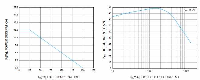
FIG. 50 Copyright Fairchild Semiconductor Corporation. Used by permission.
36. Draw the dc and the ac load lines for the amplifier in FIG. 51.
37. Design a swamped class A power amplifier that will operate from a dc supply of +15 V with an approximate voltage gain of 50. The quiescent collector current should be approximately 500 mA, and the total dc current from the supply should not exceed 750 mA. The output power must be at least 1 W.
38. The public address system in FIG. 34 is a portable unit that is independent of 115 V ac.
Determine the ampere-hour rating for the +15 V and the -15 V battery supply necessary for the system to operate for 4 hours on a continuous basis.


