AMAZON multi-meters discounts AMAZON oscilloscope discounts
OUTLINE:
1. The JFET
2. JFET Characteristics and Parameters
3. JFET Biasing
4. The Ohmic Region
5. The MOSFET
6. MOSFET Characteristics and Parameters
7. MOSFET Biasing
8. The IGBT
9. Troubleshooting
Application Activity
GOALS:
-- Discuss the JFET and how it differs from the BJT
-- Discuss, define, and apply JFET characteristics and parameters
-- Discuss and analyze JFET biasing
-- Discuss the ohmic region on a JFET characteristic curve
-- Explain the operation of MOSFETs
-- Discuss and apply MOSFET parameters
-- Describe and analyze MOSFET bias circuits
-- Discuss the IGBT
-- Troubleshoot FET circuits
TERMINOLOGY:
-- JFET
-- Drain
-- Source
-- Gate
-- Pinch-off voltage
-- Transconductance
-- Ohmic region
-- MOSFET
-- Depletion
-- Enhancement
-- IGBT
INTRODUCTION
BJTs (bipolar junction transistors) were covered in previous sections. Now we will discuss the second major type of transistor, the FET (field-effect transistor). FETs are unipolar devices because, unlike BJTs that use both electron and hole current, they operate only with one type of charge carrier.
The two main types of FETs are the junction field-effect transistor (JFET) and the metal oxide semiconductor field-effect transistor (MOSFET). The term field-effect relates to the depletion region formed in the channel of a FET as a result of a voltage applied on one of its terminals (gate).
Recall that a BJT is a current-controlled device; that is, the base current controls the amount of collector current. A FET is different. It is a voltage-controlled device, where the voltage between two of the terminals (gate and source) controls the current through the device. A major advantage of FETs is their very high input resistance. Because of their nonlinear characteristics, they are generally not as widely used in amplifiers as BJTs except where very high input impedances are required. However, FETs are the preferred device in low-voltage switching applications because they are generally faster than BJTs when turned on and off. The IGBT is generally used in high-voltage switching applications.
1. THE JFET
The JFET ( junction field-effect transistor) is a type of FET that operates with a reverse-biased pn junction to control current in a channel. Depending on their structure, JFETs fall into either of two categories, n channel or p channel.
After reading this section, you should be able to:
-- Discuss the JFET and how it differs from the BJT
-- Describe the basic structure of n-channel and p-channel JFETs
-- Name the terminals ? Explain a channel
-- Explain the basic operation of a JFET
-- Identify JFET schematic symbols
Basic Structure
FIG. 1(a) shows the basic structure of an n-channel JFET (junction field-effect transistor). Wire leads are connected to each end of the n-channel; the drain is at the upper end, and the source is at the lower end. Two p-type regions are diffused in the n-type material to form a channel, and both p-type regions are connected to the gate lead. For simplicity, the gate lead is shown connected to only one of the p regions. A p-channel JFET is shown in FIG. 1(b).
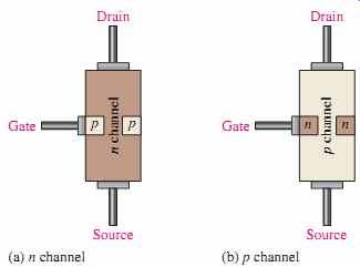
FIG. 1 A representation of the basic structure of the two types of JFET.
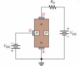
FIG. 2 A biased n-channel JFET.
Basic Operation
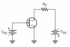
To illustrate the operation of a JFET, FIG. 2 shows dc bias voltages applied to an n-channel device. VDD provides a drain-to-source voltage and supplies current from drain to source. VGG sets the reverse-bias voltage between the gate and the source, as shown.
The JFET is always operated with the gate-source pn junction reverse-biased. Reverse biasing of the gate-source junction with a negative gate voltage produces a depletion region along the pn junction, which extends into the n channel and thus increases its resistance by restricting the channel width.
The channel width and thus the channel resistance can be controlled by varying the gate voltage, thereby controlling the amount of drain current, ID. FIG. 3 illustrates this concept. The white areas represent the depletion region created by the reverse bias. It is wider toward the drain end of the channel because the reverse-bias voltage between the gate and the drain is greater than that between the gate and the source. We will discuss JFET characteristic curves and some parameters in Section 2.
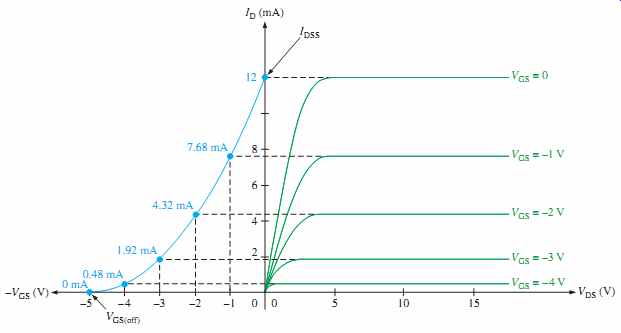
FIG. 3 Effects of VGS on channel width, resistance, and drain current
(VGG= VGS).
(a) JFET biased for conduction (b) Greater VGG narrows the channel (between the white areas) which increases the resistance of the channel and decreases ID.
(c) Less VGG widens the channel (between the white areas) which decreases the resistance of the channel and increases ID.
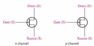
FIG. 4 JFET schematic symbols.
JFET Symbols
The schematic symbols for both n-channel and p-channel JFETs are shown in FIG. 4.
Notice that the arrow on the gate points "in" for n channel and "out" for p channel.
SECTION 1 CHECKUP
1. Name the three terminals of a JFET.
2. Does an n-channel JFET require a positive or negative value for VGS?
3. How is the drain current controlled in a JFET?
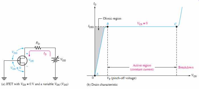
FIG. 5 The drain characteristic curve of a JFET for VGS 0 showing pinch-off
voltage.
2. JFET CHARACTERISTICS AND PARAMETERS
The JFET operates as a voltage-controlled, constant-current device. Cutoff and pinch off as well as JFET transfer characteristics are covered in this section.
After completing this section, you should be able to
-- Discuss, define, and apply JFET characteristics and parameters
-- Discuss the drain characteristic curve
-- Identify the ohmic, active, and breakdown regions of the curve
-- Define pinch-off voltage
-- Discuss breakdown
-- Explain how gate-to-source voltage controls the drain current
-- Discuss the cutoff voltage
-- Compare pinch-off and cutoff
-- Explain the JFET universal transfer characteristic
-- Calculate the drain current using the transfer characteristic equation
-- Interpret a JFET datasheet
-- Discuss JFET forward transconductance
-- Define transconductance
-- Calculate forward transconductance
-- Discuss JFET input resistance and capacitance
-- Determine the ac drain-to-source resistance
Drain Characteristic Curve
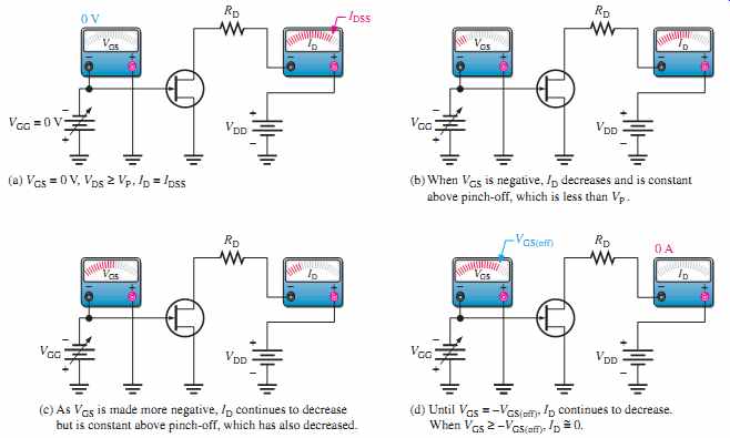
Consider the case when the gate-to-source voltage is zero (VGS = 0 V). This is produced by shorting the gate to the source, as in FIG. 5(a) where both are grounded. As VDD (and thus VDS) is increased from 0 V, ID will increase proportionally, as shown in the graph of FIG. 5(b) between points A and B. In this area, the channel resistance is essentially constant because the depletion region is not large enough to have significant effect. This is called the ohmic region because VDS and ID are related by Ohm's law. (Ohmic region is discussed further in Section 4.) At point B in FIG. 5(b), the curve levels off and enters the active region where ID becomes essentially constant. As VDS increases from point B to point C, the reverse-bias voltage from gate to drain (VGD) produces a depletion region large enough to offset the in crease in VDS, thus keeping ID relatively constant.
Pinch-Off Voltage
For VGS 0 V, the value of VDS at which ID becomes essentially constant (point B on the curve in FIG. 5(b)) is the pinch-off voltage, VP. For a given JFET, VP has a fixed value. As you can see, a continued increase in VDS above the pinch off voltage produces an almost constant drain current. This value of drain current is IDSS (Drain to Source current with gate Shorted) and is always specified on JFET datasheets.
IDSS is the maximum drain current that a specific JFET can produce regardless of the external circuit, and it is always specified for the condition, VGS = 0 V.
Breakdown
As shown in the graph in FIG. 5(b), breakdown occurs at point C when ID begins to increase very rapidly with any further increase in VDS. Breakdown can result in irreversible damage to the device, so JFETs are always operated below breakdown and within the active region (constant current) (between points B and C on the graph). The JFET action that produces the drain characteristic curve to the point of breakdown for VGS 0 V is illustrated in FIG. 6.
VGS Controls ID
Let's connect a bias voltage, VGG, from gate to source as shown in FIG. 7(a). As VGS is set to increasingly more negative values by adjusting VGG, a family of drain characteristic curves is produced, as shown in FIG. 7(b). Notice that ID decreases as the magnitude of VGS is increased to larger negative values because of the narrowing of the channel.
Also notice that, for each increase in VGS, the JFET reaches pinch-off (where constant current begins) at values of VDS less than VP. The term pinch-off is not the same as pinch off voltage, Vp. Therefore, the amount of drain current is controlled by VGS, as illustrated in FIG. 8.

FIG. 5 The drain characteristic curve of a JFET for VGS 0 showing pinch-off
voltage. _ (b) Drain characteristic (a) JFET with VGS = 0 V and a variable
VDS (VDD)
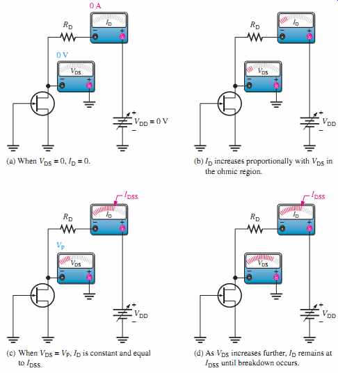
FIG. 6 JFET action that produces the characteristic curve for VGS =0
V. _
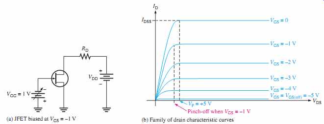
FIG. 7 Pinch-off occurs at a lower VDS as VGS is increased to more negative
values.
Cutoff Voltage
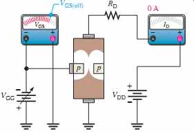
The value of VGS that makes ID approximately zero is the cutoff voltage, VGS(off), as shown in FIG. 8(d). The JFET must be operated between VGS =0 V and VGS(off). For this range of gate-to-source voltages, ID will vary from a maximum of IDSS to a minimum of almost zero.
As you have seen, for an n-channel JFET, the more negative VGS is, the smaller ID be comes in the active region. When VGS has a sufficiently large negative value, ID is reduced to zero. This cutoff effect is caused by the widening of the depletion region to a point where it completely closes the channel, as shown in FIG. 9.
The basic operation of a p-channel JFET is the same as for an n-channel device except that a p-channel JFET requires a negative VDD and a positive VGS, as illustrated in FIG. 10.
Comparison of Pinch-Off Voltage and Cutoff Voltage
As you have seen, there is a difference between pinch-off and cutoff voltages. There is also a connection. The pinch-off voltage VP is the value of VDS at which the drain current becomes constant and equal to IDSS and is always measured at VGS = 0 V. However, pinch-off occurs for VDS values less than VP when VGS is nonzero. So, although VP is a constant, the minimum value of VDS at which ID becomes constant varies with VGS.
VGS(off) and VP are always equal in magnitude but opposite in sign. A datasheet usually will give either VGS(off) or VP, but not both. However, when you know one, you have the other. For example, if then VP 5 V, as shown in FIG. 7(b). + = VGS(off) =-5V,
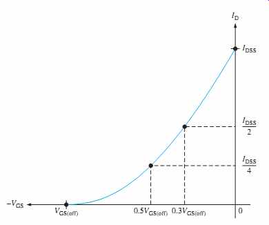
FIG. 12 JFET universal transfer characteristic curve (n-channel).
JFET Universal Transfer Characteristic
You have learned that a range of VGS values from zero to VGS(off) controls the amount of drain current. For an n-channel JFET, VGS(off) is negative, and for a p-channel JFET, VGS(off) is positive. Because VGS does control ID, the relationship between these two quantities is very important. FIG. 12 is a general transfer characteristic curve that illustrates graphically the relationship between VGS and ID. This curve is also known as a transconductance curve.
Notice that the bottom end of the curve is at a point on the VGS axis equal to VGS(off ), and the top end of the curve is at a point on the ID axis equal to IDSS. This curve shows that:
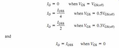
The transfer characteristic curve can also be developed from the drain characteristic curves by plotting values of ID for the values of VGS taken from the family of drain curves at pinch-off, as illustrated in FIG. 13 for a specific set of curves. Each point on the transfer characteristic curve corresponds to specific values of VGS and ID on the drain curves. For example, when Also, for this specific JFET, and IDSS = 12 mA. VGS(off) =-5V VGS =-2V, ID = 4.32 mA.

FIG. 13 Example of the development of an n-channel JFET transfer characteristic
curve (blue) from the JFET drain characteristic curves (green).
A JFET transfer characteristic curve is expressed approximately as
With Equation 1, ID can be determined for any VGS if VGS(off) and IDSS are known. These quantities are usually available from the datasheet for a given JFET. Notice the squared term in the equation. Because of its form, a parabolic relationship is known as a square law, and therefore, JFETs and MOSFETs are often referred to as square-law devices.
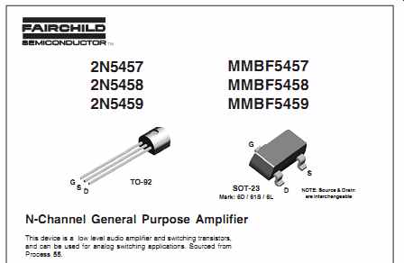
The datasheet for a typical JFET series is shown in FIG. 14.
JFET partial datasheet. Copyright Fairchild Semiconductor Corporation.
JFET Forward Transconductance
The forward transconductance (transfer conductance), gm, is the change in drain current (delta_ID) for a given change in gate-to-source voltage (delta_VGS) with the drain-to-source voltage constant. It is expressed as a ratio and has the unit of siemens (S).
gm = delta_ID / delta_VGS
Other common designations for this parameter are gfs and yfs (forward transfer admittance). As you will see in Section 9, gm is an important factor in determining the voltage gain of a FET amplifier.
Because the transfer characteristic curve for a JFET is nonlinear, gm varies in value depending on the location on the curve as set by VGS. The value for gm is greater near the top of the curve (near VGS = 0) than it is near the bottom (near VGS(off)), as illustrated in FIG. 15.
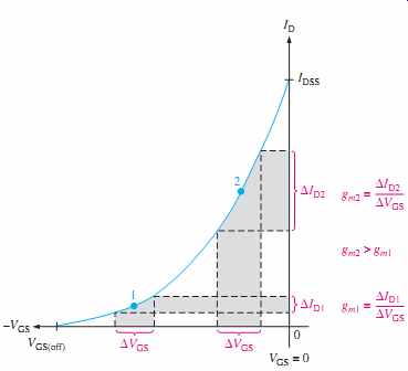
FIG. 15 gm varies depending on the bias point (VGS).
A datasheet normally gives the value of gm measured at VGS = 0V(gm0). For example, the datasheet for the 2N5457 JFET specifies a minimum gm0 (gfs) of (the mho is the same unit as the siemens (S)) with VDS = 15 V.
Given gm0, you can calculate an approximate value for gm at any point on the transfer characteristic curve using the following formula:
1000 mmhos
When a value of gm0 is not available, you can calculate it using values of IDSS and VGS(off ). The vertical lines indicate an absolute value (no sign).
Input Resistance and Capacitance
As you know, a JFET operates with its gate-source junction reverse-biased, which makes the input resistance at the gate very high. This high input resistance is one advantage of the JFET over the BJT. (Recall that a bipolar junction transistor operates with a forward-biased base-emitter junction.) JFET datasheets often specify the input resistance by giving a value for the gate reverse current, IGSS, at a certain gate-to-source voltage. The input resistance can then be determined using the following equation, where the vertical lines indicate an absolute value (no sign):
RIN = VGS/IGSS
For example, the 2N5457 datasheet in FIG. 14 lists a maximum IGSS of -1.0 nA for VGS =-15 V at 25°C. IGSS increases with temperature, so the input resistance decreases.
The input capacitance, Ciss, is a result of the JFET operating with a reverse-biased pn junction. Recall that a reverse-biased pn junction acts as a capacitor whose capacitance depends on the amount of reverse voltage. For example, the 2N5457 has a maximum Ciss of 7 pF for VGS = 0.
AC Drain-to-Source Resistance
You learned from the drain characteristic curve that, above pinch-off, the drain current is relatively constant over a range of drain-to-source voltages. Therefore, a large change in VDS produces only a very small change in ID. The ratio of these changes is the ac drain-to source resistance of the device,
r' ds
r’ ds = delta_VDS/delta_ID
Datasheets often specify this parameter in terms of the output conductance, gos, or output admittance, yos, for VGS = 0 V.
SECTION 2 CHECKUP
1. The drain-to-source voltage at the pinch-off point of a particular JFET is 7 V. If the gate-to-source voltage is zero, what is VP?
2. The VGS of a certain n-channel JFET is increased negatively. Does the drain current increase or decrease?
3. What value must VGS have to produce cutoff in a p-channel JFET with a Vp =3 V?
3. JFET BIASING
Using some of the JFET parameters discussed previously, you will now see how to dc-bias JFETs. Just as with the BJT, the purpose of biasing is to select the proper dc gate-to-source voltage to establish a desired value of drain current and, thus, a proper Q-point. Three types of bias are self-bias, voltage-divider bias, and current-source bias.
After completing this section, you should be able to:
-- Discuss and analyze JFET biasing
-- Describe self-bias
-- Calculate JFET currents and voltages
-- Describe how to set the Q-point of a self-biased JFET
-- Determine midpoint bias
-- Graphically analyze a self-biased JFET
-- Discuss voltage-divider bias
-- Calculate JFET currents and voltages
-- Graphically analyze a voltage-divider biased JFET
-- Discuss Q-point stability
-- Describe current-source bias
Self-Bias
Self-bias is the most common type of JFET bias. Recall that a JFET must be operated such that the gate-source junction is always reverse-biased. This condition requires a negative VGS for an n-channel JFET and a positive VGS for a p-channel JFET. This can be achieved using the self-bias arrangements shown in FIG. 16. The gate resistor, RG, does not affect the bias because it has essentially no voltage drop across it; and therefore the gate re mains at 0 V. RG is necessary only to force the gate to be at 0 V and to isolate an ac signal from ground in amplifier applications, as you will see later.
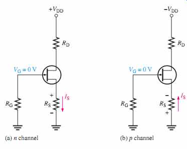
FIG. 16 Self-biased JFETs (IS = ID in all FETs).
For the n-channel JFET in FIG. 16(a), IS produces a voltage drop across RS and makes the source positive with respect to ground. Since IS =ID and VG =0, then VS =IDRS.
The gate-to-source voltage is:
VGS =+IDRS VGS =-IDRS
Thus,
For the p-channel JFET shown in FIG. 16(b), the current through RS produces a negative voltage at the source, making the gate positive with respect to the source. Therefore, since IS = ID,
In the following example, the n-channel JFET in FIG. 16(a) is used for illustration.
Keep in mind that analysis of the p-channel JFET is the same except for opposite-polarity voltages. The drain voltage with respect to ground is determined as follows:
VD = VDD - IDRD
Since VS = IDRS, the drain-to-source voltage is:
VDS = VD - VS = VDD - ID(RD + RS)
VGS = VG - VS = 0 - IDRS =-IDRS
Setting the Q-Point of a Self-Biased JFET
The basic approach to establishing a JFET bias point is to determine ID for a desired value of VGS or vice versa. Then calculate the required value of RS using the following relation ship. The vertical lines indicate an absolute value.
RS = |VGS/ID|
For a desired value of VGS, ID can be determined in either of two ways: from the transfer characteristic curve for the particular JFET or, more practically, from Equation 1 using IDSS and VGS(off) from the JFET datasheet. The next two examples illustrate these procedures.
Midpoint Bias
It is usually desirable to bias a JFET near the midpoint of its transfer characteristic curve where ID= IDSS_2. Under signal conditions, midpoint bias allows the maximum amount of drain current swing between IDSS and 0. For Equation 1, it can be shown that ID is approximately one-half of IDSS when VGS = VGS(off)_3.4. The derivation is given in "Derivations of Selected Equations”.

So, by selecting VGS = VGS(off )/3.4, you should get a midpoint bias in terms of ID.
To set the drain voltage at midpoint (VD = VDD/2), select a value of RD to produce the desired voltage drop. Choose RG arbitrarily large to prevent loading on the driving stage in a cascaded amplifier arrangement. Example 9 illustrates these concepts.
Graphical Analysis of a Self-Biased JFET
You can use the transfer characteristic curve of a JFET and certain parameters to deter mine the Q-point (ID and VGS) of a self-biased circuit. A circuit is shown in FIG. 20(a), and a transfer characteristic curve is shown in FIG. 20(b). If a curve is not available from a datasheet, you can plot it from Equation 1 using datasheet values for IDSS and VGS(off ).
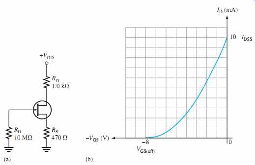
FIG. 20 A self-biased JFET and its transfer characteristic curve.
To determine the Q-point of the circuit in FIG. 20(a), a self-bias dc load line is established on the graph in part (b) as follows. First, calculate VGS when ID is zero.
VGS =-IDRS = (0)(470 ohm) = 0V
This establishes a point at the origin on the graph (ID 0, VGS 0). Next, calculate VGS when ID IDSS. From the curve in FIG. 20(b), IDSS=10 mA.
VGS =-IDRS =-(10 mA)(470 OHM) =-4.7 V
This establishes a second point on the graph (ID = 10 mA, VGS =-4.7 V). Now, with two points, the load line can be drawn on the transfer characteristic curve as shown in FIG. 21. The point where the load line intersects the transfer characteristic curve is the Q-point of the circuit as shown, where ID = 5.07 mA and VGS =-2.3 V.
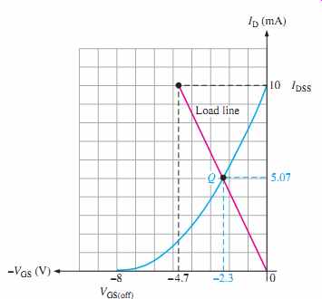
FIG. 21 The intersection of the self-bias dc load line and the transfer
characteristic curve is the Q-point.
For increased Q-point stability, the value of RS in the self-bias circuit is increased and connected to a negative supply voltage. This is sometimes called dual-supply bias.
Voltage-Divider Bias
An n-channel JFET with voltage-divider bias is shown in FIG. 23. The voltage at the source of the JFET must be more positive than the voltage at the gate in order to keep the gate-source junction reverse-biased.
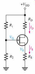
FIG. 23 An n-channel JFET with voltage divider bias (IS ID). _
The source voltage is:
VS = IDRS
The gate voltage is set by resistors R1 and R2 as expressed by the following equation using the voltage-divider formula:
The gate-to-source voltage is and the source voltage is
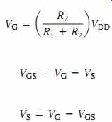
The drain current can be expressed as
Substituting for VS,

Graphical Analysis of a JFET with Voltage-Divider Bias
An approach similar to the one used for self-bias can be used with voltage-divider bias to graphically determine the Q-point of a circuit on the transfer characteristic curve.
In a JFET with voltage-divider bias when ID=0, VGS is not zero, as in the self-biased case, because the voltage divider produces a voltage at the gate independent of the drain current. The voltage-divider dc load line is determined as follows.
For ID 0,
VS = IDRS = (0)RS = 0V
VGS = VG - VS = VG - 0V = VG
Therefore, one point on the line is at ID=0 and VGS=VG.
For VGS 0, =
A second point on the line is at ID VG/RS and VGS 0. The generalized dc load line is shown in FIG. 25. The point at which the load line intersects the transfer characteristic curve is the Q-point.
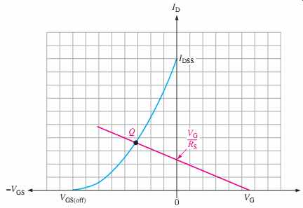
FIG. 25 Generalized dc load line (red) for a JFET with voltage-divider
bias.
Q-Point Stability
Unfortunately, the transfer characteristic of a JFET can differ considerably from one device to another of the same type. If, for example, a 2N5459 JFET is replaced in a given bias circuit with another 2N5459, the transfer characteristic curve can vary greatly, as illustrated in FIG. 27(a). In this case, the maximum IDSS is 16 mA and the minimum IDSS is 4 mA. Likewise, the maximum VGS(off ) is -8Vand the minimum VGS(off ) is -2V. This means that if you have a selection of 2N5459s and you randomly pick one out, it can have values anywhere within these ranges.
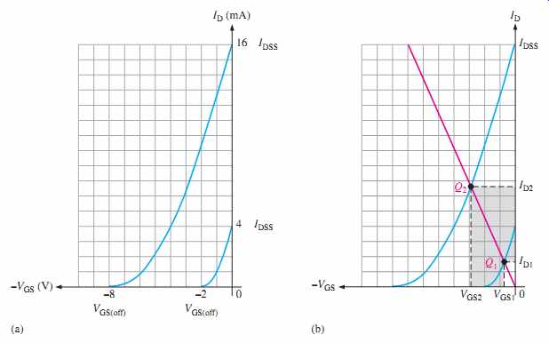
FIG. 27 Variation in the transfer characteristic of 2N5459 JFETs and
the effect on the Q-point.
If a self-bias dc load line is drawn as illustrated in FIG. 27(b), the same circuit using a 2N5459 can have a Q-point anywhere along the line from Q1, the minimum bias point, to Q2, the maximum bias point. Accordingly, the drain current can be any value between ID1 and ID2, as shown by the shaded area. This means that the dc voltage at the drain can have a range of values depending on ID. Also, the gate-to-source voltage can be any value between VGS1 and VGS2, as indicated.
FIG. 28 illustrates Q-point stability for a self-biased JFET and for a JFET with voltage divider bias. With voltage-divider bias, the dependency of ID on the range of Q-points is reduced because the slope of the load line is less than for self-bias for a given JFET.
Although VGS varies quite a bit for both self-bias and voltage-divider bias, ID is much more stable with voltage-divider bias.
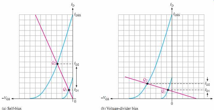
FIG. 28 The change in ID between the minimum and the maximum Q-points
is much less for a JFET with voltage-divider bias than for a self-biased
JFET.
Current-Source Bias
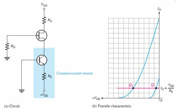
Current-source bias is a method for increasing the Q-point stability of a self-biased JFET by making the drain current essentially independent of VGS. This is accomplished by using a constant-current source in series with the JFET source, as shown in FIG. 29(a). In this circuit, a BJT acts as the constant-current source because its emitter current is essentially constant if A FET can also be used as a constant current source.
VEE W VBE.
Since IE= ID,

As you can see in FIG. 29(b), ID remains constant for any transfer characteristic curve, as indicated by the horizontal load line.
SECTION 3 CHECKUP
1. Should a p-channel JFET have a positive or a negative VGS?
2. In a certain self-biased n-channel JFET circuit, and Deter mine VGS.
3. An n-channel JFET with voltage-divider bias has a gate voltage of 3 V and a source volt age of 5 V. Calculate VGS.
RS = 1.0 k-OHM. ID = 8mA
4. THE OHMIC REGION
The ohmic region is the portion of the FET characteristic curves in which Ohm's law can be applied. When properly biased in the ohmic region, a JFET exhibits the properties of a variable resistance, where the value of resistance is controlled by VGS.
After completing this section, you should be able to:
-- Discuss the ohmic region on a JFET characteristic curve
-- Calculate slope and drain-to-source resistance
-- Explain how a JFET can be used as a variable resistance
-- Discuss JFET operation with the Q-point at the origin
-- Calculate transconductance
The ohmic region extends from the origin of the characteristic curves to the break point (where the active region begins) of the VGS=0 curve in a roughly parabolic shape, as shown on a typical set of curves in FIG. 30. The characteristic curves in this region have a relatively constant slope for small values of ID. The slope of the characteristic curve in the ohmic region is the dc drain-to-source conductance GDS of the JFET.

Recall from your basic circuits course that resistance is the reciprocal of the conductance.
Thus, the dc drain-to-source resistance is given by

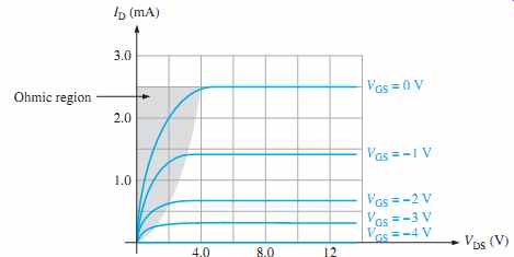
FIG. 30 The ohmic region is the shaded area.
The JFET as a Variable Resistance A JFET can be biased in either the active region or the ohmic region. JFETs are often biased in the ohmic region for use as a voltage controlled variable resistor. The control voltage is VGS, and it determines the resistance by varying the Q-point. To bias a JFET in the ohmic region, the dc load line must intersect the characteristic curve in the ohmic region, as illustrated in FIG. 31. To do this in a way that allows VGS to control RDS, the dc saturation current is set for a value much less than IDSS so that the load line intersects most of the characteristic curves in the ohmic region, as

FIG. 31 shows the operating region expanded with three Q-points shown (Q0, Q1, and Q2), depending on VGS.
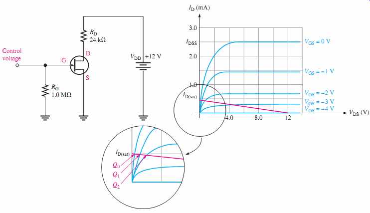
FIG. 31 The load line intersects the curves inside the ohmic region.
As you move along the load line in the ohmic region of FIG. 31, the value of RDS varies as the Q-point falls successively on curves with different slopes. The Q-point is moved along the load line by varying VGS =0 to VGS = -2v in this case. As this happens, the slope of each successive curve is less than the previous one. A decrease in slope corresponds to less ID and more VDS, which implies an increase in RDS. This change in resistance can be exploited in a number of applications where voltage control of a resistance is useful.
Q-point at the Origin
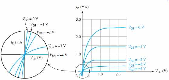
In certain amplifiers, you may want to change the resistance seen by the ac signal without affecting the dc bias in order to control the gain. Sometimes you will see a JFET used as a variable resistance in a circuit where both ID and VDS are set at 0, which means that the Q-point is at the origin. A Q-point at the origin is achieved by using a capacitor in the drain circuit of the JFET. This makes the dc quantities VDS=0 V and ID=0 mA, so the only variables are VGS and Id, the ac drain current. At the origin you have the ac drain current controlled by VGS. As you learned earlier, transconductance is defined as a change in drain current for a given change in gate-to-source voltage. So, the key factor when you bias at the origin is the transconductance. FIG. 33 shows the characteristic curves expanded at the origin. Notice that the ohmic region extends into the third quadrant.
At the origin, where VDS=0 V and ID=0 mA, the formula for transconductance, introduced earlier in this section, is:

where gm is transconductance and gm0 is transconductance for VGS=0V. gm0 can be calculated from the following equation, which was also given earlier:

SECTION 4 CHECKUP
1. For a certain Q-point in the ohmic region, ID = 0.3 mA and VDS = 0.6 V. What is the resistance of the JFET when it is biased at this Q-point?
2. How does the drain-to-source resistance change as VGS becomes more negative?
3. For a JFET biased at the origin, gm=0.850 mS. Determine the corresponding ac resistance.
5. THE MOSFET
The MOSFET (metal oxide semiconductor field-effect transistor) is another category of field-effect transistor. The MOSFET, different from the JFET, has no pn junction structure; instead, the gate of the MOSFET is insulated from the channel by a silicon dioxide (SiO2) layer. The two basic types of MOSFETs are enhancement (E) and depletion (D). Of the two types, the enhancement MOSFET is more widely used. Because polycrystalline silicon is now used for the gate material instead of metal, these devices are sometimes called IGFETs (insulated-gate FETs).
After completing this section, you should be able to:
-- Explain the operation of MOSFETs
-- Discuss the enhancement MOSFET (E-MOSFET)
-- Describe the structure
-- Identify the symbols for E-MOSFET n-channel and p-channel devices
-- Discuss the depletion MOSFET (D-MOSFET)
-- Describe the structure
-- Discuss the depletion and enhancement modes
-- Identify the symbols for D-MOSFET n-channel and p-channel devices
-- Discuss power MOSFETs
-- Describe LDMOSFET structure
-- Describe VMOSFET structure
-- Describe TMOSFET structure
-- Describe the dual-gate MOSFET
-- Identify the symbols for dual-gate D-MOSFETs and E-MOSFETs
Enhancement MOSFET (E-MOSFET)
The E-MOSFET operates only in the enhancement mode and has no depletion mode. It differs in construction from the D-MOSFET, which is discussed next, in that it has no structural channel. Notice in FIG. 34(a) that the substrate extends completely to the SiO2 layer. For an n-channel device, a positive gate voltage above a threshold value induces a channel by creating a thin layer of negative charges in the substrate region adjacent to the SiO2 layer, as shown in FIG. 34(b). The conductivity of the channel is enhanced by increasing the gate-to-source voltage and thus pulling more electrons into the channel area. For any gate voltage below the threshold value, there is no channel.
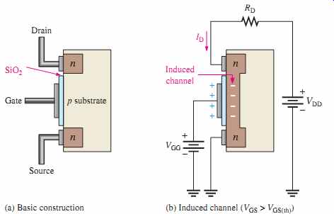
FIG. 34 Representation of the basic E-MOSFET construction and operation
(n-channel).
The schematic symbols for the n-channel and p-channel E-MOSFETs are shown in FIG. 35. The broken lines symbolize the absence of a physical channel. An inward pointing substrate arrow is for n channel, and an outward-pointing arrow is for p channel.
Some E-MOSFET devices have a separate substrate connection.
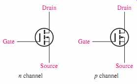
FIG. 35 E-MOSFET schematic symbols.
Depletion MOSFET (D-MOSFET) Another type of MOSFET is the depletion MOSFET (D-MOSFET), and FIG. 36 illustrates its basic structure. The drain and source are diffused into the substrate material and then connected by a narrow channel adjacent to the insulated gate. Both n-channel and p-channel devices are shown in the figure. We will use the n-channel device to describe the basic operation. The p-channel operation is the same, except the voltage polarities are opposite those of the n-channel.
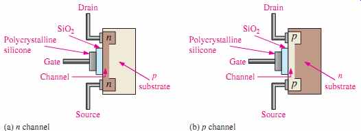
FIG. 36 Representation of the basic structure of D-MOSFETs.
The D-MOSFET can be operated in either of two modes-the depletion mode or the enhancement mode-and is sometimes called a depletion/enhancement MOSFET.
Since the gate is insulated from the channel, either a positive or a negative gate voltage can be applied. The n-channel MOSFET operates in the depletion mode when a negative gate-to-source voltage is applied and in the enhancement mode when a positive gate-to-source voltage is applied. These devices are generally operated in the depletion mode.
Depletion Mode Visualize the gate as one plate of a parallel-plate capacitor and the channel as the other plate. The silicon dioxide insulating layer is the dielectric. With a negative gate voltage, the negative charges on the gate repel conduction electrons from the channel, leaving positive ions in their place. Thereby, the n channel is depleted of some of its electrons, thus decreasing the channel conductivity. The greater the negative voltage on the gate, the greater the depletion of n-channel electrons. At a sufficiently negative gate-to-source voltage, VGS(off ), the channel is totally depleted and the drain current is zero. This depletion mode is illustrated in FIG. 37(a). Like the n-channel JFET, the n-channel D-MOSFET conducts drain current for gate-to-source voltages between VGS(off ) and zero. In addition, the D-MOSFET conducts for values of VGS above zero.
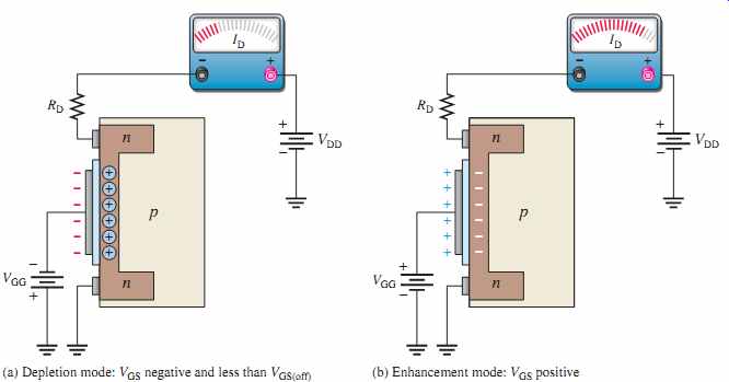
FIG. 37 Operation of n-channel D-MOSFET.
Enhancement Mode
With a positive gate voltage, more conduction electrons are attracted into the channel, thus increasing (enhancing) the channel conductivity, as illustrated in FIG. 37(b).
D-MOSFET Symbols The schematic symbols for both the n-channel and the p-channel depletion MOSFETs are shown in FIG. 38. The substrate, indicated by the arrow, is normally (but not always) connected internally to the source. Sometimes, there is a separate substrate pin.
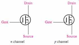
FIG. 38 D-MOSFET schematic symbols.
FYI A new type of field-effect transistor uses a fin-like structure instead of the conventional flat silicon structure. It is much smaller than the conventional silicon transistors.
The fins are made from a semiconductor material called indium-gallium-arsenide instead of silicon. In addition to making computer chips much smaller in size, the finFET can operate many times faster than conventional FETs.
Power MOSFET Structures
The conventional enhancement MOSFETs have a long thin lateral channel as shown in the structural view in FIG. 39. This results in a relatively high drain-to-source resistance and limits the E-MOSFET to low power applications. When the gate is positive, the channel is formed close to the gate between the source and the drain, as shown.
Laterally Diffused MOSFET (LDMOSFET) The LDMOSFET has a lateral channel structure and is a type of enhancement MOSFET designed for power applications.
This device has a shorter channel between drain and source than does the conventional E-MOSFET. The shorter channel results in lower resistance, which allows higher current and voltage.
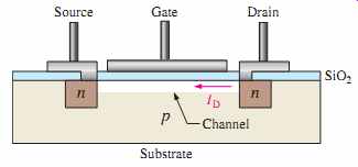
FIG. 39 Cross section of conventional E-MOSFET structure. Channel is
shown as white area.
FIG. 40 shows the basic structure of an LDMOSFET. When the gate is positive, a very short n channel is induced in the p layer between the lightly doped source and the n region. There is current between the drain and source through the n regions and the induced channel as indicated.
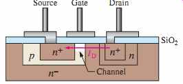
FIG. 40 Cross section of LDMOSFET lateral channel structure.
VMOSFET The V-groove MOSFET is another example of the conventional E-MOSFET designed to achieve higher power capability by creating a shorter and wider channel with less resistance between the drain and source using a vertical channel structure. The shorter, wider channels allow for higher currents and, thus, greater power dissipation. Frequency response is also improved.
The VMOSFET has two source connections, a gate connection on top, and a drain connection on the bottom, as shown in FIG. 41. The channel is induced vertically along both sides of the V-shaped groove between the drain (n+ substrate where n+ means a higher doping level than ) and the source connections. The channel length is set by the thickness of the layers, which is controlled by doping densities and diffusion time rather than by mask dimensions.
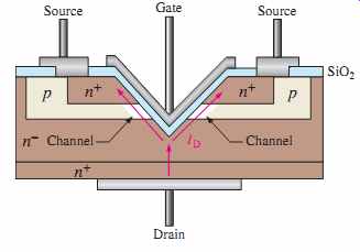
FIG. 41 Cross section of VMOSFET vertical channel structure.
TMOSFET
The vertical channel structure of the TMOSFET is illustrated in FIG. 42.
The gate structure is embedded in a silicon dioxide layer, and the source contact is continuous over the entire surface area. The drain is on the bottom. TMOSFET achieves greater packing density than VMOSFET, while retaining the short vertical channel advantage.
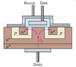
FIG. 42 Cross section of TMOSFET vertical channel structure.
Dual-Gate MOSFETs
The dual-gate MOSFET can be either a depletion or an enhancement type. The only difference is that it has two gates, as shown in FIG. 43. As previously mentioned, one drawback of a FET is its high input capacitance, which restricts its use at higher frequencies. By using a dual-gate device, the input capacitance is reduced, thus making the device useful in high-frequency RF amplifier applications. Another advantage of the dual-gate arrangement is that it allows for an automatic gain control (AGC) input in RF amplifiers.
Another application is demonstrated in the Application Activity where the bias on the second gate is used to adjust the transconductance curve.
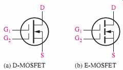
FIG. 43 Dual-gate n-channel MOSFET symbols.
SECTION 5 CHECKUP
1. Name the two basic types of MOSFETs.
2. If the gate-to-source voltage in an n-channel E-MOSFET is made more positive, does the drain current increase or decrease?
3. If the gate-to-source voltage in an n-channel depletion MOSFET is made more negative, does the drain current increase or decrease?
