AMAZON multi-meters discounts AMAZON oscilloscope discounts
<< cont. from part 1
6. MOSFET CHARACTERISTICS AND PARAMETERS
Much of the discussion concerning JFET characteristics and parameters applies equally to MOSFETs. In this section, MOSFET parameters are discussed.
Goals:
-- Discuss and apply MOSFET parameters
-- Describe an E-MOSFET transfer characteristic curve
-- Calculate drain current using an equation for the curve
-- Use an E-MOSFET datasheet
-- Describe a D-MOSFET transfer characteristic curve
-- Calculate drain current using an equation for the curve
-- Discuss the handling precautions for MOSFETS
-- Explain why MOSFETs must be handled properly
-- List the precautions
E-MOSFET Transfer Characteristic
The E-MOSFET uses only channel enhancement. Therefore, an n-channel device requires a positive gate-to-source voltage, and a p-channel device requires a negative gate-to-source voltage. FIG. 44 shows the general transfer characteristic curves for both types of E-MOSFETs. As you can see, there is no drain current when VGS=0. Therefore, the E-MOSFET does not have a significant IDSS parameter, as do the JFET and the D-MOSFET.
Notice also that there is ideally no drain current until VGS reaches a certain nonzero value called the threshold voltage, VGS(th).
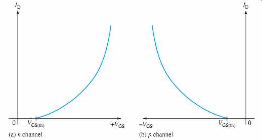
FIG. 44 E-MOSFET general transfer characteristic curves.
The equation for the parabolic transfer characteristic curve of the E-MOSFET differs from that of the JFET and the D-MOSFET because the curve starts at VGS(th) rather than VGS(off ) on the horizontal axis and never intersects the vertical axis. The equation for the E-MOSFET transfer characteristic curve is:
Equation 4
ID = K(VGS -VGS(th)) ^2
The constant K depends on the particular MOSFET and can be determined from the datasheet by taking the specified value of ID, called ID(on), at the given value of VGS and substituting the values into Equation 4 as illustrated in Example 16.
D-MOSFET Transfer Characteristic
As previously discussed, the D-MOSFET can operate with either positive or negative gate voltages. This is indicated on the general transfer characteristic curves in FIG. 45 for both n-channel and p-channel MOSFETs. The point on the curves where VGS=0 corresponds to IDSS. The point where ID=0 corresponds to VGS(off). As with the JFET, VGS(off) =-VP. The square-law expression in Equation 1 for the JFET curve also applies to the D-MOSFET curve, as Example 17 demonstrates.
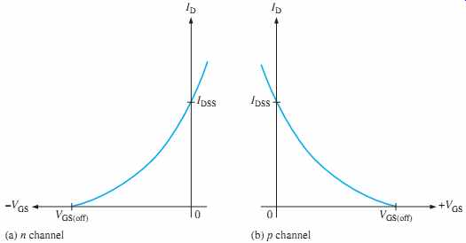
FIG. 45 D-MOSFET general transfer characteristic curves.
Handling Precautions
All MOS devices are subject to damage from electrostatic discharge (ESD). Because the gate of a MOSFET is insulated from the channel, the input resistance is extremely high (ideally infinite). The gate leakage current, IGSS, for a typical MOSFET is in the pA range, whereas the gate reverse current for a typical JFET is in the nA range. The input capacitance results from the insulated gate structure. Excess static charge can be accumulated because the input capacitance combines with the very high input resistance and can result in damage to the device. To avoid damage from ESD, certain precautions should be taken when handling MOSFETs:
1. Carefully remove MOSFET devices from their packaging. They are shipped in conductive foam or special foil conductive bags. Usually they are shipped with a wire ring around the leads, which is removed just prior to installing the MOSFET in a circuit.
2. All instruments and metal benches used in assembly or test should be connected to earth ground (round or third prong of 110 V wall outlets).
3. The assembler's or handler's wrist should be connected to a commercial grounding strap, which has a high-value series resistor for safety. The resistor prevents accidental contact with voltage from becoming lethal.
4. Never remove a MOS device (or any other device, for that matter) from the circuit while the power is on.
5. Do not apply signals to a MOS device while the dc power supply is off.
SECTION 6 CHECKUP
1. What is the major difference in construction of the D-MOSFET and the E-MOSFET?
2. Name two parameters of an E-MOSFET that are not specified for D-MOSFETs?
3. What is ESD?
7. MOSFET BIASING
Three ways to bias a MOSFET are zero-bias, voltage-divider bias, and drain-feedback bias. Biasing is important in FET amplifiers, which you will study in the next section.
After completing this section, you should be able to
-- Describe and analyze MOSFET bias circuits
-- Analyze E-MOSFET bias
-- Discuss and analyze voltage-divider bias ? Discuss and analyze drain-feedback bias
-- Analyze D-MOSFET bias
-- Discuss and analyze zero bias
E-MOSFET Bias
Because E-MOSFETs must have a VGS greater than the threshold value, VGS(th), zero bias cannot be used. FIG. 46 shows two ways to bias an E-MOSFET (D-MOSFETs can also be biased using these methods). An n-channel device is used for purposes of illustration. In either the voltage-divider or drain-feedback bias arrangement, the purpose is to make the gate voltage more positive than the source by an amount exceeding VGS(th).
Equations for the analysis of the voltage-divider bias in FIG. 46(a) are as follows:

where ID = K(VGS - VGS(th))^2 from Equation 4.
In the drain-feedback bias circuit in FIG. 46(b), there is negligible gate current and, therefore, no voltage drop across RG. This makes VGS=VDS.
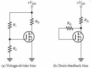
FIG. 46 Common E-MOSFET biasing arrangements.
D-MOSFET Bias
Recall that D-MOSFETs can be operated with either positive or negative values of VGS. A simple bias method is to set VGS=0 so that an ac signal at the gate varies the gate-to source voltage above and below this 0 V bias point. A MOSFET with zero bias is shown in FIG. 49(a). Since VGS=0, ID =IDSS as indicated. The drain-to-source voltage is expressed as follows:
VDS = VDD – IDSS RD
The purpose of RG is to accommodate an ac signal input by isolating it from ground, as shown in FIG. 49(b). Since there is no dc gate current, RG does not affect the zero gate-to-source bias.
SECTION 7 CHECKUP
1. For a D-MOSFET biased at VGS= 0, is the drain current equal to zero, IGSS, or IDSS?
2. For an n-channel E-MOSFET with VGS(th) = 2V, VGS must be in excess of what value in order to conduct?
8. THE IGBT
The IGBT (insulated-gate bipolar transistor) combines features from both the MOSFET and the BJT that make it useful in high-voltage and high-current switching applications. The IGBT has largely replaced the MOSFET and the BJT in many of these applications.
After completing this section, you should be able to
-- Discuss the IGBT
-- Compare the IGBT to the MOSFET and the BJT
-- Identify the IGBT symbol
-- Describe IGBT operation
-- Explain how an IGBT is turned on and off
-- Discuss and analyze drain feedback bias
-- Describe the IGBT equivalent circuit
The IGBT is a device that has the output conduction characteristics of a BJT but is voltage controlled like a MOSFET; it is an excellent choice for many high-voltage switching applications. The IGBT has three terminals: gate, collector, and emitter. One common circuit symbol is shown in FIG. 51. As you can see, it is similar to the BJT symbol except there is an extra bar representing the gate structure of a MOSFET rather than a base.
The IGBT has MOSFET input characteristics and BJT output characteristics. BJTs are capable of higher currents than FETs, but MOSFETs have no gate current because of the insulated gate structure. IGBTs exhibit a lower saturation voltage than MOSFETs and have about the same saturation voltage as BJTs. IGBTs are superior to MOSFETs in some applications because they can handle high collector-to-emitter voltages exceeding 200 V and exhibit less saturation voltage when they are in the on state. IGBTs are superior to BJTs in some applications because they can switch faster. In terms of switching speed, MOSFETs switch fastest, then IGBTs, followed by BJTs, which are slowest. A general comparison of IGBTs, MOSFETs, and BJTs is given in Table 1.
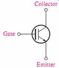
FIG. 51 A symbol for the IGBT (insulated gate bipolar transistor).
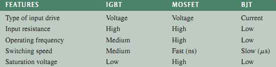
TABLE 1 Comparison of several device features for switching applications.
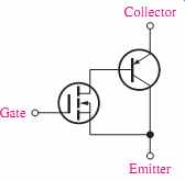
FIG. 52 Simplified equivalent circuit for an IGBT.
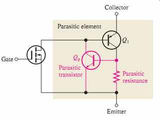
FIG. 53 Parasitic components of an IGBT that can cause latch-up.
Operation
The IGBT is controlled by the gate voltage just like a MOSFET. Essentially, an IGBT can be thought of as a voltage-controlled BJT, but with faster switching speeds. Because it is controlled by voltage on the insulated gate, the IGBT has essentially no input current and does not load the driving source. A simplified equivalent circuit for an IGBT is shown in FIG. 52. The input element is a MOSFET, and the output element is a bipolar transistor. When the gate voltage with respect to the emitter is less than a threshold voltage, Vthresh, the device is turned off. The device is turned on by increasing the gate voltage to a value exceeding the threshold voltage.
The npnp structure of the IGBT forms a parasitic transistor and an inherent parasitic resistance within the device, as shown in red in FIG. 53. These parasitic components have no effect during normal operation. However, if the maximum collector current is exceeded under certain conditions, the parasitic transistor, Qp can turn on. If Qp turns on, it effectively combines with Q1 to form a parasitic element, as shown in FIG. 53, in which a latchup condition can occur. In latch-up, the device will stay on and cannot be con trolled by the gate voltage. Latch-up can be avoided by always operating within the specified limits of the device.
SECTION 8 CHECKUP
1. What does IGBT stand for?
2. What is a major application area for IGBTs?
3. Name an advantage of an IGBT over a power MOSFET.
4. Name an advantage of an IGBT over a power BJT.
5. What is latch-up?
9. TROUBLESHOOTING
In this section, some common faults that may be encountered in FET circuits and the probable causes for each fault are discussed.
After completing this section, you should be able to:
-- Troubleshoot FET circuits
-- Determine faults in self-biased JFET circuits
-- Determine faults in MOSFET circuits
-- Troubleshoot a D-MOSFET with zero bias
-- Troubleshoot an E-MOSFET with voltage-divider bias
Faults in Self-Biased JFET Circuits
FIG. 54 Two symptoms in a self-biased JFET circuit.
Symptom 1: VD = VDD
For this condition, the drain current must be zero because there is no voltage drop across RD, as illustrated in FIG. 54(a). As in any circuit, it is good troubleshooting practice to first check for obvious problems such as open or poor connections, as well as charred resistors. Next, disconnect power and measure suspected resistors for opens. If these are okay, the JFET is probably bad. Any of the following faults can pro duce this symptom:
1. No ground connection at RS
2. RS open
3. Open drain lead connection
4. Open source lead connection
5. FET internally open between drain and source
Symptom 2: VD Significantly Less Than Normal
For this condition, unless the supply voltage is lower than it should be, the drain current must be larger than normal because the drop across RD is too much. FIG. 54(b) indicates this situation. This symptom can be caused by any of the following:
1. Open RG
2. Open gate lead
3. FET internally open at gate
Any of these three faults will cause the depletion region in the JFET to disappear and the channel to widen so that the drain current is limited only by RD, RS, and the small channel resistance.
Faults in D-MOSFET and E-MOSFET
Circuits One fault that is difficult to detect is when the gate opens in a zero-biased D-MOSFET. In a zero-biased D-MOSFET, the gate-to-source voltage ideally remains zero when an open occurs in the gate circuit; thus, the drain current doesn't change, and the bias appears nor mal, as indicated in FIG. 55. However, static charge as a result of the open may cause ID to behave erratically.
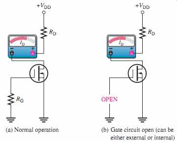
FIG. 55 An open fault in the gate circuit of a D-MOSFET causes no change
in ID.
In an E-MOSFET circuit with voltage-divider bias, an open R1 makes the gate voltage zero. This causes the transistor to be off and act like an open switch because a gate-to source threshold voltage greater than zero is required to turn the device on. This condition is illustrated in FIG. 56(a). If R2 opens, the gate is at +VDD and the channel resistance is very low so the device approximates a closed switch. The drain current is limited only by RD. This condition is illustrated in FIG. 56(b).
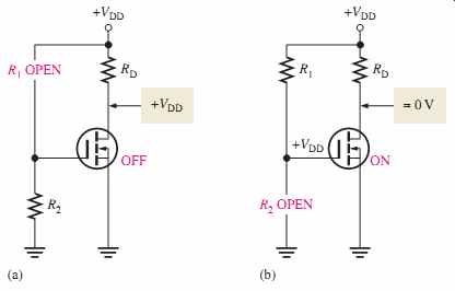
FIG. 56 Failures in an E-MOSFET circuit with voltage-divider bias.
SECTION 9 CHECKUP
1. In a self-biased JFET circuit, the drain voltage equals VDD. If the JFET is okay, what are other possible faults?
2. Why doesn't the drain current change when an open occurs in the gate circuit of a zero-biased D-MOSFET circuit?
3. If the gate of an E-MOSFET becomes shorted to ground in a circuit with voltage-divider bias, what is the drain voltage?
Application Activity: pH Sensor Circuit
This application involves electronic instrumentation in a waste water treatment facility.
The system controls the amount of acid and base reagent added to waste water in order to neutralize it. The diagram of the waste water neutralization pH system is shown in FIG. 57. The system measures and controls the pH of the water, which is a measure of the degree of acidity or alkalinity. The pH scale ranges from 0 for the strongest acids through 7 for neutral solutions and up to 14 for the strongest bases (caustics). Typically, the pH for waste water ranges from greater than 2 and less than 11. The pH of the water is measured by sensor probes at the inlets and outlets of the tanks. The processor and controller unit uses the inputs from the pH sensor circuits to adjust the amount of acid or base introduced into the neutralization tank. The pH should be 7 at the outlet of the smoothing tank.
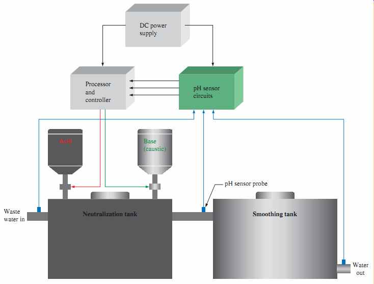
FIG. 57 Simplified waste water pH neutralization system.
Generally, waste water treatment is done in three steps as follows:
-- Primary treatment
Collecting, screening, and initial storage
-- Secondary treatment
Removal of solids and the majority of contaminants using filters, coagulation, flocculation, and membranes
- Tertiary treatment
- Polishing, pH adjustment, carbon treatment to remove taste and smells, disinfection, and temporary storage to allow the disinfecting agent to work In this application, we are focusing on the process of pH adjustment in the tertiary stage of treatment.
The Sensor Circuit
There are three identical pH sensor circuits, one for each of the inlet/outlets indicated in FIG. 57. The pH sensor produces a small voltage (mV) proportional to the pH of the water in which it is immersed. The pH sensor produces a negative voltage if the water is acidic, no voltage if it is neutral, and a positive voltage if it is basic. The sensor output goes to the gate of a MOSFET circuit, which amplifies the sensor voltage for processing by the digital controller.
FIG. 58 shows the pH sensor probe and a graph of output voltage versus pH.
FIG. 59 is the sensor circuit using a BF998 dual-gate n-channel MOSFET. A rheostat in the drain of the MOSFET is used to calibrate the circuit so that each of the three sensor circuits produce the same output voltage for a given value of pH.
1. Determine the approximate sensor voltage for a pH of 8.
2. Determine the approximate sensor voltage for a pH of 3.
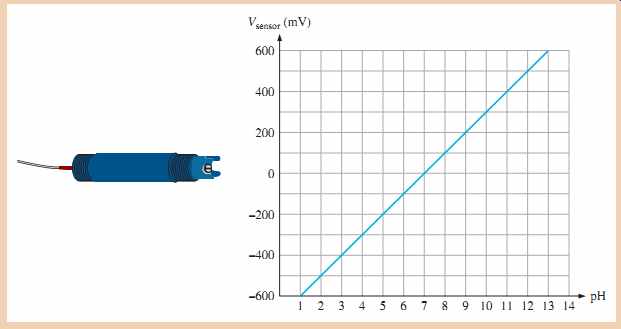
FIG. 58 pH sensor and graph of pH vs. output voltage.
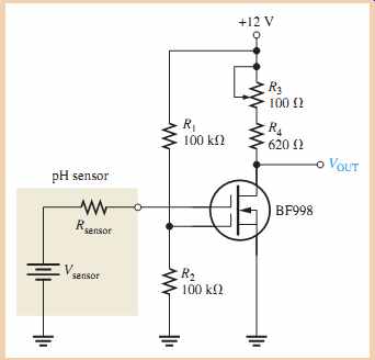
FIG. 59 pH sensor circuit.

FIG. 60 Partial datasheet for a BF998 MOSFET. Datasheet courtesy of Vishay
Intertechnology, Inc.
The partial datasheet for the BF998 D-MOSFET is shown in FIG. 60. In this application, the MOSFET is used as a dc amplifier. Recall that a D-MOSFET can operate with both positive and negative gate voltages, making it ideal for this particular application where the input voltage can have either polarity. The graph in FIG. 60 shows that the transconductance curve depends on the value of the voltage on the second gate which, in this particular design, is set at 6 V by the R1-R2 voltage divider. The input from the sensor is applied to the first gate.
3. What is the specified typical transconductance (trans-admittance) for the BF998?
4. If the drain-to-source voltage is 10 V, determine the maximum allowable drain current.
5. If one gate is biased to 1V, what is ID when the other gate is 0 V?
Simulation
The pH sensor circuit is simulated in Multisim, and the results for a series of sensor input voltages are shown in FIG. 61. The sensor is modeled as a dc source in series with an internal resistance. Notice that the output of the circuit increases as the sensor input decreases. Rheostat R3 is used to calibrate each of the three sensor circuits so that they have an identical output voltage for a given sensor input voltage.
6. If the output of the sensor circuit is 7 V, is the solution acidic, neutral, or basic (caustic)?
7. Plot a graph of V vs. pH for each measurement in FIG. 61.
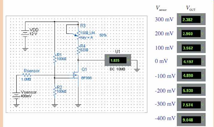
FIG. 61 Simulation results for the pH sensor circuit.
Prototyping and Testing
Now that the circuit has been simulated, the prototype circuit is constructed and tested. A dc voltage source can be used to provide the sensor input voltages. After the circuit is successfully tested on a protoboard, it is ready to be finalized on a printed circuit board.
Circuit Board
The pH sensor circuits are implemented on a printed circuit board as shown in FIG. 62.
Each circuit monitors one of the three pH sensors in the system. Note that a single voltage divider provides -6 V to the second gate of each transistor.
8. Check the printed circuit board for correctness by comparing with the schematic in FIG. 59.
9. Identify the connections on the back side of the board.
10. Label each input and output pin according to function.
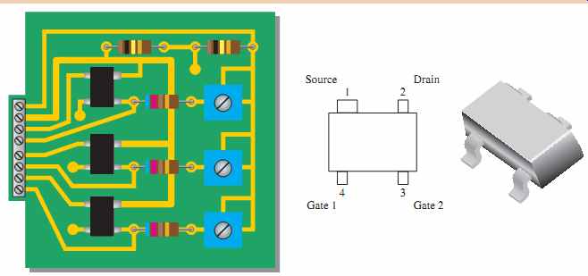
FIG. 62 pH sensor circuit board.
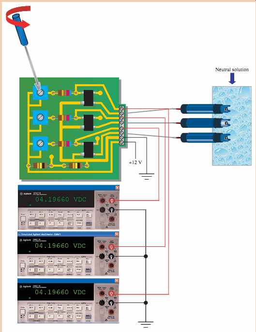
FIG. 63 Calibration and testing of the pH sensor circuits.
Calibration and Testing
The first step is to calibrate each of the three circuits for a pH of 7. Using a known neutral test solution in a container into which the sensors are placed, the rheostat is adjusted (if necessary) to produce the same output voltage for each circuit. In this case it is 4.197 V, as shown in FIG. 63.
The next step is to replace the neutral solution with one that has an acidity with a known pH. All the circuits should produce the same voltage within a specified tolerance. Finally, using a basic solution with a known pH, measure the output voltages. Again, they should all agree.
SUMMARY OF FIELD-EFFECT TRANSISTORS
JFETS
¦ Gate-source pn junction must be reverse-biased.
¦ VGS controls ID.
¦ Value of VDS at which ID becomes constant is the pinch-off voltage.
¦ Value of VGS at which ID becomes zero is the cutoff voltage, VGS(off ).
¦ IDSS is drain current when VGS=0.
¦ Transfer characteristic:
E-MOSFETS
Operates in enhancement mode only.
¦ VGS must exceed VGS(th).
¦ Enhancement mode:
n channel: VGS positive p channel: VGS negative
¦ VGS controls ID.
¦ Value of VGS at which ID begins is the threshold voltage, VGS(th).
¦ Transfer characteristic:
¦ K in formula can be calculated by substituting datasheet values ID(on) for ID and VGS at which ID(on) is specified for VGS.
ID = K(VGS - VGS(th))^2
D-MOSFETS
Can be operated in either depletion or enhancement modes. VGS can be either polarity when biased at VGS = 0 V.
¦ Depletion mode:
n channel: VGS negative p channel: VGS positive
¦ Enhancement mode:
n channel: VGS positive p channel: VGS negative
¦ VGS controls ID.
¦ Value of VGS at which ID becomes zero is the cutoff voltage, VGS(off ).
¦ IDSS is drain current when VGS = 0.
Transfer characteristic:
IGBT
¦ Voltage controlled like a MOSFET
¦ Output characteristics like a BJT
¦ Three terminals: gate, collector, emitter
FET BIASING (Voltage polarities and current directions reverse for p channel)
SUMMARY
Section 1
-- Field-effect transistors are unipolar devices (one-charge carrier).
-- The three FET terminals are source, drain, and gate.
-- The JFET operates with a reverse-biased pn junction (gate-to-source).
-- The high input resistance of a JFET is due to the reverse-biased gate-source junction.
-- Reverse bias of a JFET produces a depletion region within the channel, thus increasing channel resistance.
Section 2
-- For an n-channel JFET, VGS can vary from zero negatively to cutoff, VGS(off). For a p-channel JFET, VGS can vary from zero positively to VGS(off ).
-- IDSS is the constant drain current when VGS = 0. This is true for both JFETs and D-MOSFETs.
-- A FET is called a square-law device because of the relationship of ID to the square of a term containing VGS.
Section 3
-- Midpoint bias for a JFET is ID = IDSS 2, obtained by setting VGS VGS(off ) 3.4.
-- The Q-point in a JFET with voltage-divider bias is more stable than in a self-biased JFET.
-- Current-source bias increases the stability of a self-biased JFET.
Section 4
-- A JFET used as a variable resistor is biased in the ohmic region.
-- To bias in the ohmic region, ID must be much smaller than IDSS.
-- The gate voltage controls RDS in the ohmic region.
-- When a JFET is biased at the origin (VDS = 0, ID = 0), the ac channel resistance is controlled by the gate voltage.
Section 5
-- MOSFETs differ from JFETs in that the gate of a MOSFET is insulated from the channel by an SiO2 layer, whereas the gate and channel in a JFET are separated by a pn junction.
-- A depletion MOSFET (D-MOSFET) can operate with a zero, positive, or negative gate-to source voltage.
-- The D-MOSFET has a physical channel between the drain and source.
-- For an n-channel D-MOSFET, negative values of VGS produce the depletion mode and positive values produce the enhancement mode.
-- The enhancement MOSFET (E-MOSFET) has no physical channel.
-- Unlike JFETs and D-MOSFETs, the E-MOSFET cannot operate with VGS = 0 V.
-- A channel is induced in an E-MOSFET by the application of a VGS greater than the threshold value, VGS(th).
Section 6
-- An E-MOSFET has no IDSS parameter. It is extremely small, if specified (ideally 0).
-- An n-channel E-MOSFET has a positive VGS(th). A p-channel E-MOSFET has a negative VGS(th).
-- The transfer characteristic curve for a D-MOSFET intersects the vertical ID axis.
-- The transfer characteristic curve for an E-MOSFET does not intersect the ID axis.
-- All MOS devices are subject to damage from electrostatic discharge (ESD).
Section 7
-- Midpoint bias for a D-MOSFET is ID = IDSS obtained by setting VGS = 0.
-- The gate of a zero-biased D-MOSFET is at 0 V due to a large resistor to ground.
-- An E-MOSFET must have a VGS greater than the threshold value.
Section 8
-- The insulated-gate bipolar transistor (IGBT) combines the input characteristics of a MOSFET with the output characteristics of a BJT.
-- The IGBT has three terminals: emitter, gate, and collector.
-- IGBTs are used in high-voltage switching applications.
Section 9
-- An open gate is hard to detect in a zero-biased D-MOSFET because the gate is normally at 0 V; however, erratic behavior may occur.
-- An open gate is easy to detect in an E-MOSFET because the gate is normally at a voltage other than 0 V.
TERMS
Depletion In a MOSFET, the process of removing or depleting the channel of charge carriers and thus decreasing the channel conductivity.
Drain One of the three terminals of a FET analogous to the collector of a BJT.
Enhancement In a MOSFET, the process of creating a channel or increasing the conductivity of the channel by the addition of charge carriers.
Gate One of the three terminals of a FET analogous to the base of a BJT.
IGBT Insulated-gate bipolar transistor; a device that combines features of the MOSFET and the BJT and used mainly for high-voltage switching applications.
JFET Junction field-effect transistor; one of two major types of field-effect transistors.
MOSFET Metal oxide semiconductor field-effect transistor; one of two major types of FETs; sometimes called IGFET for insulated-gate FET.
Ohmic region The portion of the FET characteristic curve lying below pinch-off in which Ohm's law applies.
Pinch-off voltage The value of the drain-to-source voltage of a FET at which the drain current becomes constant when the gate-to-source voltage is zero.
Source One of the three terminals of a FET analogous to the emitter of a BJT.
Transconductance (gm) The ratio of a change in drain current to a change in gate-to-source volt age in a FET.
KEY FORMULAS
[…]
TRUE/FALSE QUIZ
1. The JFET always operates with a reverse-biased gate-to-source pn junction.
2. The channel resistance of a JFET is a constant.
3. The gate-to-source voltage of an n-channel JFET must be negative.
4. ID becomes zero at the pinch-off voltage.
5. VGS has no effect on ID.
6. VGS(off ) and VP are always equal in magnitude but opposite in polarity.
7. The JFET is a square-law device because of the mathematical expression of its transfer characteristic curve.
8. Forward transconductance is the change in drain voltage for a given change in gate voltage.
9. The parameters gm and yfs are the same.
10. The D-MOSFET can be operated in two modes.
11. An E-MOSFET operates in the depletion mode.
12. A D-MOSFET has a physical channel and an E-MOSFET has an induced channel.
13. ESD means electronic semiconductor device.
14. MOSFETs must be handled with care.
CIRCUIT-ACTION QUIZ:
1. If the drain current in FIG. 17 is increased, VDS will (a) increase (b) decrease (c) not change
2. If the drain current in FIG. 17 is increased, VGS will (a) increase (b) decrease (c) not change
3. If the value of RD in FIG. 24 is increased, ID will (a) increase (b) decrease (c) not change
4. If the value of R2 in FIG. 24 is decreased, VG will (a) increase (b) decrease (c) not change
5. If VGS in FIG. 47 is increased, ID will (a) increase (b) decrease (c) not change
6. If R2 in FIG. 47 opens, VGS will (a) increase (b) decrease (c) not change
7. If the value of RG in FIG. 50 is increased, VG will (a) increase (b) decrease (c) not change
8. If the value of IDSS in FIG. 50 is increased, VDS will (a) increase (b) decrease (c) not change
SELF-TEST
Section 1
1. The JFET is (a) a unipolar device (b) a voltage-controlled device (c) a current-controlled device (d) answers (a) and (c) (e) answers (a) and (b)
2. The channel of a JFET is between the (a) gate and drain (b) drain and source (c) gate and source (d) input and output
3. A JFET always operates with (a) the gate-to-source pn junction reverse-biased (b) the gate-to-source pn junction forward-biased (c) the drain connected to ground (d) the gate connected to the source Section 2 4. For VGS = 0 V, the drain current becomes constant when VDS exceeds (a) cutoff (b) VDD (c) VP (d) 0 V
5. The constant-current region of a FET lies between (a) cutoff and saturation (b) cutoff and pinch-off (c) 0 and IDSS (d) pinch-off and breakdown
6. IDSS is (a) the drain current with the source shorted (b) the drain current at cutoff (c) the maximum possible drain current (d) the midpoint drain current.
7. Drain current in the constant-current region increases when (a) the gate-to-source bias voltage decreases (b) the gate-to-source bias voltage increases (c) the drain-to-source voltage increases (d) the drain-to-source voltage decreases.
8. In a certain FET circuit, VGS= 0 V, VDD = 15 V, IDSS = 15 mA, and If RD is decreased to (a) 19.5 mA (b) 10.5 mA (c) 15 mA (d) 1 mA
9. At cutoff, the JFET channel is (a) at its widest point (b) completely closed by the depletion region (c) extremely narrow (d) reverse-biased
10. A certain JFET datasheet gives The pinch-off voltage, VP, (a) cannot be determined (b) is (c) depends on VGS (d) is -4 V
11. The JFET in Question 10 (a) is an n channel (b) is a p channel (c) can be either
12. For a certain JFET, IGSS = 10 nA at VGS = 10 V. The input resistance is (a) (b) (c) (d) Section 3
13. For a certain p-channel JFET, VGS(off ) = 8 V. The value of VGS for an approximate midpoint bias is (a) 4 V (b) 0 V (c) 1.25 V (d) 2.34 V
14. In a self-biased JFET, the gate is at (a) a positive voltage (b) 0 V (c) a negative voltage (d) ground Section 4
15. The drain-to-source resistance in the ohmic region depends on (a) VGS (b) the Q-point values (c) the slope of the curve at the Q-point (d) all of these
16. To be used as a variable resistor, a JFET must be (a) an n-channel device (b) a p-channel device (c) biased in the ohmic region (d) biased in saturation
17. When a JFET is biased at the origin, the ac channel resistance is determined by (a) the Q-point values (b) VGS (c) the transconductance (d) answers (b) and (c) 1000 M-OHM 1000 M-OHM 1 M-OHM 100 M-OHM -4V VGS(off ) =-4V.
330 OHM, IDSS is RD = 470 OHM.
Section 5
18. A MOSFET differs from a JFET mainly because (a) of the power rating (b) the MOSFET has two gates (c) the JFET has a pn junction (d) MOSFETs do not have a physical channel
19. A D-MOSFET operates in (a) the depletion mode only (b) the enhancement mode only (c) the ohmic region only (d) both the depletion and enhancement modes Section 6
20. An n-channel D-MOSFET with a positive VGS is operating in (a) the depletion mode (b) the enhancement mode (c) cutoff (d) saturation
21. A certain p-channel E-MOSFET has a If VGS = 0 V, the drain current is (a) 0 A (b) ID(on) (c) maximum (d) IDSS
22. In an E-MOSFET, there is no drain current until VGS (a) reaches VGS(th) (b) is positive (c) is negative (d) equals 0 V
23. All MOS devices are subject to damage from (a) excessive heat (b) electrostatic discharge (c) excessive voltage (d) all of these Section 7
24. A certain D-MOSFET is biased at VGS = 0 V. Its datasheet specifies IDSS = 20 mA and The value of the drain current (a) is 0 A (b) cannot be determined (c) is 20 mA
Section 8
25. An IGBT is generally used in (a) low-power applications (b) rf applications (c) high-voltage applications (d) low-current applications
PROBLEMS
BASIC PROBLEMS
Section 1 The JFET
1. The VGS of a p-channel JFET is increased from 1 V to 3 V.
(a) Does the depletion region narrow or widen? (b) Does the resistance of the channel increase or decrease?
2. Why must the gate-to-source voltage of an n-channel JFET always be either 0 or negative?
3. Draw the schematic diagrams for a p-channel and an n-channel JFET. Label the terminals.
VGS(off) =-5V.
VGS(th) =-2V.
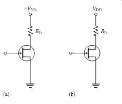
FIG. 64
4. Show how to connect bias voltages between the gate and source of the JFETs in FIG. 64.
+VDD -VDD
Section 2
JFET Characteristics and Parameters
5. A JFET has a specified pinch-off voltage of 5 V. When VGS = 0, what is VDS at the point where the drain current becomes constant?
6. A certain n-channel JFET is biased such that What is the value of VGS(off) if VP is specified to be 6 V? Is the device on?
7. A certain JFET datasheet gives When VGS = 0, what is ID for values of VDS above pinch off? VDD = 15 V.
8. A certain p-channel JFET has a VGS(off) = 6 V. What is ID when VGS = 8 V?
9. The JFET in FIG. 65 has a Assume that you increase the supply voltage, VDD, beginning at zero until the ammeter reaches a steady value. What does the voltmeter read at this point? VGS(off) =-4V.
VGS(off) =-8 V and IDSS = 10 mA.
VGS =-2V.
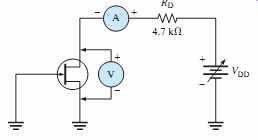
FIG. 65
10. The following parameters are obtained from a certain JFET datasheet: Determine the values of ID for each value of VGS ranging from 0 V to in 1 V steps. Plot the transfer characteristic curve from these data.
11. For the JFET in Problem 10, what value of VGS is required to set up a drain current of 2.25 mA? 12. For a particular JFET, What is gm when given that 13. Determine the forward transconductance of a JFET biased at From the datasheet, VGS =-2V.
VGS(off ) =-8V? VGS =-4V, gm0 = 3200 mS.
-8V IDSS = 5 mA.
VGS(off) =-8 V and at VGS = 0 V. Also determine the forward transfer conductance,
14. A p-channel JFET datasheet shows that IGSS = 5nAat VGS= 10 V. Determine the input resistance.
15. Using Equation 1, plot the transfer characteristic curve for a JFET with IDSS = 8 mA and Use at least four points.
Section 3
JFET Biasing
16. An n-channel self-biased JFET has a drain current of 12 mA and a source resistor. What is the value of VGS? 100 OHM VGS(off ) =-5V.
gfs.
VGS(off ) =-7 V and gm = 2000 mS
17. Determine the value of RS required for a self-biased JFET to produce a VGS of when ID = 5 mA.
18. Determine the value of RS required for a self-biased JFET to produce ID = 2.5 mA when
19. IDSS = 20 mA and for a particular JFET.
(a) What is ID when VGS = 0 V? (b) What is ID when VGS = VGS(off)? (c) If VGS is increased from does ID increase or decrease?
20. For each circuit in FIG. 66, determine VDS and VGS.
-4Vto -1V, VGS(off) =-6V VGS =-3V.
-4V
21. Using the curve in FIG. 67, determine the value of RS required for a 9.5 mA drain current.
22. Set up a midpoint bias for a JFET with IDSS = 14 mA and Use a 24 V dc source as the supply voltage. Show the circuit and resistor values. Indicate the values of ID, VGS, and VDS.
23. Determine the total input resistance in FIG. 68. IGSS = 20 nA at VGS =-10 V.
VGS(off) =-10 V.
FIG. 66 Multisim file circuits are identified with a logo and are in the Problems folder on the companion website. Filenames correspond to figure numbers (e.g., F08-66).
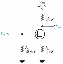
FIG. 68
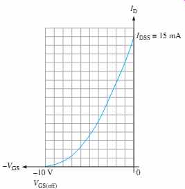
FIG. 67
24. Graphically determine the Q-point for the circuit in FIG. 69(a) using the transfer characteristic curve in FIG. 69(b).
25. Find the Q-point for the p-channel JFET circuit in FIG. 70.
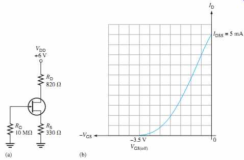
FIG. 69
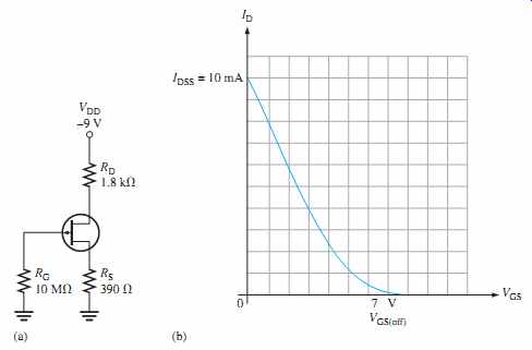
FIG. 70
26. Given that the drain-to-ground voltage in FIG. 71 is 5 V, determine the Q-point of the circuit.
27. Find the Q-point values for the JFET with voltage-divider bias in FIG. 72.
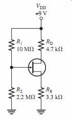
FIG. 71
FIG. 72
Section 4
The Ohmic Region
28. A certain JFET is biased in the ohmic region at VDS = 0.8 V and ID = 0.20 mA. What is the drain-to-source resistance?
29. The Q-point of a JFET is varied from VDS = 0.4 V and ID = 0.15 mA to VDS = 0.6 V and ID = 0.45 mA. Determine the range of RDS values.
30. Determine the transconductance of a JFET biased at the origin given that gm0 = 1.5 mS,
31. Determine the ac drain-to-source resistance of the JFET in Problem 30.
Section 5
The MOSFET
32. Draw the schematic symbols for n-channel and p-channel E-MOSFETs and D-MOSFETs.
Label the terminals.
33. In what mode is an n-channel D-MOSFET with a positive VGS operating?
34. Describe the basic difference between an E-MOSFET and a D-MOSFET.
35. Explain why both types of MOSFETs have an extremely high input resistance at the gate.
Section 6
MOSFET Characteristics and Parameters
36. The datasheet for an E-MOSFET reveals that ID(on) _ 10 mA at Find ID when 37. Determine IDSS, given ID = 3 mA, VGS =-2 V, and VGS(off ) =-10 V.
VGS =-6V. VGS(th) =-3V.
VGS =-12 V and VGS =-1 V, and VGS(off ) =-3.5 V.
38. The datasheet for a certain D-MOSFET gives (a) Is this device p channel or n channel? (b) Determine ID for values of VGS ranging from in increments of 1 V.
(c) Plot the transfer characteristic curve using the data from part (b).
Section 7
MOSFET Biasing
39. Determine in which mode (depletion, enhancement or neither) each D-MOSFET in FIG. 73 is biased.
-5Vto +5V VGS(off ) =-5 V and IDSS = 8 mA.
40. Each E-MOSFET in FIG. 74 has a VGS(th) of -5 V or depending on whether it is an n-channel or a p-channel device. Determine whether each MOSFET is on or off.
-5V,
+10 V -25 V
41. Determine VDS for each circuit in FIG. 75. IDSS = 8 mA.
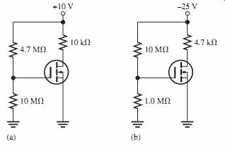
FIG. 74
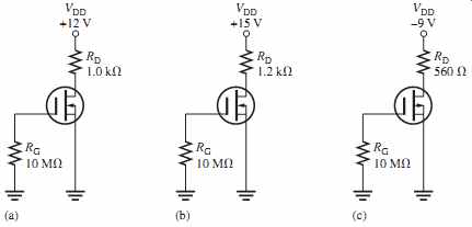
FIG. 75
42. Find VGS and VDS for the E-MOSFETs in FIG. 76. Datasheet information is listed with each circuit.
43. Based on the VGS measurements, determine the drain current and drain-to-source voltage for each circuit in FIG. 77.
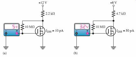
FIG. 77
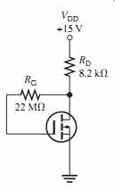
FIG. 78
44. Determine the actual gate-to-source voltage in FIG. 78 by taking into account the gate leakage current, IGSS. Assume that IGSS is 50 pA and ID is 1 mA under the existing bias conditions.
Section 8
The IGBT 45. Explain why the IGBT has a very high input resistance.
46. Explain how an excessive collector current can produce a latch-up condition in an IGBT.
Section 9 Troubleshooting
47. The current reading in FIG. 66(a) suddenly goes to zero. What are the possible faults?
48. The current reading in FIG. 66(b) suddenly jumps to approximately 16 mA. What are the possible faults?
49. If the supply voltage in FIG. 66(c) is changed to what would you see on the ammeter?
50. You measure at the drain of the MOSFET in FIG. 74(a). The transistor checks good and the ground connections are okay. What can be the problem?
51. You measure approximately 0 V at the drain of the MOSFET in FIG. 74(b). You can find no shorts and the transistor checks good. What is the most likely problem?
APPLICATION ACTIVITY
PROBLEMS
52. Refer to FIG. 58 and determine the sensor voltage for each of the following pH values.
(a) 2 (b) 5 (c) 7 (d) 11
53. Referring to the transconductance curves for the BF998 in FIG. 79, determine the change in ID when the bias on the second gate is changed from 6 V to 1 V and VG1S is 0.0 V. Each curve represents a different V value.
+10 V
-20 V,
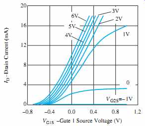
FIG. 79 Transconductance curves for BF998.
54. Refer to FIG. 61 and plot the transconductance curve (ID vs. VG1S).
55. Refer to FIG. 79. Determine the output voltage of the circuit in FIG. 61 if VG1S = Vsensor = 0 V and R2 is changed to:
DATASHEET PROBLEMS
56. What type of FET is the 2N5457?
57. Referring to the datasheet in FIG. 14, determine the following:
(a) Minimum VGS(off) for the 2N5457.
(b) Maximum drain-to-source voltage for the 2N5457.
(c) Maximum power dissipation for the 2N5458 at an ambient temperature of 25°C.
(d) Maximum reverse gate-to-source voltage for the 2N5459.
58. Referring to FIG. 14, determine the maximum power dissipation for a 2N5457 at an ambient temperature of 65°C.
59. Referring to FIG. 14, determine the minimum gm0 for the 2N5459 at a frequency of 1 kHz.
60. Referring to FIG. 14, what is the typical drain current in a 2N5459 for VGS = 0 V?
61. Referring to the 2N3796 datasheet in FIG. 80, determine the drain current for VGS = 0 V.
50 kOHM.
FIG. 80 Partial datasheet for the 2N3797 D-MOSFET.
62. Referring to FIG. 80, what is the drain current for a 2N3796 when VGS =6 V?
63. Referring to the datasheet in FIG. 80, determine ID in a 2N3797 when VGS = -3 V.
Determine ID when VGS =-2V.
64. Referring to FIG. 80, how much does the maximum forward transconductance of a 2N3796 change over a range of signal frequencies from 1 kHz to 1 MHz?
65. Referring to FIG. 80, determine the typical value of gate-to-source voltage at which the 2N3796 will go into cutoff.
ADVANCED PROBLEMS
66. Find VDS and VGS in FIG. 81 using minimum datasheet values.
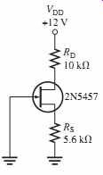
FIG. 81
67. Determine the maximum ID and VGS for the circuit in FIG. 82.
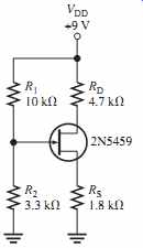
FIG. 82
68. Determine the range of possible Q-point values from minimum to maximum for the circuit in FIG. 81.
69. Find the drain-to-source voltage for the pH sensor circuit in FIG. 59 when a pH of 5 is measured. Assume the rheostat is set to produce 4 V at the drain when a pH of 7 is measured.
70. Design a MOSFET circuit with zero bias using a 2N3797 that operates from a -9 V dc supply and produces a VDS of 4.5 V. The maximum current drawn from the source is to be 1 mA.
71. Design a circuit using an n-channel E-MOSFET with the following datasheet specifications: ID(on) = 500 mA@VGS = 10 V and VGS(th) = 1V. Use a -12 V dc supply voltage with voltage-divider bias. The voltage at the drain with respect to ground is to be -8 V. The maxi mum current from the supply is to be 20 mA.