AMAZON multi-meters discounts AMAZON oscilloscope discounts
OUTLINE
1. The Common-Source Amplifier (this page; see below)
2. The Common-Drain Amplifier (this page; see below)
3. The Common-Gate Amplifier (this page; see below)
4 The Class D Amplifier (this page; see below)
5. MOSFET Analog Switching (this page; see below)
GOALS:
- Explain and analyze the operation of common-source FET amplifiers
- Explain and analyze the operation of common-drain FET amplifiers
- Explain and analyze the operation of common-gate FET amplifiers
- Discuss the operation of a class D amplifier
- Describe how MOSFETs can be used in analog switching applications
- Describe how MOSFETs are used in digital switching applications
- Troubleshoot FET amplifiers
TERMINOLOGY
- Common-source
- Common-drain
- Source-follower
- Common-gate
- Class D amplifier
- Pulse-width modulation
- Analog switch
- CMOS
APPLICATION ACTIVITY PREVIEW
A JFET common-source amplifier and a common-gate amplifier are combined in a cascode arrangement for an active antenna. Cascode amplifiers are often used for RF (radio frequency) applications to achieve improved high-frequency performance. In this application, the cascode amplifier pro vides a high resistance input for a whip antenna, as well as high gain to amplify extremely small antenna signals.
INTRODUCTION
Because of their extremely high input resistance and low noise, FET amplifiers are a good choice for certain applications, such as amplifying low-level signals in the first stage of a communication receiver. FETs also have the advantage in certain power amplifiers and in switching circuits because biasing is simple and more efficient. The standard amplifier configurations are common-source (CS), common-drain (CD) and common-base (CB), which are analogous to CE, CC, and CB configurations of BJTs.
FETs can be used in any of the amplifier types introduced earlier (class A, class B, and class C). In some cases, the FET circuit will perform better; in other cases, the BJT circuit is superior because BJTs have higher gain and better linearity.
Another type of amplifier (class D) is introduced in this section because FETs are always superior to BJTs in class D and you will rarely see BJTs used in class D. The class D amplifier is a switching amplifier that is normally either in cutoff or saturation. It is used in analog power amplifiers with a circuit called a pulse-width modulator, introduced in Section 4.
FETs are superior to BJTs in nearly all switching applications. Various switching circuits-analog switches, analog multiplexers, and switched capacitors-are discussed. In addition, common digital switching circuits are introduced using CMOS (complementary MOS).
1. THE COMMON-SOURCE AMPLIFIER
When used in amplifier applications, the FET has an important advantage compared to the BJT due to the FET's extremely high input impedance. Disadvantages, however, include higher distortion and lower gain. The particular application will usually deter mine which type of transistor is best suited. The common-source (CS) amplifier is comparable to the common-emitter BJT amplifier that you studied in section 6.
GOALS:
- Explain and analyze the operation of common-source FET amplifiers
- Discuss and analyze the FET ac model
- Describe and analyze common-source JFET amplifier operation
- Perform dc analysis of a JFET amplifier
- Use the graphical approach
--- Use the mathematical approach
- Use the TI-89 calculator * (if available)
- Discuss and analyze the ac equivalent circuit of a JFET amplifier
- Determine the signal voltage at the gate
---Determine the voltage gain
- Explain the effect of an ac load on the voltage gain
- Discuss phase inversion
- Determine amplifier input resistance
- Describe and analyze D-MOSFET amplifier operation
- Describe and analyze E-MOSFET amplifier operation
- Determine input resistance
FET AC Model
An equivalent FET model is shown in FIG. 1. In part (a), the internal resistance, r’ gs, appears between the gate and source, and a current source equal to gm Vgs appears between the drain and source. Also, the internal drain-to-source resistance, r’ ds, is included. In part (b), a simplified ideal model is shown. The resistance, r’ gs, is assumed to be extremely large so that an open circuit between the gate and source can be assumed. Also, r' ds is assumed large enough to neglect.
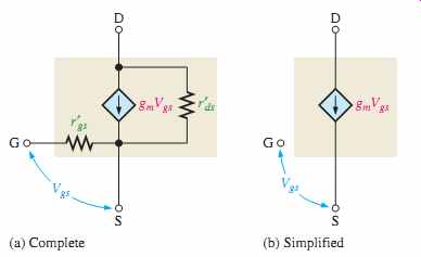
FIG. 1 Internal FET equivalent circuits.
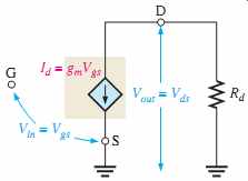
FIG. 2 Simplified FET equivalent circuit with an external ac drain
resistance.
An ideal FET circuit model with an external ac drain resistance is shown in FIG. 2.
The ac voltage gain of this circuit is Vout/ Vin, where Vin=Vgs and Vout = Vds . The voltage gain expression is, therefore,
Av = Vds / Vgs
From the equivalent circuit,
Equation 1
JFET Amplifier Operation
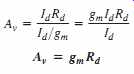
A common-source JFET amplifier is one in which the ac input signal is applied to the gate and the ac output signal is taken from the drain. The source terminal is common to both the input and output signal. A common-source amplifier either has no source resistor or has a bypassed source resistor, so the source is connected to ac ground. A self-biased common-source n-channel JFET amplifier with an ac source capacitively coupled to the gate is shown in FIG. 3(a). The resistor, RG, serves two purposes: It keeps the gate at approximately 0 V dc (because IGSS is extremely small), and its large value (usually several megohms) prevents loading of the ac signal source. A bias voltage is produced by the drop across RS. The bypass capacitor, C2, keeps the source of the JFET at ac ground.
FIG. 3 JFET common-source amplifier.
The input signal voltage causes the gate-to-source voltage to swing above and below its Q-point value (VGSQ), causing a corresponding swing in drain current. As the drain current increases, the voltage drop across RD also increases, causing the drain voltage to decrease.
The drain current swings above and below its Q-point value in phase with the gate-to-source voltage. The drain-to-source voltage swings above and below its Q-point value (VDSQ) and is 180° out of phase with the gate-to-source voltage, as illustrated in FIG. 3(b).
A Graphical Picture---The operation just described for an n-channel JFET is illustrated graphically on both the transfer characteristic curve and the drain characteristic curve in FIG. 4. Part (a) shows how a sinusoidal variation, Vgs, produces a corresponding sinusoidal variation in Id. As Vgs swings from its Q-point value to a more negative value, Id decreases from its Q-point value. As Vgs swings to a less negative value, Id increases. FIG. 4(b) shows a view of the same operation using the drain curves. The signal at the gate drives the drain current above and below the Q-point on the load line, as indicated by the arrows.
Lines projected from the peaks of the gate voltage across to the ID axis and down to the VDS axis indicate the peak-to-peak variations of the drain current and drain-to-source voltage, as shown. Because the transfer characteristic curve is nonlinear, the output will have some distortion. This can be minimized if the signal swings over a limited portion of the load line.
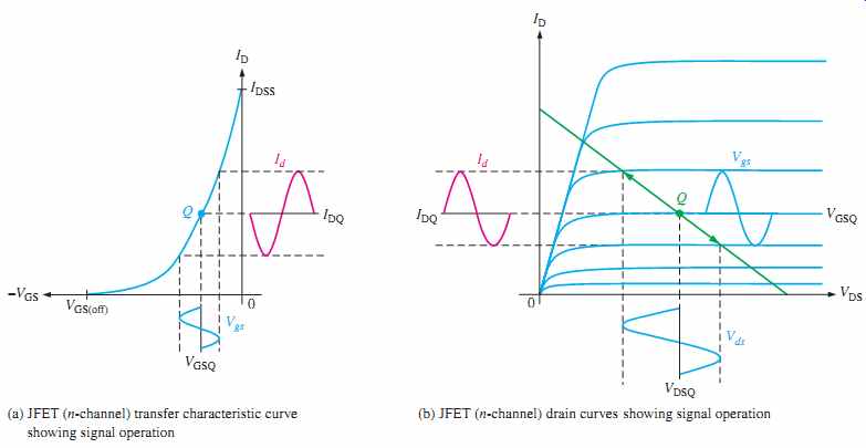
FIG. 4
JFET characteristic curves. (a) JFET (n-channel) transfer characteristic
curve showing signal operation; (b) JFET (n-channel) drain curves showing
signal operation
DC Analysis
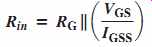
The first step in analyzing a JFET amplifier is to determine the dc conditions including ID and VS. ID determines the Q-point for an amplifier and enables you to calculate VD, so it is useful to determine its value. It can be found either graphically or mathematically. The graphical approach, introduced in section 8 using the transconductance curve, will be applied to an amplifier here. The same result can be obtained by expanding Equation 1, which is the mathematical description of the transconductance curve. The amplifier shown in FIG. 5 will be used to illustrate both approaches. To simplify the dc analysis, the equivalent circuit is shown in FIG. 6; capacitors appear open to dc, so they are removed.
Graphical Approach---Recall from Section 8-2 that the JFET universal transfer characteristic (transconductance curve) illustrates the relationship between the output current and the input voltage. The endpoints of the transconductance curve are at IDSS and VGS(off). A dc graphical solution is done by plotting the load line (for the self-biased case shown) on the same plot and reading the values of VGS and ID at the intersection of these plots (Q-point).
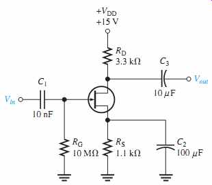
FIG. 5 JFET common-source amplifier.
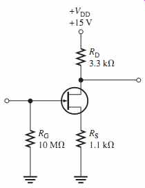
FIG. 6 DC equivalent for the amplifier in FIG. 5.
Mathematical Approach---The mathematical approach is more tedious than the graphical approach because it involves expanding the equation into quadratic form and solving the quadratic equation. To determine ID mathematically from the known quantities, substitute VGS = IDRS into Equation 1. The result is shown as Equation 2, which has ID on both sides. Isolating ID requires the solution of the quadratic form. A much easier approach is to enter Equation 2 into a graphing calculator such as the TI-89. The steps for determining ID using the TI-89 are given in Example 3.
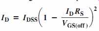
Equation 2
AC Equivalent Circuit
To analyze the signal operation of the amplifier in FIG. 5, develop an ac equivalent circuit as follows. Replace the capacitors by effective shorts, based on the simplifying assumption that XC =_ 0 at the signal frequency. Replace the dc source by a ground, based on the assumption that the voltage source has a zero internal resistance. The VDD terminal is at a zero-volt ac potential and therefore acts as an ac ground.
The ac equivalent circuit is shown in FIG. 8(a). Notice that the +VDD end of Rd and the source terminal are both effectively at ac ground. Recall that in ac analysis, the ac ground and the actual circuit ground are treated as the same point.
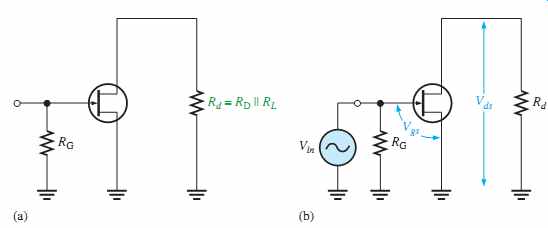
FIG. 8 AC equivalent for the amplifier in FIG. 5.
Signal Voltage at the Gate---An ac voltage source is shown connected to the input in FIG. 8(b). Since the input resistance to a JFET is extremely high, practically all of the input voltage from the signal source appears at the gate with very little voltage dropped across the internal source resistance.
Vgs = Vin
Voltage Gain---The expression for JFET voltage gain that was given in Equation 1 applies to the common-source amplifier.
Equation 3 Av = gm Rd
The output signal voltage Vds at the drain is
Vout = Vds = Av Vgs
or Vout = gm Rd Vin
where Rd = RD 7 RL and Vin = Vgs.
Effect of an AC Load on Voltage Gain
When a load is connected to an amplifier's output through a coupling capacitor, as shown in FIG. 10(a), the ac drain resistance is effectively RD in parallel with RL because the upper end of RD is at ac ground. The ac equivalent circuit is shown in FIG. 10(b). The total ac drain resistance is
Rd = RDRL / RD + RL
The effect of RL is to reduce the unloaded voltage gain, as Example 5 illustrates.
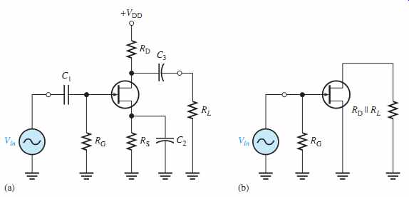
FIG. 10 JFET amplifier and its ac equivalent.
Phase Inversion
The output voltage (at the drain) is out of phase with the input voltage (at the gate).
The phase inversion can be designated by a negative voltage gain , -Av. Recall that the common-emitter BJT amplifier also exhibited a phase inversion.
Input Resistance
Because the input to a common-source amplifier is 180° at the gate, the input resistance is extremely high. Ideally, it approaches infinity and can be neglected. As you know, the high input resistance is produced by the reverse-biased pn junction in a JFET and by the insulated gate structure in a MOSFET. The actual input resistance seen by the signal source is the gate-to-ground resistor, RG, in parallel with the FET's input resistance, VGS / IGSS. The reverse leakage current, IGSS, is typically given on the datasheet for a specific value of VGS so that the input resistance of the device can be calculated.
Equation 4
Since VGS>IGSS the term is typically much larger than RG, the input resistance is very close to the value of RG, as Example 6 shows.
D-MOSFET Amplifier Operation
A zero-biased common-source n-channel D-MOSFET with an ac source capacitively coupled to the gate is shown in FIG. 12. The gate is at approximately 0 V dc and the source terminal is at ground, thus making VGS = 0 V.
FIG. 12 Zero-biased D-MOSFET common source amplifier.
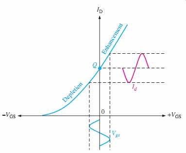
FIG. 13 Depletion-enhancement operation of D-MOSFET shown on transfer
characteristic curve.
The signal voltage causes Vgs to swing above and below its zero value, producing a swing in Id, as shown in FIG. 13. The negative swing in Vgs produces the depletion mode, and Id decreases. The positive swing in Vgs produces the enhancement mode, and Id increases. Note that the enhancement mode is to the right of the vertical axis (VGS = 0), and the depletion mode is to the left. The dc analysis of this amplifier is somewhat easier than for a JFET because
ID = IDSS at VGS = 0.
Once ID is known, the analysis involves calculating only VD.
VD = VDD - ID RD
The ac analysis is the same as for the JFET amplifier.
E-MOSFET Amplifier Operation
A common-source n-channel E-MOSFET with voltage-divider bias with an ac source capacitively coupled to the gate is shown in FIG. 14. The gate is biased with a positive voltage such that VGS 7 VGS(th).
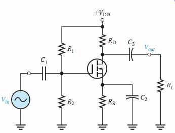
FIG. 14 Common-source E-MOSFET amplifier with voltage-divider bias.
As with the JFET and D-MOSFET, the signal voltage produces a swing in Vgs above and below its Q-point value, VGSQ. This, in turn, causes a swing in Id above and below its Q-point value, IDQ, as illustrated in FIG. 15. Operation is entirely in the enhancement mode.
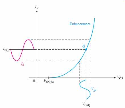
FIG. 15 E-MOSFET (n-channel) operation shown on transfer characteristic
curve.
The circuit in FIG. 14 uses voltage-divider bias to achieve a VGS above threshold.
The general dc analysis proceeds as follows using the E-MOSFET characteristic equation (Equation 4) to solve for ID.

The voltage gain expression is the same as for the JFET and D-MOSFET circuits. The ac input resistance is:
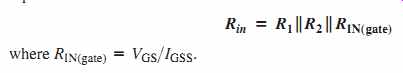
Equation 5
Section 1 CHECKUP
1. One FET has a transconductance of and another has a transconductance of 3.5 mS. Which one can produce the higher voltage gain, with all other circuit components the same?
2. A FET circuit has a and an Ideally, what voltage gain can it produce?
3. When Vgs is at its positive peak, at what points are Id and Vds?
4. What is the difference between Vgs and VGS?
5. What factors determine the voltage gain of a common-source FET amplifier?
6. A certain amplifier has an When a load resistance of is capacitively coupled to the drain, how much does the gain change?
1.0 k ohm RD = 1.0 k OHM.
Rd = 10 k OHM. gm = 2500 mS 3000 mS
A common-drain JFET amplifier is one in which the input signal is applied to the gate and the output is taken from the source, making the drain common to both. Because it is common, there is no need for a drain resistor. A common-drain JFET amplifier is shown in FIG. 18. A common-drain amplifier is also called a source-follower.
Self-biasing is used in this particular circuit. The input signal is applied to the gate through a coupling capacitor, C1, and the output signal is coupled to the load resistor through C .
2. THE COMMON-DRAIN AMPLIFIER
The common-drain (CD) amplifier is comparable to the common-collector BJT amplifier.
Recall that the CC amplifier is called an emitter-follower. Similarly, the common-drain amplifier is called a source-follower because the voltage at the source is approximately the same amplitude as the input (gate) voltage and is in phase with it. In other words, the source voltage follows the gate input voltage.
After completing this section, you should be able to
- Explain and analyze the operation of common-drain FET amplifiers
- Define the term source-follower
- Analyze common-drain JFET amplifier operation
- Determine the voltage gain
- Determine the input resistance
--- Use a datasheet
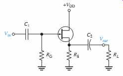
FIG. 18 JFET common-drain amplifier (source-follower).
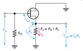
FIG. 19 Voltages in a common-drain amplifier with a load resistor
shown combined with RS.
Voltage Gain
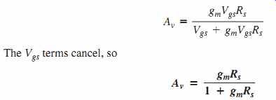
As in all amplifiers, the voltage gain is Av = Vout/Vin. For the source-follower, Vout is IdRs and Vin is Vgs + IdRs, as shown in FIG. 19. Therefore, the gate-to-source voltage gain is IdRs (Vgs + IdRs). Substituting Id=gm Vgs into the expression gives the following result:
Equation 6
The Vgs terms cancel, so Notice here that the gain is always slightly less than 1. If then a good approximation is Since the output voltage is at the source, it is in phase with the gate (input) voltage.
Input Resistance
Because the input signal is applied to the gate, the input resistance seen by the input sig nal source is extremely high, just as in the common-source amplifier configuration. The gate resistor, RG, in parallel with the input resistance looking in at the gate is the total input resistance.
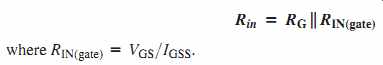
Equation 7
Section 2 CHECKUP
1. What is the ideal maximum voltage gain of a common-drain amplifier?
2. What factors influence the voltage gain of a common-drain amplifier?
3. THE COMMON-GATE AMPLIFIER
The common-gate FET amplifier configuration is comparable to the common-base BJT amplifier. Like the CB, the common-gate (CG) amplifier has a low input resistance. This is different from the CS and CD configurations, which have very high input resistances.
After completing this section, you should be able to:
- Explain and analyze the operation of common-gate FET amplifiers
- Analyze common-gate JFET amplifier operation
- Determine the voltage gain
- Determine the input resistance
- Describe and analyze the cascode amplifier
- Determine the voltage gain
- Determine the input resistance
Common-Gate Amplifier Operation
A self-biased common-gate amplifier is shown in FIG. 22. The gate is connected directly to ground. The input signal is applied at the source terminal through C1. The output is coupled through C2 from the drain terminal.
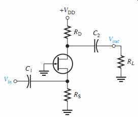
FIG. 22 JFET common-gate amplifier.
Voltage Gain--The voltage gain from source to drain is developed as follows:
Equation 8
where Rd = RD || RL. Notice that the gain expression is the same as for the common-source JFET amplifier.
Input Resistance---As you have seen, both the common-source and common-drain configurations have extremely high input resistances because the gate is the input terminal. In contrast, the common-gate configuration where the source is the input terminal has a low input resistance. This is shown as follows. First, the input current is equal to the drain current.
Equation 9
If, for example, gm has a value of then 4000 mS,
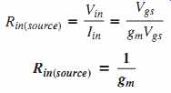
Rin(source) = 1/ 4000 mS = 250 OHM
The Cascode Amplifier
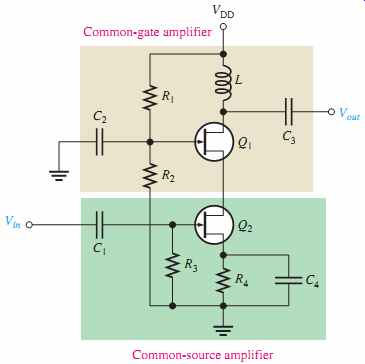
FIG. 24 A JFET cascode amplifier.
One application in which the common-gate configuration is found is the cascode amplifier, commonly used for RF (radio frequency) applications. A cascode amplifier is one in which a common-source amplifier and a common-gate amplifier are connected in a series arrangement.
BJTs can also be used to form cascode amplifiers (a common-emitter and a common-base). A JFET cascode amplifier circuit is shown in FIG. 24. The input stage is a common-source amplifier, and its load is a common-gate amplifier connected in the drain circuit.
The cascode amplifier using JFETs provides a very high input resistance and significantly reduces capacitive effects to allow for operation at much higher frequencies than a common-source amplifier alone. Internal capacitances, which exist in every type of transistor, become significant at higher frequencies and reduce the gain of inverting amplifiers as described by the Miller effect, covered in section 10. The first stage is a CS amplifier that inverts the signal. However, the gain is very low because of the low input resistance of the CB amplifier that it is driving. As a result, the effect of internal capacitances on the high-frequency response is very small. The second stage is a CG amplifier that does not invert the signal, so it can have high gain without degrading the high-frequency response.
The combination of the two amplifiers provides the best of both circuits, resulting in high gain, high input resistance, and an excellent high-frequency response.
The voltage gain of the cascode amplifier in FIG. 24 is a product of the gains of both the CS and the CG stages. However, as mentioned, the gain is primarily provided by the CG amplifier.
Av = agm(CS) a 1 gm(CG) bb(gm(CG)XL) _ gm(CG) XL
Since Rd of the CS amplifier stage is the input resistance of the CG stage and XL is the reactance of the inductor in the drain of the CG stage, the voltage gain is…
Av = Av(CS) Av(CG) = (gm(CS)Rd)(gm(CG)XL)
… assuming the trans-conductances of both transistors are approximately the same. From the equation you can see that the voltage gain increases with frequency because XL increases.
As the frequency continues to increase, eventually capacitance effects become significant enough to begin reducing the gain.
The input resistance to the cascade amplifier is the input resistance to the CS stage.
Rin = R3 || [VGS /IGSS ]
Section 3 CHECKUP
1. What is a major difference between a common-gate amplifier and the other two con figurations?
2. What common factor determines the voltage gain and the input resistance of a common-gate amplifier?
3. Name the advantages of a cascode amplifier.
4. THE CLASS D AMPLIFIER
In section 7, class A, class B, and class AB amplifiers were introduced. Those types of amplifiers are generally implemented with either BJTs or FETs. The class D amplifier, however, primarily uses only MOSFETs. The class D differs fundamentally from the other classes because its output transistors are switched on and off in response to an analog input instead of operating linearly over a continuous range of input values.
After completing this section, you should be able to:
- Discuss the operation of a class D amplifier
- Explain pulse-width modulation (PWM)
- Describe a basic pulse-width modulator
- Discuss frequency spectra
- Describe the complementary MOSFET stage
- Determine the efficiency
- Describe the purpose of the low-pass filter
- Describe the signal flow through a class D amplifier
In a class D amplifier, the output transistors are operated as switches instead of operating linearly as in the classes A, B, and AB. An advantage in audio applications is that a class D amplifier can operate at a maximum theoretical efficiency of 100% compared to class A at 25% and class B/AB at 79%. In practice, efficiencies over 90% can be achieved with class D.
A basic block diagram of a class D amplifier driving a speaker is shown in FIG. 25.
It consists of a pulse-width modulator driving complementary MOSFET output transistors operating as switches and followed by a low-pass filter. Most class D amplifiers operate on dual-polarity power supplies. The MOSFETs are basically push-pull amplifiers that are operated as switching devices, rather than linear devices as in the case of class B amplifiers.
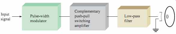
FIG. 25 Basic class D audio amplifier.
Pulse-Width Modulation (PWM)
FIG. 26 Pulse-width modulated sine wave.
Pulse-width modulation is a process in which an input signal is converted to a series of pulses with widths that vary proportionally to the amplitude of the input signal. This is illustrated in FIG. 26 for one cycle of a sinusoidal signal. Notice that the pulse width is wider when the amplitude is positive and narrower when the amplitude is negative. The output will be a square wave if the input is zero.
The PWM signal is typically produced using a comparator circuit. Comparators are discussed in more detail in section 13, but here is a basic explanation of how they work. A comparator has two inputs and one output, as shown by the symbol in FIG. 27. The input labeled + is called the noninverting input, and the input labeled _ is the inverting input. When the voltage on the inverting input exceeds the voltage on the noninverting input, the comparator switches to its negative saturated output state. When the voltage on the noninverting input exceeds the voltage on the inverting input, the comparator switches to its positive saturated output state. This is illustrated in FIG. 27 for one cycle of a sine wave voltage on the non inverting input and a higher frequency triangular wave voltage on the inverting input.
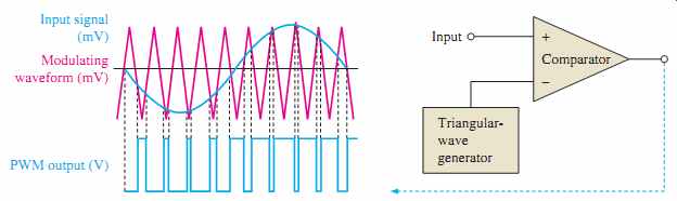
FIG. 27 A basic pulse-width modulator.
The comparator inputs are typically very small voltages (mV range); and the comparator output is "rail-to-rail," which means that the positive maximum is near the positive dc supply voltage and the negative maximum is near the negative dc supply voltage. An output of 12 V or 24 V peak-to-peak is not unusual. From this, you can see that the gain can be quite high. For example, if the input signal is 10 mVpp, the voltage gain is 24 Vpp/ 10 mVpp = 2400. Since the comparator output amplitude is constant for a specified range of input voltages, the gain is dependent on the input signal voltage. If the input signal is 100 mVpp, the output is still 24 Vpp, and the gain is 240 instead of 2400.
Frequency Spectra---All nonsinusoidal waveforms are made up of harmonic frequencies.
The frequency content of a particular waveform is called its spectrum. When the triangular waveform modulates the input sine wave, the resulting spectrum contains the sine wave frequency, finput, plus the fundamental frequency of the triangular modulating signal, fm, and harmonic frequencies above and below the fundamental frequency. These harmonic frequencies are due to the fast rise and fall times of the PWM signal and the flat areas between the pulses.
A simplified frequency spectrum of a PWM signal is shown in FIG. 28. The frequency of the triangular waveform must be significantly higher than the highest input signal frequency so that the lowest frequency harmonic is well above the range of input signal frequencies.
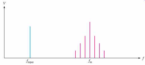
FIG. 28 Frequency spectrum of a PWM signal.
The Complementary MOSFET Stage
The MOSFETs are arranged in a common-source complementary configuration to provide power gain. Each transistor switches between the on state and the off state and when one transistor is on, the other one is off, as shown in FIG. 29. When a transistor is on, there is very little voltage across it and, therefore, there is very little power dissipated even though it may have a high current through it. When a transistor is off, there is no current through it and, therefore, there is no power dissipated. The only time power is dissipated in the transistors is during the short switching time. Power delivered to a load can be very high because a load will have a voltage across it nearly equal to the supply voltages and a high current through it.
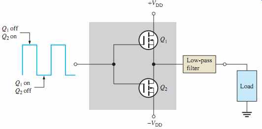
FIG. 29 Complementary MOSFETs operating as switches to amplify power.
Efficiency
When Q1 is on, it is providing current to the load. However, ideally the volt age across it is zero so the internal power dissipated by Q1 is:
At the same time, Q2 is off and the current through it is zero, so the internal power is:
Ideally, the output power to the load is 2VQ IL. The maximum ideal efficiency is, therefore,
As a percentage, eta_max = 100%.
In a practical case, each MOSFET would have a few tenths of a volt across it in the on state. There is also a small internal power dissipation in the comparator and triangular wave generator. Also, power is dissipated during the finite switching time, so the ideal efficiency of 100% can never be reached in practice.
Low-Pass Filter
The low-pass filter removes the modulating frequency and harmonics and passes only the original signal to the output. The filter has a bandwidth that passes only the input signal frequencies, as illustrated in FIG. 30.
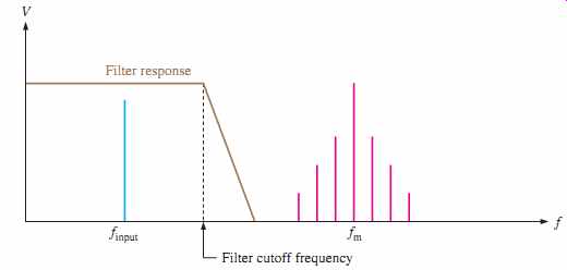
FIG. 30 The low-pass filter removes all but the input signal frequency
from the PWM signal.
Signal Flow
FIG. 31 shows the signals at each point in a class D amplifier. A small audio signal is applied and pulse-width modulated to produce a PWM signal at the output of the modulator where voltage gain is achieved. The PWM drives the complementary MOSFET stage to achieve power amplification. The PWM signal is filtered and the amplified audio signal appears on the output with sufficient power to drive a speaker.
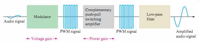
FIG. 31 Signal flow in a class D amplifier.
Section 4 CHECKUP
1. Name the three stages of a class D amplifier.
2. In pulse-width modulation, to what is the pulse width proportional?
3. How is the PWM signal changed to an audio signal?
5. MOSFET ANALOG SWITCHING
MOSFETs are widely used in analog and digital switching applications. In the preceding section, you saw how MOSFETs are used in the switching mode in Class D amplifiers.
Generally, they exhibit very low on-resistance, very high off-resistance, and fast switching times.
After completing this section, you should be able to:
- Describe how MOSFETs can be used in analog switching applications
- Explain how a MOSFET operates as a switch
- Discuss load line operation
---Discuss the ideal switch
- Describe a MOSFET analog switch
- Discuss analog switch applications
- Explain a sampling circuit
---Explain an analog multiplexer
---Explain a switched-capacitor circuit
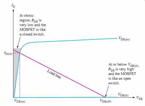
FIG. 32 Switching operation on the load line.
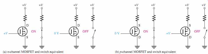
FIG. 33 The MOSFET as a switch.
MOSFET Switching Operation
E-MOSFETs are generally used for switching applications because of their threshold characteristic, VGS(th). When the gate-to-source voltage is less than the threshold value, the MOSFET is off. When the gate-to-source voltage is greater than the threshold value, the MOSFET is on. When VGS is varied between VGS(th) and VGS(on), the MOSFET is being operated as a switch, as illustrated in FIG. 32. In the off state, when the device is operating at the lower end of the load line and acts like an open switch (very high RDS). When VGS is sufficiently greater than VGS(th), the device is operating at the upper end of the load line in the ohmic region and acts like a closed switch (very low RDS).
The Ideal Switch---Refer to FIG. 33(a). When the gate voltage of the n-channel MOSFET is _V, the gate is more positive than the source by an amount exceeding VGS(th).
The MOSFET is on and appears as a closed switch between the drain and source. When the gate voltage is zero, the gate-to-source voltage is 0V. The MOSFET is off and appears as an open switch between the drain and source.
Refer to FIG. 33(b). When the gate voltage of the p-channel MOSFET is 0 V, the gate is less positive than the source by an amount exceeding VGS(th). The MOSFET is on and appears as a closed switch between the drain and source. When the gate voltage is _V, the gate-to-source voltage is 0 V. The MOSFET is off and appears as an open switch between the drain and source.
VGS 6 VGS(th),
The Analog Switch---MOSFETs are commonly used for switching analog signals. Basically, a signal applied to the drain can be switched through to the source by a voltage on the gate. A major restriction is that the signal level at the source must not cause the gate-to-source voltage to drop below VGS(th).
A basic n-channel MOSFET analog switch is shown in FIG. 34. The signal at the drain is connected to the source when the MOSFET is turned on by a positive VGS and is disconnected when VGS is 0, as indicated.
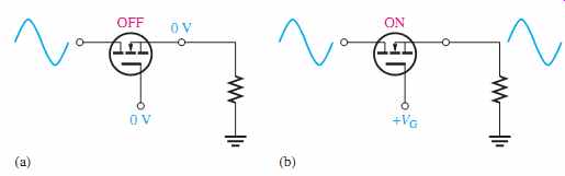
FIG. 34 Operation of an n-channel MOSFET analog switch.
When the analog switch is on, as illustrated in FIG. 35, the minimum gate-to source voltage occurs at the negative peak of the signal. The difference in VG and -Vp(out) is the gate-to-source voltage at the instant of the negative peak and must be equal to or greater than VGS(th) to keep the MOSFET in conduction.
VGS = VG - Vp(out) Ú VGS(th)
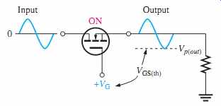
FIG. 35 Signal amplitude is limited by VGS(th).
Analog Switch Applications
Sampling Circuit---One application of analog switches is in analog-to-digital conversion.
The analog switch is used in a sample-and-hold circuit to sample the input signal at a certain rate. Each sampled signal value is then temporarily stored on a capacitor until it can be converted to a digital code by an analog-to-digital converter (ADC). To accomplish this, the MOSFET is turned on for short intervals during one cycle of the input signal by pulses applied to the gate. The basic operation, showing only a few samples for clarity, is illustrated in FIG. 36.
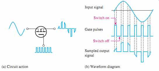
FIG. 36 The analog switch operating as a sampling circuit.
The minimum rate at which a signal can be sampled and reconstructed from the samples must be more than twice the maximum frequency contained in the signal. The minimum sampling frequency is called the Nyquist frequency.
fsample (min) > 2fsignal (max)
When a gate pulse is at its high level, the switch is turned on and the small portion of the input waveform occurring during that pulse appears on the output. When the pulse wave form is at its 0 V level, the switch is turned off and the output is also at 0 V.
Analog Multiplexer
Analog multiplexers are used where two or more signals are to be routed to the same destination. For example, a two-channel analog sampling multiplexer is shown in FIG. 37. The MOSFETs are alternately turned on and off so that first one signal sample is connected to the output and then the other. The pulses are applied to the gate of switch A, and the inverted pulses are applied to the gate of switch B. A digital circuit known as an inverter is used for this. When the pulses are high, switch A is on and switch B is off. When the pulses are low, switch B is on and switch A is off. This is called time division multiplexing because signal A appears on the output during time intervals when the pulse is high and signal B appears during the time intervals when the pulse is low. That is, they are interleaved on a time basis for transmission on a single line.
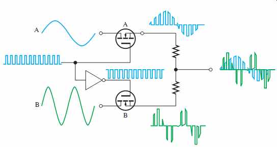
FIG. 37 The analog multiplexer is alternately sampling two signals
and interleaving them on a single output line.
Switched-Capacitor Circuit
Another application of MOSFETs is in switched-capacitor circuits commonly used in integrated circuit programmable analog devices known as analog signal processors. Because capacitors can be implemented in ICs more easily than a resistor, they are used to emulate resistors. Capacitors also take up less space on a chip than an IC resistor and dissipate no power. Many types of analog circuits use resistors to determine voltage gain and other characteristics and by using switched capacitors to emu late resistors, dynamic programming of analog circuits can be achieved.
For example, in a certain type of IC amplifier circuit that you will study later, two external resistors are required as shown in FIG. 38. The values of these resistors establish the voltage gain of the amplifier as Av= R2/R1.
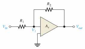
FIG. 38 A type of IC amplifier.
A switched-capacitor can be used to emulate a resistor as shown in FIG. 39 using a mechanical switch analogy (MOSFETs are actually used as the switches). Switch 1 and switch 2 are alternately turned on and off at a certain frequency to charge or discharge C, depending on the values of the voltage sources. In the case of R1 in FIG. 38, Vin and V1 are represented by VA and VB, respectively. For R2, V1 and Vout are represented by VA and VB, respectively.
It can be shown that the capacitor emulates a resistance with a value that depends on the frequency at which the switches are turned on and off and the capacitance value.
R = 1/fC

Equation 10
By changing the frequency, the effective resistance value can be altered.
Complementary E-MOSFETs and capacitors can be used to replace the resistors in the amplifier, as shown in FIG. 40. When Q1 is on, Q2 is off and vice versa. The frequency f1 and C1 are selected to provide the required value of R1. Likewise, f2 and C2 provide the required value of R2. To reprogram the amplifier for a different gain, the frequencies are changed.
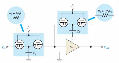
FIG. 40 The IC amplifier in FIG. 38 with switched-capacitor circuits
replacing the resistors.
Section 5 CHECKUP
1. When does an E-MOSFET act as an open switch?
2. When does an E-MOSFET act as a closed switch?
3. What type of voltage is generally used to control an analog switch?
4. In a switched-capacitor circuit, on what does the emulated resistance depend?