AMAZON multi-meters discounts AMAZON oscilloscope discounts
<< cont. from part 1
6. MOSFET DIGITAL SWITCHING
In the preceding section, you saw how MOSFETs are used to switch analog signals.
MOSFETs are also used in switching applications in digital integrated circuits and in power control circuits. MOSFETs used in digital ICs are low-power types, and those used in power control are high-power devices.
Goals:
- Describe how MOSFETs are used in digital switching applications
- Discuss complementary MOS (CMOS)
- Explain CMOS inverter operation
-Explain CMOS NAND gate operation
- Explain CMOS NOR gate operation
- Discuss MOSFETs in power switching
CMOS (Complementary MOS)
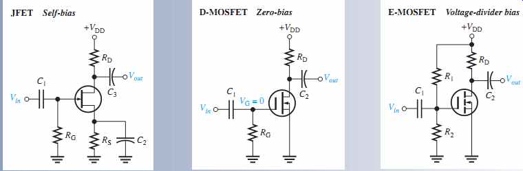
CMOS combines n-channel and p-channel E-MOSFETs in a series arrangement as shown in FIG. 41(a). The input voltage at the gates is either 0 V or VDD. Notice that VDD and ground are both connected to source terminals of the transistors. To avoid confusion, the term VDD is used for the positive voltage, which is on the p-channel device's source terminal.
When Vin = 0 V, Q1 is on and Q2 is off, as shown in part (b). Because Q1 is acting as a closed switch, the output is approximately VDD. When Vin = VDD, Q2 is on and Q1 is off, as shown in part (c). Because Q2 is acting as a closed switch, the output is essentially connected to ground (0 V).
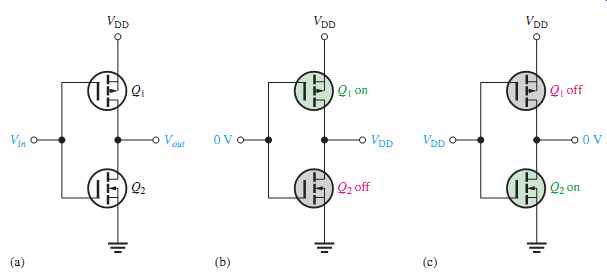
FIG. 41 CMOS inverter operation.
A major advantage of CMOS is that it consumes very little dc power. Because the MOSFETs are in series and one of them is always off, there is essentially no current from the dc supply in the quiescent state. When the MOSFETs are switching, there is current for a very short time because both transistors are on during this very short transition from one state to the other.
Inverter---Notice that the circuit in FIG. 41 actually inverts the input because when the input is 0 V or low, the output is VDD or high. When the input is VDD or high, the out put is 0 V or low. For this reason, this circuit is called an inverter in digital electronics.
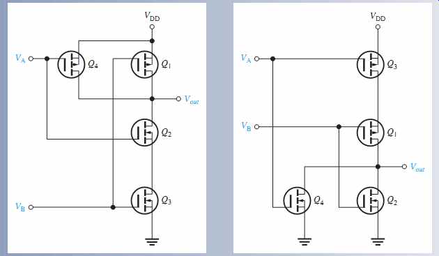
NAND Gate--- In FIG. 42(a), two additional MOSFETs and a second input are added to the CMOS pair to create a digital circuit known as a NAND gate. Q4 is connected in parallel with Q1, and Q3 is connected in series with Q2. When both inputs, VA and VB, are 0, Q1 and Q4 are on while Q2 and Q3 are off, making Vout VDD. When both inputs are equal to VDD, Q1 and Q4 are off while Q2 and Q3 are on, making Vout 0. You can verify that when the inputs are different, one at VDD and the other at 0, the output is equal to VDD. The operation is summarized in the table of FIG. 42(b) and can be stated:
When VA AND VB are high, the output is low; otherwise, the output is high.
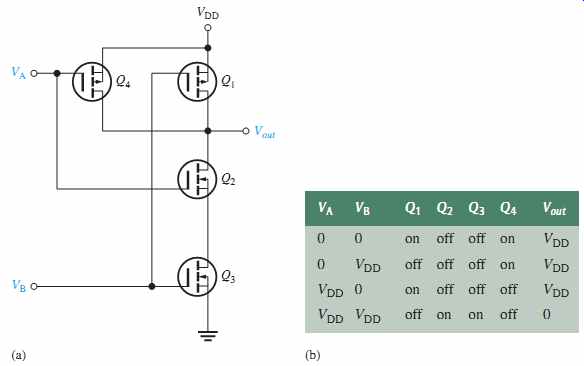
FIG. 42 CMOS NAND gate operation.
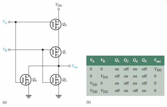
FIG. 43 CMOS NOR gate operation.
NOR Gate ---In FIG. 43(a), two additional MOSFETs and a second input are added to the CMOS pair to create a digital circuit known as a NOR gate. Q4 is connected in parallel with Q2, and Q3 is connected in series with Q1. When both inputs, VA and VB, are 0, Q1 and Q3 are on while Q2 and Q4 are off, making Vout VDD. When both inputs are equal to VDD, Q1 and Q3 are off while Q2 and Q4 are on, making Vout 0. You can verify that when the inputs are different, one at VDD and the other at 0, the output is equal to 0. The operation is summarized in the table of FIG. 43(b) and can be stated:
When VA OR VB OR both are high, the output is low; otherwise, the output is high.
MOSFETs in Power Switching
The BJT was the only power transistor until the MOSFET was introduced. The BJT requires a base current to turn on, has relatively slow turn-off characteristics, and is susceptible to thermal runaway due to a negative temperature coefficient. The MOSFET, how ever, is voltage controlled and has a positive temperature coefficient, which prevents thermal runaway. The MOSFET can turn off faster than the BJT, and the low on-state-resistance results in conduction power losses lower than with BJTs. Power MOSFETs are used for motor control, dc-to-ac conversion, dc-to-dc conversion, load switching, and other applications that require high current and precise digital control.
Section 6 CHECKUP
1. Describe a basic CMOS inverter.
2. What type of 2-input digital CMOS circuit has a low output only when both inputs are high?
3. What type of 2-input digital CMOS circuit has a high output only when both inputs are low?
7. TROUBLESHOOTING
A technician who understands the basics of circuit operation and who can, if necessary, perform basic analysis on a given circuit is much more valuable than one who is limited to carrying out routine test procedures. In this section, you will see how to test a circuit board that has only a schematic with no specified test procedure or voltage levels. In this case, basic knowledge of how the circuit operates and the ability to do a quick circuit analysis are useful.
After completing this section, you should be able to:
- Troubleshoot FET amplifiers
- Troubleshoot a two-stage common-source amplifier
- Explain each step in the troubleshooting procedure
---Use a datasheet
- Relate the circuit board to the schematic
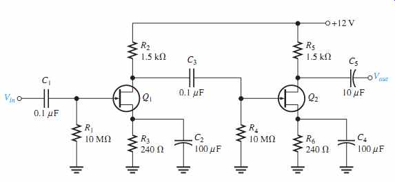
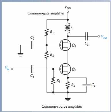
FIG. 46 A two-stage CS JFET amplifier circuit.
A Two-Stage Common-Source Amplifier
Assume that you are given a circuit board containing an audio amplifier and told simply that it is not working properly. The circuit is a two-stage CS JFET amplifier, as shown in FIG. 46.
The problem is approached in the following sequence.
Step 1: Determine what the voltage levels in the circuit should be so that you know what to look for. First, pull a datasheet on the particular transistor (assume both Q1 and Q2 are found to be the same type of transistor) and determine the gm so that you can calculate the typical voltage gain. Assume that for this particular device, a typical gm of is specified. Calculate the expected typical voltage gain of each stage (notice they are identical) based on the typical value of gm. The gm of actual devices may be any value between the specified minimum and maximum values. Because the input resistance is very high, the second stage does not significantly load the first stage, as in a BJT amplifier. So, the unloaded voltage gain for each stage is Since the stages are identical, the typical overall gain should be Assume the dc levels have been checked and verified. You are now ready to move to ac signal checks.
Step 2: Arrange a test setup to permit connection of an input test signal, a dc supply voltage, and ground to the circuit. The schematic shows that the dc supply voltage must be +12 V. Choose 10 mV rms as an input test signal. This value is arbitrary (although the capability of your signal source is a factor), but small enough that the expected output signal voltage is well below the absolute peak-to-peak limit of 12 V set by the supply voltage and ground (you know that the output voltage swing cannot go higher than 12 V or lower than 0 V). Set the frequency of the sinusoidal signal source to an arbitrary value in the audio range (say 10 kHz) because you know this is an audio amplifier. The audio frequency range is generally accepted as 20 Hz to 20 kHz.
Step 3: Check the input signal at the gate of Q1 and the output signal at the drain of Q2 with an oscilloscope. The results are shown in FIG. 47. The measured output voltage has a peak value of 226 mV. The expected typical peak output voltage is:
The output is much less than it should be.
Step 4: Trace the signal from the output toward the input to determine the fault.
FIG. 47 shows the oscilloscope displays of the measured signal voltages. The voltage at the gate of Q2 is 106 mV peak, as expected This signal is properly coupled from the drain of Q1. Therefore, the problem lies in the second stage. From the oscilloscope displays, the gain of Q2 is much lower than it should be (213 mV 100 mV = 2.13 instead of 7.5).
Step 5: Analyze the possible causes of the observed malfunction. There are three possible reasons the gain is low:
1. Q2 has a lower transconductance (gm) than the specified typical value.
Check the datasheet to see if the minimum gm accounts for the lower measured gain.
2. R5 has a lower value than shown on the schematic. An incorrect value should show up with dc voltage checks, particularly if the value is much different than specified, so this is not the likely cause in this case.
3. The bypass capacitor C4 is open.
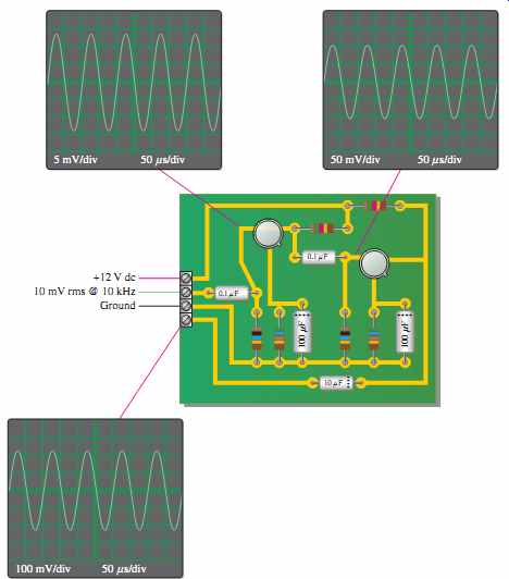
FIG. 47 Oscilloscope displays of signals in the two-stage JFET amplifier.
The best way to check the gm is by replacing Q2 with a new transistor of the same type and rechecking the output signal. You can make certain that R5 is the proper value by removing one end of the resistor from the circuit board and measuring the resistance with an ohmmeter. To avoid having to unsolder a component, the best way to start isolating the fault is by checking the signal voltage at the source of Q2. If the capacitor is working properly, there will be only a dc voltage at the source. The presence of a signal voltage at the source indicates that C4 is open. With R6 unbypassed, the gain expression is rather than simply gmRd, thus resulting in less gain. gmRd>(1 + gmRs)
Section 7 CHECKUP
1. What is the prerequisite to effective troubleshooting?
2. Assume that C2 in the amplifier of FIG. 46 opened. What symptoms would indicate this failure?
3. If C3 opened in the amplifier of FIG. 46, would the voltage gain of the first stage be affected?
=========
Application Activity: Active Antenna
In this application, a broadband JFET amplifier is used to provide a high input impedance and voltage gain for a whip antenna. When an antenna is connected to the input of a receiver or a coaxial cable, signal deterioration may be unacceptable due to a distant station, noisy conditions, or an impedance mismatch. An active antenna can alleviate this problem by providing a stronger signal. The block diagram in FIG. 48 shows an active antenna, followed by a low impedance output buffer to drive a coaxial cable or a receiver input. The focus in this application is the active antenna. The low output impedance buffer can be a BJT emitter-follower or an impedance-matching transformer.
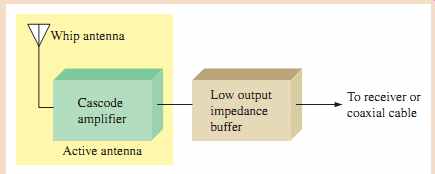
FIG. 48 An active antenna driving a receiver or a coax through a buffer.
The Amplifier Circuit FIG. 49 is a broadband amplifier using two JFETs in a cascode arrangement commonly used in RF (radio frequency) applications. The advantage of using a JFET is that its high input impedance does not load the antenna and cause a reduction in signal volt age, resulting in poor signal reception. It also is a low noise device and can be located close to the antenna before additional noise is picked up by the system. Generally, an antenna produces signal voltages in the microvolt range, and any signal loss because of loading or noise can significantly degrade the signal. The active antenna also provides a large voltage gain that results in a stronger signal to the receiver with improved signal-to noise ratio. The active antenna is powered by a separate 9 V battery, which also provides isolation from noise pickup in the signal lines and is located in an enclosed metal box to provide additional isolation.
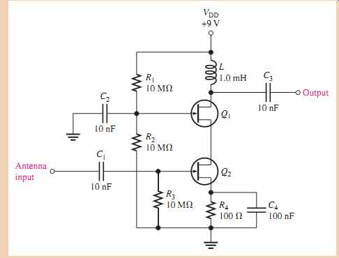
FIG. 49 Cascode amplifier for active antenna.
This active antenna has a voltage gain of approximately 2000 at 88 MHz and a gain of approximately 10,000 at 1 GHz which makes it applicable for the FM broadcast band, some TV channel bands, some amateur radio (HAM) bands, cell phone bands, and many others. Also below the FM band, the gain may be adequate for other radio and TV bands as well, depending on receiver requirements. The coil can be changed to optimize gain within a specified band or to adjust the band downward.
1. Research the Internet to determine the frequency band for TV channels 7-13.
2. Research the Internet to find the frequency bands allocated for cellular telephones.
3. What is the purpose of C2 in FIG. 49? The transistors used in the active antenna are 2N5484 n-channel JFETs. The partial datasheet is shown in FIG. 50.
4. Using the datasheet, determine RIN(gate) of the JFET (Q2).
5. What input resistance is presented to the antenna in FIG. 49?
6. From the datasheet, what is the minimum forward transconductance? Simulation
The active antenna circuit is simulated in Multisim with the antenna input represented by a peak source. The output signal is shown for 88 MHz and 1 GHz inputs in FIG. 51.
7. What is the significance of the 88 MHz frequency?
8. Determine the rms output voltage in FIG. 51(b) and (c), and calculate the gain for both frequencies.
Simulate the active antenna circuit using your Multisim software. Measure the output voltage at 10 MHz, 100 MHz, and 500 MHz.
Prototyping and Testing
Now that the circuit has been simulated, the prototype circuit is constructed and tested.
After the circuit is successfully tested, it is ready to be finalized. Because you are working at high frequencies where stray capacitances can cause unwanted resonant conditions, the circuit layout is very critical.
10 mV

FIG. 50 Partial datasheet for the 2N5484 RF n-channel JFET. Copyright
Fairchild semiconductor corporation.
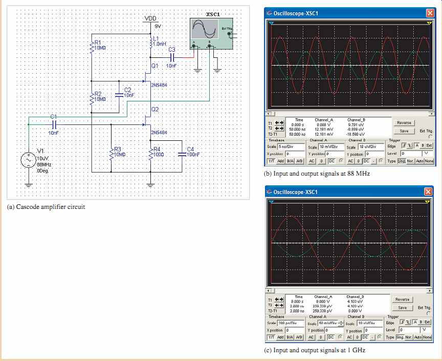
FIG. 51 Simulation results for the active antenna circuit. Input is
green and output is red.
Certain considerations should be observed when laying out a printed circuit board for RF circuits. EMI (electromagnetic interference), line inductance, and stray capacitance all become important at high frequencies. A few basic features that should be incorporated on an RF circuit board are
- Keep traces as short and wide as possible.
- Do not run parallel signal lines that are in close proximity.
- Capacitively decouple supply voltages.
- Provide a large ground plane for shielding and to minimize noise.
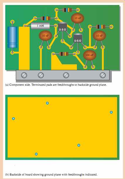
FIG. 52 Active antenna circuit board.
The circuit board for the active antenna is shown in FIG. 52. A large ground plane is on the back side. Components are connected to the ground plane with feedthrough connections as indicated.
9. Check the printed circuit board for correctness by comparing with the schematic in FIG. 49.
10. State the purpose of the large blue capacitor that is not shown on the schematic.
11. Label each input and output pin according to function.
The Complete Active Antenna Unit
Typically, the active antenna circuit should be enclosed in a metal box for proper shielding, similar to that shown in FIG. 53. The particular configuration shown includes an impedance-matching transformer connected to a type of connector (BNC) used with coaxial cables for illustration. Other interface configurations, such as an emitter-follower output may be used for interfacing. The particular antenna shown is a telescoping whip antenna.
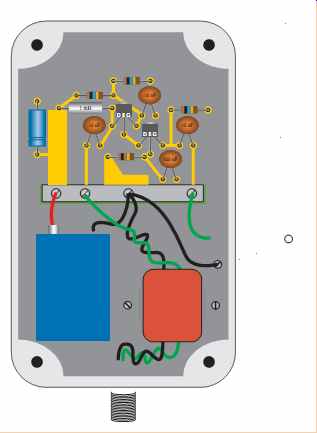
FIG. 53 A configuration of the active antenna in a metal housing (cover
removed) with a 9 V battery and an impedance matching transformer.
==========
==========
SUMMARY OF FET AMPLIFIERS
COMMON-SOURCE AMPLIFIERS

===========
SUMMARY
Section 1
- The transconductance, gm, of a FET relates the output current, Id, to the input voltage, Vgs.
- The voltage gain of a common-source amplifier is determined largely by the transconductance, gm, and the drain resistance, Rd.
- The internal drain-to-source resistance, r’ ds, of a FET influences (reduces) the gain if it is not sufficiently greater than Rd so that it can be neglected.
- An unbypassed resistance between source and ground (RS) reduces the voltage gain of a FET amplifier.
- A load resistance connected to the drain of a common-source amplifier reduces the voltage gain.
- There is a 180° phase inversion between gate and drain voltages.
- The input resistance at the gate of a FET is extremely high.
Section 2
- The voltage gain of a common-drain amplifier (source-follower) is always slightly less than 1.
- There is no phase inversion between gate and source in a source-follower.
Section 3
- The input resistance of a common-gate amplifier is the reciprocal of gm.
- The cascode amplifier combines a CS amplifier and a CG amplifier.
Section 4
- The class D amplifier is a nonlinear amplifier because the transistors operate as switches.
- The class D amplifier uses pulse-width modulation (PWM) to represent the input signal.
- A low-pass filter converts the PWM signal back to the original input signal.
- The efficiency of a class D amplifier approaches 100%.
Section 5
- An analog switch passes or blocks an analog signal when turned on or off by a digital control input.
- A sampling circuit is an analog switch that is turned on for short time intervals to allow a sufficient number of discrete input signal values to appear on the output so that the input signal can be accurately represented by those discrete values.
- An analog multiplexer consists of two or more analog switches that connect sampled portions of their analog input signals to a single output in a time sequence.
- Switched-capacitors are used to emulate resistance in programmable IC analog arrays.
Section 6
- Complementary MOS (CMOS) is used in low-power digital switching circuits.
- CMOS uses an n-channel MOSFET and a p-channel MOSFET connected in series.
- The inverter, NAND gate, and NOR gate are examples of digital logic circuits.
TERMS
Key terms and other bold terms in the section are defined in the end-of-book glossary.
Analog switch --A device that switches an analog signal on and off.
Class D --A nonlinear amplifier in which the transistors are operated as switches.
CMOS-- Complementary MOS.
Common-drain --A FET amplifier configuration in which the drain is the grounded terminal.
Common-gate --A FET amplifier configuration in which the gate is the grounded terminal.
Common-source --A FET amplifier configuration in which the source is the grounded terminal.
Pulse-width modulation --A process in which a signal is converted to a series of pulses with widths that vary proportionally to the signal amplitude.
Source-follower --The common-drain amplifier.
FORMULAS [coming soon]
TRUE/FALSE QUIZ
1. A common-source (CS) amplifier has a very high input resistance.
2. The drain current in a CS amplifier can be calculated using a quadratic formula.
3. The voltage gain of a CS amplifier is the transconductance times the source resistance.
4. There is no phase inversion in a CS amplifier.
5. A CS amplifier using a D-MOSFET can operate with both positive and negative input voltages.
6. A common-drain (CD) amplifier is called a drain-follower.
7. The input resistance of a CD amplifier is very low.
8. The input resistance of a common-gate (CG) amplifier is very low.
9. A cascode amplifier uses both a CS and a CG amplifier.
10. The class D amplifier always operates in the linear region.
11. The class D amplifier uses pulse-width modulation.
12. An analog switch is controlled by a digital input.
13. The purpose of a switched-capacitor circuit is to emulate resistance.
14. CMOS is a device used in linear amplifiers.
15. CMOS utilizes a pnp MOSFET and an npn MOSFET connected together.
CIRCUIT QUIZ
1. If the drain current is increased in FIG. 9, VGS will (a) increase (b) decrease (c) not change
2. If the JFET in FIG. 9 is substituted with one having a lower value of IDSS, the voltage gain will (a) increase (b) decrease (c) not change
3. If the JFET in FIG. 9 is substituted with one having a lower value of VGS(off ), the voltage gain will (a) increase (b) decrease (c) not change
4. If the value of RG in FIG. 9 is increased, VGS will (a) increase (b) decrease (c) not change
5. If the value of RG in FIG. 11 is increased, the input resistance seen by the signal source will (a) increase (b) decrease (c) not change
6. If the value of R1 in FIG. 17 is increased, VGS will (a) increase (b) decrease (c) not change
7. If the value of RL in FIG. 17 is decreased, the voltage gain will (a) increase (b) decrease (c) not change
8. If the value of RS in FIG. 20 is increased, the voltage gain will (a) increase (b) decrease (c) not change
9. If C4 in FIG. 46 opens, the output signal voltage will (a) increase (b) decrease (c) not change
SELF-TEST
Section 1
1. In a common-source amplifier, the output voltage is (a) out of phase with the input (b) in phase with the input (c) taken at the source (d) taken at the drain (e) answers (a) and (c) (f ) answers (a) and (d)
2. In a certain common-source (CS) amplifier, Vds = 3.2 V rms and Vgs = 280 mV rms. The voltage gain is (a) 1
(b) 11.4
(c) 8.75
(d) 3.2
3. In a certain CS amplifier, If the source resistor is completely bypassed, the voltage gain is:
(a) 450
(b) 45
(c) 4.5
(d) 2.52
4. Ideally, the equivalent circuit of a FET contains (a) a current source in series with a resistance (b) a resistance between drain and source terminals (c) a current source between gate and source terminals (d) a current source between drain and source terminals
5. The value of the current source in Question 4 is dependent on the (a) transconductance and gate-to-source voltage (b) dc supply voltage (c) external drain resistance (d) answers (b) and (c)
6. A certain common-source amplifier has a voltage gain of 10. If the source bypass capacitor is removed, (a) the voltage gain will increase (b) the transconductance will increase (c) the voltage gain will decrease (d) the Q-point will shift
7. A CS amplifier has a load resistance of:
If gm = 5 mS and 10 k OHM and RD = 820 OHM.
RD = 1.0 k OHM, RS = 560 OHM, VDD = 10 V, and gm = 4500 mS.
180° Vin= 500 mV, the output signal voltage is:
(a) 1.89 V
(b) 2.05 V
(c) 25 V (d) 0.5 V
8. If the load resistance in Question 7 is removed, the output voltage will (a) stay the same (b) decrease (c) increase (d) be zero
Section 2
9. A certain common-drain (CD) amplifier with has a transconductance of The voltage gain is (a) 1 (b) 0.86 (c) 0.98 (d) 6 6000 mS. RS = 1.0 kOHM
10. The datasheet for the transistor used in a CD amplifier specifies IGSS = 5 nA at VGS = 10 V. If the resistor from gate to ground, RG, is the total input resistance is approximately (a) (b) (c) (d) Section 3
11. The common-gate (CG) amplifier differs from both the CS and CD configurations in that it has a (a) much higher voltage gain (b) much lower voltage gain (c) much higher input resistance (d) much lower input resistance
12. If you are looking for both good voltage gain and high input resistance, you must use a (a) CS amplifier (b) CD amplifier (c) CG amplifier
13. A cascode amplifier consists of (a) a CD and a CS amplifier (b) a CS and a CG amplifier (c) a CG and a CD amplifier (d) two CG amplifiers
Section 4
14. The class D amplifier is similar to (a) class C (b) class B (c) class A (d) none of these
15. The class D amplifier uses (a) frequency modulation (b) amplitude modulation (c) pulse-width modulation (d) duty cycle modulation
Section 5
16. E-MOSFETs are generally used for switching applications because of their (a) threshold characteristic (b) high input resistance (c) linearity (d) high gain
17. A sampling circuit must sample a signal at a minimum of (a) one time per cycle (b) the signal frequency (c) twice the signal frequency (d) alternate cycles
18. The value of resistance emulated by a switched-capacitor circuit is a function of (a) voltage and capacitance (b) frequency and capacitance (c) gain and transconductance (d) frequency and transconductance
Section 6
19. A basic CMOS circuit uses a combination of (a) n-channel MOSFETs (b) p-channel MOSFETs (c) pnp and npn BJTs (d) an n-channel and a p-channel MOSFET 20. CMOS is commonly used in (a) digital circuits (b) linear circuits (c) RF circuits (d) power circuits
Section 7
21. If there is an internal open between the drain and source in a CS amplifier, the drain voltage is equal to (a) 0 V
(b) VDD
(c) VGS
(d) VGD
PROBLEMS
BASIC PROBLEMS
Section 1
The Common-Source Amplifier
1. A FET has a Determine the rms drain current for each of the following rms values of Vgs .
(a) 10 mV
(b) 150 mV
(c) 0.6 V
(d) 1 V
2. The gain of a certain JFET amplifier with a source resistance of zero is 20. Determine the drain resistance if the gm is
3. A certain FET amplifier has a gm of What is the volt age gain? Assume the source resistance is
4. What is the gain for the amplifier in Problem 3 if the source resistance is 1.0 k OHM?
0 OHM.
4.2 mS, r ‘ ds = 12 k OHM, and RD = 4.7 k OHM.
3500 mS.
gm = 6000 mS.
20.5 M OHM 40 M OHM 200 M OHM 50 M OHM 50 M OHM, +15 V -10 V +12 V
5. Identify the type of FET and its bias arrangement in FIG. 54. Ideally, what is VGS?
6. Calculate the dc voltages from each terminal to ground for the FETs in FIG. 54.
7. Identify each characteristic curve in FIG. 55 by the type of FET that it represents.
I I I
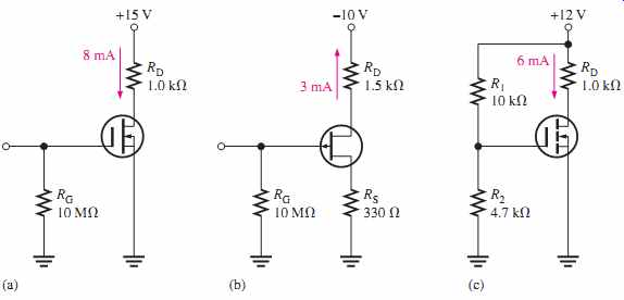
FIG. 54
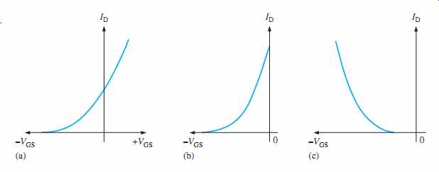
FIG. 55
8. Refer to the JFET transfer characteristic curve in FIG. 16(a) and determine the peak-to peak value of Id when Vgs is varied about its Q-point value.
9. Repeat Problem 8 for the curves in FIG. 16(b) and FIG. 16(c).
10. Given that ID = 2.83 mA in FIG. 56, find VDS and VGS. And
11. If a 50 mV rms input signal is applied to the amplifier in FIG. 56, what is the peak-to-peak output voltage?
12. If a load is ac coupled to the output in FIG. 56, what is the resulting output voltage (rms) when a 50 mV rms input is applied? gm = 5000 mS.
1500 OHM gm = 5000 mS.
IDSS = 8 mA. VGS(off) =-7 V
;1.5 V
FIG. 56
Multisim file circuits are identified with a logo and are in the Problems folder on the companion website.
Filenames correspond to figure numbers (e.g., F09-56).
13. Determine the voltage gain of each common-source amplifier in FIG. 57.
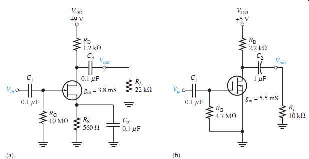
FIG. 57
14. Draw the dc and ac equivalent circuits for the amplifier in FIG. 58.
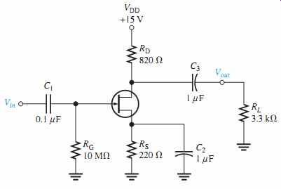
FIG. 58
15. Determine the drain current in FIG. 58 given that The Q-point is centered.
16. What is the gain of the amplifier in FIG. 58 if C2 is removed?
17. A resistor is connected in parallel with RL in FIG. 58. What is the voltage gain?
18. For the common-source amplifier in FIG. 59, determine ID, VGS, and VDS for a centered Q-point. IDSS = 9 mA, and VGS(off ) =-3 V.
4.7 k OHM IDSS = 15 mA and VGS(off ) =-4 V.
FIG. 59
19. If a 10 mV rms signal is applied to the input of the amplifier in FIG. 59, what is the rms value of the output signal?
20. Determine VGS, ID, and VDS for the amplifier in FIG. 60. ID(on) = 18 mA at VGS = 10 V, VGS(th)= 2.5 V, and gm = 3000 mS.
FIG. 60
21. Determine Rin seen by the signal source in FIG. 61. IGSS = 25 nA at VGS =-15 V.
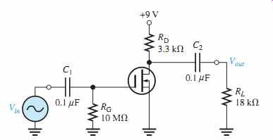
FIG. 61 22. Determine the total drain voltage waveform (dc and ac)
and the Vout waveform in FIG. 62.
gm = 4.8 mS and IDSS = 15 mA. Observe that VGS = 0.
FIG. 62
FIG. 63 VDD
23. For the unloaded amplifier in FIG. 63, find VGS, ID, VDS, and the rms output voltage Vds.
ID(on) = 8 mA at VGS = 12 V, VGS(th) = 4V, and gm = 4500 S.
Section 2--The Common-Drain Amplifier
24. For the source-follower in FIG. 64, determine the voltage gain and input resistance.
IGSS = 50 pA at VGS =-15 V and gm = 5500 mS.
FIG. 64
25. If the JFET in FIG. 64 is replaced with one having a gm of what are the gain and the input resistance with all other conditions the same?
26. Find the gain of each amplifier in FIG. 65.
27. Determine the voltage gain of each amplifier in FIG. 65 when the capacitively coupled load is changed to 10 k OHM.
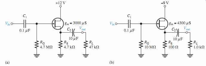
FIG. 65
Section 3--The Common-Gate Amplifier
28. A common-gate amplifier has a
What is its gain?
29. What is the input resistance of the amplifier in Problem 28?
30. Determine the voltage gain and input resistance of the common-gate amplifier in FIG. 66.
31. For a cascode amplifier like shown in FIG. 24,
If determine the voltage gain and the input impedance R3 = 15 M OHM and L = 1.5 mH, gm = 2800 mS, IGSS = 2 nA at VGS = 15 V.
gm = 4000 mS and Rd = 1.5 k OHM.
at f = 100 MHz.
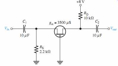
FIG. 66
Section 4--The Class D Amplifier
32. A class D amplifier has an output of If the input signal is 5 mV, what is the voltage gain?
33. A certain class D amplifier dissipates an internal power of 140 mW in the comparator and the triangular wave generator. Each complementary MOSFET has 0.25 V drop in the on state. The amplifier operates from dc sources and provides 0.35 A to a load. Determine the efficiency.
Section 5--MOSFET Analog Switching
34. An analog switch uses an n-channel MOSFET with VGS(th) = 4 V. A voltage of +8 V is applied to the gate. Determine the maximum peak-to-peak input signal that can be applied if the drain-to-source voltage drop is neglected.
35. An analog switch is used to sample a signal with a maximum frequency of 15 kHz. Determine the minimum frequency of the pulses applied to the MOSFET gate.
36. A switched-capacitor circuit uses a 10 pF capacitor. Determine the frequency required to emu late a resistor.
37. For a frequency of 25 kHz, what is the emulated resistance in a switched-capacitor circuit if Section 6 MOSFET Digital Switching
38. What is the output voltage of a CMOS inverter that operates with VDD =5 V, when the input is 0 V? When the input is +5 V?
39. For each of the following input combinations, determine the output of a CMOS NAND gate that operates with VDD=3.3 V.
(a) VA = 0 V, VB = 0 V
(b) VA =3.3 V, VB = 0 V
(c) VA = 0 V, VB =3.3 V
(d) VA =3.3 V, VB =3.3 V
40. Repeat Problem 39 for a CMOS NOR gate.
41. List two advantages of the MOSFET over the BJT in power switching.
C = 0.001 uF? 10 k OHM ;12 V ;9 V.
Section 7--Troubleshooting
42. What symptom(s) would indicate each of the following failures when a signal voltage is applied to the input in FIG. 67? (a) Q1 open from drain to source (b) R3 open (c) C2 shorted (d) C3 open (e) Q2 open from drain to source
43. If Vin = 10 mV rms in FIG. 67, what is Vout for each of the following faults? (a) C1 open (b) C4 open (c) a short from the source of Q2 to ground (d) Q2 has an open gate
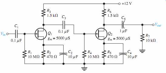
FIG. 67
DATASHEET PROBLEMS
44. What type of FET is the 2N3796?
45. Referring to the datasheet in FIG. 68, determine the following:
(a) typical VGS(off ) for the 2N3796 (b) maximum drain-to-source voltage for the 2N3797 (c) maximum power dissipation for the 2N3797 at an ambient temperature of (d) maximum gate-to-source voltage for the 2N3797
46. Referring to FIG. 68, determine the maximum power dissipation for a 2N3796 at an ambient temperature of
47. Referring to FIG. 68, determine the minimum gm0 for the 2N3796 at a frequency of 1 kHz.
48. What is the drain current when VGS = +3.5 V for the 2N3797?
49. Typically, what is the drain current for a zero-biased 2N3796?
50. What is the maximum possible voltage gain for a 2N3796 common-source amplifier with
ADVANCED PROBLEMS
51. The MOSFET in a certain single-stage common-source amplifier has a range of forward transconductance values from 2.5 mS to 7.5 mS. If the amplifier is capacitively coupled to a variable load that ranges from 4 k to and the dc drain resistance is determine the minimum and maximum voltage gains.
52. Design an amplifier using a 2N3797 that operates from a 24 V supply voltage. The typical dc drain-to-source voltage should be approximately 12 V and the typical voltage gain should be approximately 9.
53. Modify the amplifier you designed in Problem 52 so that the voltage gain can be set at 9 for any randomly selected 2N3797.
1.0 k OHM, 10 k OHM OHM Rd = 2.2 k OHM? 55°C. 25°C

FIG. 68 Partial datasheet for the 2N3796 and 2N3797 D-MOSFETs.