AMAZON multi-meters discounts AMAZON oscilloscope discounts
OUTLINE
1. Basic Concepts
2. The Decibel
3. Low-Frequency Amplifier Response
4. High-Frequency Amplifier Response
5.. Total Amplifier Frequency Response
6. Frequency Response of Multistage Amplifiers
GOALS
-- Explain how circuit capacitances affect the frequency response of an amplifier
-- Use the decibel (dB) to express amplifier gain
-- Analyze the low-frequency response of an amplifier
-- Analyze the high-frequency response of an amplifier
-- Analyze an amplifier for total frequency response
-- Analyze multistage amplifiers for frequency response
-- Measure the frequency response of an amplifier
TERMINOLOGY
-- Decibel
-- Midrange gain
-- Critical frequency
-- Roll-off
-- Decade
-- Bode Plot
-- Bandwidth
INTRODUCTION
In the previous Sections on amplifiers, the effects of the input frequency on an amplifier's operation due to capacitive elements in the circuit were neglected in order to focus on other concepts. The coupling and bypass capacitors were considered to be ideal shorts and the internal transistor capacitances were considered to be ideal opens. This treatment is valid when the frequency is in an amplifier's midrange.
As you know, capacitive reactance decreases with increasing frequency and vice versa. When the frequency is low enough, the coupling and bypass capacitors can no longer be considered as shorts because their reactances are large enough to have a significant effect. Also, when the frequency is high enough, the internal transistor capacitances can no longer be considered as opens because their reactances become small enough to have a significant effect on the amplifier operation. A complete picture of an amplifier's response must take into account the full range of frequencies over which the amplifier can operate.
In this Section, you will study the frequency effects on amplifier gain and phase shift. The coverage applies to both BJT and FET amplifiers, and a mix of both are included to illustrate the concepts.
1. BASIC CONCEPTS
In amplifiers, the coupling and bypass capacitors appear to be shorts to ac at the midband frequencies. At low frequencies the capacitive reactance of these capacitors affect the gain and phase shift of signals, so they must be taken into account. The frequency response of an amplifier is the change in gain or phase shift over a specified range of input signal frequencies.
Goals:
-- Explain how circuit capacitances affect the frequency response of an amplifier
-- Define frequency response
-- Discuss the effect of coupling capacitors
-- Recall the formula for capacitive reactance
-- Discuss the effect of bypass capacitors
-- Describe the effect of internal transistor capacitances
-- Identify the internal capacitance in BJTs and JFETs
-- Explain Miller's theorem
-- Calculate the Miller input and output capacitances
Effect of Coupling Capacitors
Recall from basic circuit theory that XC = 1/(2 pi fC).
This formula shows that the capacitive reactance varies inversely with frequency. At lower frequencies the reactance is greater, and it decreases as the frequency increases. At lower frequencies-for example, audio frequencies below 10 Hz-capacitively coupled amplifiers such as those in FIG. 1 have less voltage gain than they have at higher frequencies. The reason is that at lower frequencies more signal voltage is dropped across C1 and C3 because their reactances are higher.
This higher signal voltage drop at lower frequencies reduces the voltage gain. Also, a phase shift is introduced by the coupling capacitors because C1 forms a lead circuit with the Rin of the amplifier and C3 forms a lead circuit with RL in series with RC or RD. Recall that a lead circuit is an RC circuit in which the output voltage across R leads the input voltage in phase.
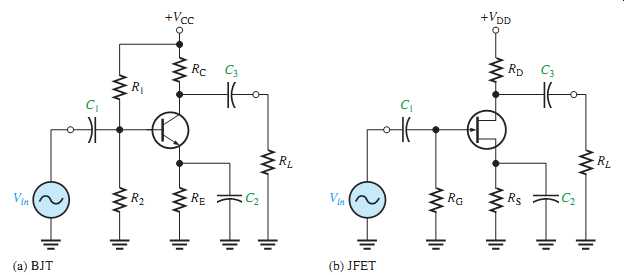
FIG. 1--Examples of capacitively coupled BJT and FET amplifiers.
Effect of Bypass Capacitors
At lower frequencies, the reactance of the bypass capacitor, C2 in FIG. 1, becomes significant and the emitter (or FET source terminal) is no longer at ac ground. The capacitive reactance XC2 in parallel with RE (or RS) creates an impedance that reduces the gain. This is illustrated in FIG. 2.
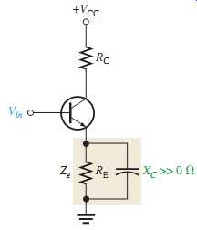
FIG. 2--Nonzero reactance of the bypass capacitor in parallel with RE
creates an emitter impedance, (Ze), which reduces the voltage gain.
Effect of Internal Transistor Capacitances
At high frequencies, the coupling and bypass capacitors become effective ac shorts and do not affect an amplifier's response. Internal transistor junction capacitances, however, do come into play, reducing an amplifier's gain and introducing phase shift as the signal frequency increases.
FIG. 3 shows the internal pn junction capacitances for both a bipolar junction transistor and a JFET. In the case of the BJT, Cbe is the base-emitter junction capacitance and Cbc is the base-collector junction capacitance. In the case of the JFET, Cgs is the capacitance between gate and source and Cgd is the capacitance between gate and drain.
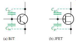
FIG. 3--Internal transistor capacitances.
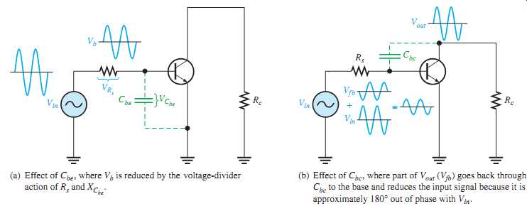
FIG. 4--AC equivalent circuit for a BJT amplifier showing effects of the
internal capacitances Cbe and Cbc.(a) Effect of Cbe, where Vb is reduced
by the voltage-divider action of Rs and XCbe; (b) Effect of Cbc, where
part of Vout (Vfb) goes back through Cbc to the base and reduces the input
signal because it is approximately 180° out of phase with Vin.
Datasheets often refer to the BJT capacitance Cbc as the output capacitance, often designated Cob. The capacitance Cbe is often designated as the input capacitance Cib.
Datasheets for FETs normally specify input capacitance Ciss and reverse transfer capacitance Crss. From these, Cgs and Cgd can be calculated, as you will see in Sect. 4.
At lower frequencies, the internal capacitances have a very high reactance because of their low capacitance value (usually only a few picofarads) and the low frequency value. There fore, they look like opens and have no effect on the transistor's performance. As the frequency goes up, the internal capacitive reactances go down, and at some point they begin to have a significant effect on the transistor's gain. When the reactance of Cbe (or Cgs) becomes small enough, a significant amount of the signal voltage is lost due to a voltage-divider effect of the signal source resistance and the reactance of Cbe, as illustrated in FIG. 4(a). When the reactance of Cbc (or Cgd) becomes small enough, a significant amount of output signal voltage is fed back out of phase with the input (negative feedback), thus effectively reducing the volt age gain. This is illustrated in FIG. 4(b).
Miller's Theorem
Miller's theorem is used to simplify the analysis of inverting amplifiers at high frequencies where the internal transistor capacitances are important. The capacitance Cbc in BJTs (Cgd in FETs) between the input (base or gate) and the output (collector or drain) is shown in FIG. 5(a) in a generalized form. Av is the absolute voltage gain of the inverting amplifier at midrange frequencies, and C represents either Cbc or Cgd.
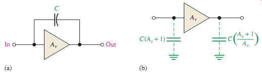
FIG. 5--General case of Miller input and output capacitances. C represents
Cbc or Cgd.
Miller's theorem states that C effectively appears as a capacitance from input to ground, as shown in FIG. 5(b), that can be expressed as follows:
EQN. 1 Cin(Miller) = C(Av + 1)
This formula shows that Cbc (or Cgd) has a much greater impact on input capacitance than its actual value. For example, if Cbc = 6 pF and the amplifier gain is 50, then Cin(Miller) =306 pF. FIG. 6 shows how this effective input capacitance appears in the actual ac equivalent circuit in parallel with Cbe (or Cgs).
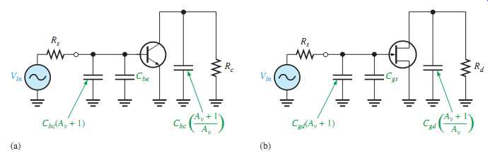
FIG. 6--Amplifier ac equivalent circuits showing internal capacitances
and effective Miller capacitances.
Miller's theorem also states that C effectively appears as a capacitance from output to ground, as shown in FIG. 5(b), that can be expressed as follows:

EQN. 2
This formula indicates that if the voltage gain is 10 or greater, Cout(Miller) is approximately equal to Cbc or Cgd because (Av = 1) Av is approximately equal to 1. FIG. 6 also shows how this effective output capacitance appears in the ac equivalent circuit for BJTs and FETs.
2. THE DECIBEL
The decibel is a unit of logarithmic gain measurement and is commonly used to express amplifier response.
Goals:
-- Use the decibel (dB) to express amplifier gain
-- Express power gain and voltage gain in dB
-- Discuss the 0 dB reference
-- Define midrange gain
-- Define and discuss the critical frequency
-- Discuss power measurement in dBm
-- Identify the internal capacitance in BJTs and JFETs
-- Explain Miller's theorem
-- Calculate the Miller input and output capacitances
The use of decibels to express gain was introduced in Section 6. The decibel unit is important in amplifier measurements. The basis for the decibel unit stems from the logarithmic response of the human ear to the intensity of sound. The decibel is a logarithmic measurement of the ratio of one power to another or one voltage to another. Power gain is expressed in decibels (dB) by the following formula:
EQN. 3: Ap(dB) = 10 log Ap
where Ap is the actual power gain, Pout Pin. Voltage gain is expressed in decibels by the following formula:
EQN. 4: Av (dB) = 20 log Av
If Av is greater than 1, the dB gain is positive. If Av is less than 1, the dB gain is negative and is usually called attenuation. You can use the LOG key on your calculator when working with these formulas.
FYI---The factor of 20 in EQN. 4 is because power is proportional to voltage squared. Technically, the equation should be applied only when the voltages are measured in the same impedance. This is the case for many communication systems, such as in television or microwave systems.
0 dB Reference
It is often convenient in amplifiers to assign a certain value of gain as the 0 dB reference.
This does not mean that the actual voltage gain is 1 (which is 0 dB); it means that the reference gain, no matter what its actual value, is used as a reference with which to compare other values of gain and is therefore assigned a 0 dB value.
Many amplifiers exhibit a maximum gain over a certain range of frequencies and a reduced gain at frequencies below and above this range. The maximum gain occurs for the range of frequencies between the upper and lower critical frequencies and is called the midrange gain, which is assigned a 0 dB value. Any value of gain below midrange can be referenced to 0 dB and expressed as a negative dB value. For example, if the midrange voltage gain of a certain amplifier is 100 and the gain at a certain frequency below midrange is 50, then this reduced voltage gain can be expressed as 20 log (50>100) = 20 log (0.5) =-6 dB. This indicates that it is 6 dB below the 0 dB reference. Halving the output voltage for a steady input voltage is always a 6 dB reduction in the gain. Correspondingly, a doubling of the output voltage is always a 6 dB increase in the gain. FIG. 7 illustrates a normalized gain-versus-frequency curve showing several dB points. The term normalized means that the midrange voltage gain is assigned a value of 1 or 0 dB.
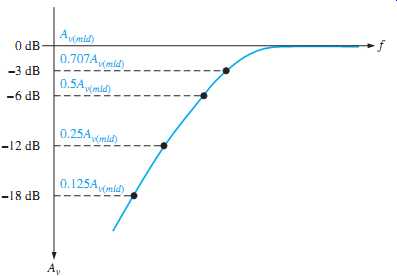
FIG. 7---Normalized voltage gain versus frequency curve.
TABLE 1 shows how doubling or halving voltage gains translates into decibel values.
Notice in the table that every time the voltage gain is doubled, the decibel value increases by 6 dB, and every time the gain is halved, the dB value decreases by 6 dB.
Critical Frequency
A critical frequency (also known as cutoff frequency or corner frequency) is a frequency at which the output power drops to one-half of its midrange value. This corresponds to a 3 dB reduction in the power gain, as expressed in dB by the following formula:
Ap(dB) = 10 log (0.5) =-3dB
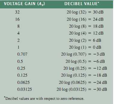
TABLE 1 Decibel values corresponding to doubling and halving of the voltage
gain.
Also, at the critical frequencies the voltage gain is 70.7% of its midrange value and is ex pressed in dB as Av(dB) = 20 log (0.707) = -3dB
FYI-----The unit of dBmV is used in some applications such as cable TV where the reference level is 1 mV, which corresponds to 0 dB. Just as the dBm is used to indicate actual power, the dBmV unit is used to indicate actual voltage.

TABLE 2 Power in terms of dBm.
Power Measurement in dBm
The dBm is a unit for measuring power levels referenced to 1 mW. Positive dBm values represent power levels above 1 mW, and negative dBm values represent power levels below 1 mW.
Because the decibel (dB) can be used to represent only power ratios, not actual power, the dBm provides a convenient way to express actual power output of an amplifier or other device. Each 3 dBm increase corresponds to a doubling of the power, and a 3 dBm de crease corresponds to a halving of the power.
To state that an amplifier has a 3 dB power gain indicates only that the output power is twice the input power and nothing about the actual output power. To indicate actual output power, the dBm can be used. For example, 3 dBm is equivalent to 2 mW because 2 mW is twice the 1 mW reference. 6 dBm is equivalent to 4 mW, and so on. Likewise, -3dBm is the same as 0.5 mW. TABLE 2 shows several values of power in terms of dBm.
3. LOW-FREQUENCY AMPLIFIER RESPONSE
The voltage gain and phase shift of capacitively coupled amplifiers are affected when the signal frequency is below a critical value. At low frequencies, the reactance of the coupling capacitors becomes significant, resulting in a reduction in voltage gain and an increase in phase shift. Frequency responses of both BJT and FET capacitively coupled amplifiers are discussed.
Goals:
-- Analyze the low-frequency response of an amplifier
-- Analyze a BJT amplifier
-- Calculate the midrange voltage gain
Identify the parts of the amplifier that affect low-frequency response
-- Identify and analyze the BJT amplifier's input RC circuit
-- Calculate the lower critical frequency and gain roll-off
Sketch a Bode plot
-- Define decade and octave
Determine the phase shift
-- Identify and analyze the BJT amplifier's output RC circuit
-- Calculate the lower critical frequency
Determine the phase shift
-- Identify and analyze the BJT amplifier's bypass RC circuit
-- Calculate the lower critical frequency
Explain the effect of a swamping resistor
-- Analyze a FET amplifier
-- Identify and analyze the D-MOSFET amplifier's input RC circuit
-- Calculate the lower critical frequency
Determine the phase shift
-- Identify and analyze the D-MOSFET amplifier's output RC circuit
-- Calculate the lower critical frequency
Determine the phase shift
-- Explain the total low-frequency response of an amplifier
-- Illustrate the response with Bode plots
-- Calculate the lower critical frequency
Determine the phase shift
BJT Amplifiers
A typical capacitively coupled common-emitter amplifier is shown in FIG. 8.
Assuming that the coupling and bypass capacitors are ideal shorts at the midrange signal frequency, you can determine the midrange voltage gain using EQN. 5, where Rc=Rc||RL .
EQN. 5 
If a swamping resistor is used, it appears in series with and the equation becomes r’e (RE1)
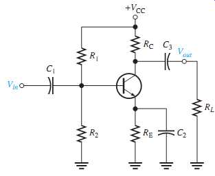
FIG. 8 A capacitively coupled BJT amplifier.
The BJT amplifier in FIG. 8 has three high-pass RC circuits that affect its gain as the frequency is reduced below midrange. These are shown in the low-frequency ac equivalent circuit in FIG. 9. Unlike the ac equivalent circuit used in previous Sections, which represented midrange response (XC = 0 ohm), the low-frequency equivalent circuit retains the coupling and bypass capacitors because XC is not small enough to neglect when the signal frequency is sufficiently low.
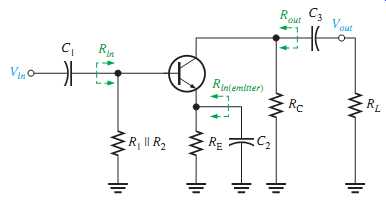
FIG. 9--The low-frequency ac equivalent circuit of the amplifier in FIG.
8 consists of three high-pass RC circuits.
One RC circuit is formed by the input coupling capacitor C1 and the input resistance of the amplifier. The second RC circuit is formed by the output coupling capacitor C3, the resistance looking in at the collector , and the load resistance. The third RC circuit that affects the low-frequency response is formed by the emitter-bypass capacitor C2 and the resistance looking in at the emitter.
The Input RC Circuit
The input RC circuit for the BJT amplifier in FIG. 8 is formed by C1 and the amplifier's input resistance and is shown in FIG. 10. (Input resistance was discussed in Section 6.) As the signal frequency decreases, XC1 increases. This causes less voltage across the input resistance of the amplifier at the base because more voltage is dropped across C1 and because of this, the overall voltage gain of the amplifier is reduced. The base voltage for the input RC circuit in FIG. 10 (neglecting the internal resistance of the input signal source) can be stated as (Rout)
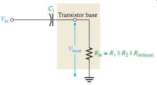
FIG. 10--Input RC circuit formed by the input coupling capacitor and
the amplifier's input resistance.
As previously mentioned, a critical point in the amplifier's response occurs when the output voltage is 70.7% of its midrange value. This condition occurs in the input RC circuit when XC1=Rin
Lower Critical Frequency
The condition where the gain is down 3 dB is logically called the -3 dB point of the amplifier response; the overall gain is 3 dB less than at midrange frequencies because of the attenuation (gain less than 1) of the input RC circuit. The frequency, fcl, at which this condition occurs is called the lower critical frequency (also known as the lower cutoff frequency, lower corner frequency, or lower break frequency) and can be calculated as follows:
EQN. 6 
If the resistance of the input source is taken into account, EQN. 6 becomes [...]
Voltage Gain Roll-Off at Low Frequencies
As you have seen, the input RC circuit reduces the overall voltage gain of an amplifier by 3 dB when the frequency is reduced to the critical value fc . As the frequency continues to decrease below fc, the overall voltage gain also continues to decrease. The rate of decrease in voltage gain with frequency is called roll-off.
For each ten times reduction in frequency below fc, there is a 20 dB reduction in voltage gain.
Let's consider a frequency that is one-tenth of the critical frequency( f = 0.1fc).
Since XC1=Rin at fc, then XC1=10Rin at 0.1fc because of the inverse relationship of XC1 and f.
The attenuation of the input RC circuit is, therefore,
[...]
The dB attenuation is [...]
The Bode Plot
A ten-times change in frequency is called a decade. So, for the input RC circuit, the attenuation is reduced by 20 dB for each decade that the frequency decreases below the critical frequency. This causes the overall voltage gain to drop 20 dB per decade.
A plot of dB voltage gain versus frequency on semilog graph paper (logarithmic horizontal axis scale and a linear vertical axis scale) is called a Bode plot. A generalized Bode plot for an input RC circuit appears in FIG. 12. The ideal response curve is shown in blue. Notice that it is flat (0 dB) down to the critical frequency, at which point the gain drops at -20 dB/decade as shown. Above fc are the midrange frequencies. The actual response curve is shown in red. Notice that it decreases gradually beginning in midrange and is down to -3dB at the critical frequency. Often, the ideal response is used to simplify amplifier analysis. As previously mentioned, the critical frequency at which the curve "breaks" into a -20 dB/decade drop is sometimes called the lower break frequency.
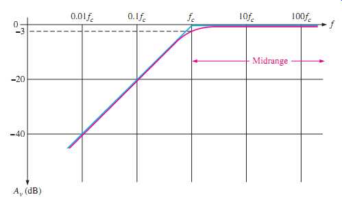
FIG. 12---Bode plot. (Blue is ideal; red is actual.)
Sometimes, the voltage gain roll-off of an amplifier is expressed in dB/octave rather than dB/decade. An octave corresponds to a doubling or halving of the frequency. For ex ample, an increase in frequency from 100 Hz to 200 Hz is an octave. Likewise, a decrease in frequency from 100 kHz to 50 kHz is also an octave. A rate of -20 dB/decade is approximately equivalent to -6 dB/octave, a rate of -40 dB/decade is approximately equivalent to -12 dB/octave, and so on.
-------
FROM HISTORY
Hendrik Wade Bode pronounced Boh-dee (1905-1982) was born in Madison, Wisconsin. He received his B.A. degree in 1924, at the age of 19, from Ohio State University and his M.A. degree in 1926, both in Mathematics. He was hired by Bell Labs and completed his Ph.D. in Physics in 1935. In 1938 he developed his now well-known magnitude and phase plots. His work on automatic control systems introduced innovative methods to the study of system stability.
-------
Phase Shift in the Input RC Circuit
In addition to reducing the voltage gain, the input RC circuit also causes an increasing phase shift through an amplifier as the frequency decreases. At midrange frequencies, the phase shift through the input RC circuit is approximately zero because the capacitive reactance, XC1, is approximately 0 ohm. At lower frequencies, higher values of XC1 cause a phase shift to be introduced, and the output volt age of the RC circuit leads the input voltage. As you learned in ac circuit theory, the phase angle in an input RC circuit is expressed as:
Eqn 7 
A continuation of this analysis will show that the phase shift through the input RC circuit approaches as the frequency approaches zero. A plot of phase angle versus frequency is shown in Figure 13. The result is that the voltage at the base of the transistor leads the input signal voltage in phase below midrange, as shown in Figure 14.
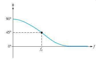
FIG. 13---Phase angle versus frequency for the input RC circuit.
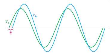
FIG. 14---The input RC circuit causes the base voltage to lead the input
voltage below midrange by an amount equal to the circuit phase angle, theta.
The Output RC Circuit
The second high-pass RC circuit in the BJT amplifier of Figure 8 is formed by the coupling capacitor C3, the resistance looking in at the collector, and the load resistance RL1 as shown in Figure 15(a). In determining the output resistance, looking in at the collector, the transistor is treated as an ideal current source (with infinite internal resistance), and the upper end of RC is effectively at ac ground, as shown in Figure 15(b). Therefore, thevenizing the circuit to the left of capacitor C3 produces an equivalent voltage source equal to the collector voltage and a series resistance equal to RC, as shown in Figure 15(c). The lower critical frequency of this output RC circuit is
Equation 8 
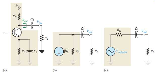
FIG. 15--Development of the equivalent low-frequency output RC circuit.
The effect of the output RC circuit on the amplifier voltage gain is similar to that of the input RC circuit. As the signal frequency decreases, XC3 increases. This causes less voltage across the load resistance because more voltage is dropped across C3. The signal voltage is reduced by a factor of 0.707 when frequency is reduced to the lower critical value, fcl, for the circuit. This corresponds to a 3 dB reduction in voltage gain.
Phase Shift in the Output RC Circuit
The phase angle in the output RC circuit is
EQN. 9 
theta = 0 degr. for the midrange frequencies and approaches 90 deg as the frequency approaches zero (XC3 approaches infinity). At the critical frequency fc, the phase shift is 45 deg.
The Bypass RC Circuit
The third RC circuit that affects the low-frequency gain of the BJT amplifier in FIG. 8 includes the bypass capacitor C2. As illustrated in FIG. 17(a) for midrange frequencies, it is assumed that XC2 = 0 ohm, effectively shorting the emitter to ground so that the amplifier gain is Rc>r’ e, as you already know. As the frequency is reduced, XC2 increases and no longer provides a sufficiently low reactance to effectively place the emitter at ac ground, as shown in part (b). Because the impedance from emitter to ground increases, the gain decreases. In this case, Re in the formula Av = Rc>(r’e + Re), is replaced by an impedance formed by RE in parallel with XC2.
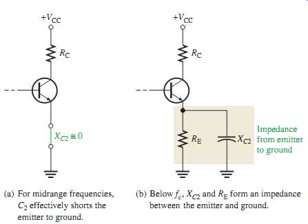
FIG. 17--At low frequencies, XC2 in parallel with RE creates an impedance
that reduces the voltage gain.
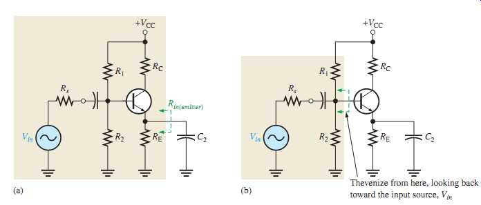
FIG. 18 Development of the equivalent bypass RC circuit.
The bypass RC circuit is formed by C2 and the resistance looking in at the emitter, Rin(emitter), as shown in FIG. 18(a). The resistance looking in at the emitter is derived as follows. First, Thevenin's theorem is applied looking from the base of the transistor toward the input source Vin, as shown in FIG. 18(b). This results in an equivalent resistance (Rth) and an equivalent voltage source (Vth(1)) in series with the base, as shown in FIG. 18(c). The resistance looking in at the emitter is determined with the equivalent input source shorted, as shown in FIG. 18(d), and is expressed as follows:
EQN. 10
Looking from the capacitor is in parallel with RE, as shown in FIG. 18(e). Thevenizing again, we get the equivalent RC circuit shown in FIG. 18(f).
The lower critical frequency for this equivalent bypass RC circuit is C2, r’e + Rth>Beta_ac 1
EQN. 11
FET Amplifiers
A zero-biased D-MOSFET amplifier with capacitive coupling on the input and output is shown in FIG. 20. As you learned in Section 9, the midrange voltage gain of a zero biased amplifier is
Av(mid ) = gmRd
This is the gain at frequencies high enough so that the capacitive reactances are approximately zero.
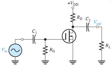
FIG. 20 Zero-biased D-MOSFET amplifier.
The amplifier in FIG. 20 has only two high-pass RC circuits that influence its low frequency response. One RC circuit is formed by the input coupling capacitor C1 and the input resistance. The other circuit is formed by the output coupling capacitor C2 and the output resistance looking in at the drain.
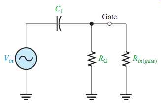
FIG. 21--Input RC circuit.
The Input RC Circuit
The input RC circuit for the FET amplifier in FIG. 20 is shown in FIG. 21. As in the case for the BJT amplifier, the reactance of the input coupling capacitor increases as the frequency decreases. When XC1 Rin, the gain is down 3 dB below its midrange value.
The lower critical frequency is
The input resistance is
where Rin(gate) is determined from datasheet information as
For practical work, the value of is so large it can be ignored, as will be illustrated in EX. 7.
The gain rolls off below fc at 20 dB/decade, as previously shown. The phase angle in the low-frequency input RC circuit is
Rin(gate)

EQN. 12
EQN. 13
The Output RC Circuit
The second RC circuit that affects the low-frequency response of the FET amplifier in FIG. 20 is formed by a coupling capacitor C2 and the output resistance looking in at the drain, as shown in FIG. 23(a). The load resistor, RL, is also included. As in the case of the BJT, the FET is treated as a current source, and the upper end of RD is effectively ac ground, as shown in FIG. 23(b). The Thevenin equivalent of the circuit to the left of C is shown in FIG. 23(c). The lower critical frequency for this RC circuit is

EQN. 14
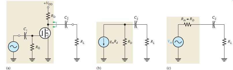
FIG. 23 Development of the equivalent low-frequency output RC circuit.
The effect of the output RC circuit on the amplifier's voltage gain below the midrange is similar to that of the input RC circuit. The circuit with the highest critical frequency dominates because it is the one that first causes the gain to roll off as the frequency drops below its midrange values. The phase angle in the low-frequency output RC circuit is:
EQN. 15 
Again, at the critical frequency, the phase angle is 45° and approaches 90° as the frequency approaches zero. However, starting at the critical frequency, the phase angle 45° decreases from and becomes very small as the frequency goes higher.
Total Low-Frequency Response of an Amplifier
Now that we have individually examined the high-pass RC circuits that affect a BJT or FET amplifier's voltage gain at low frequencies, let's look at the combined effect of the three RC circuits in a BJT amplifier. Each circuit has a critical frequency determined by the R and C values. The critical frequencies of the three RC circuits are not necessarily all equal. If one of the RC circuits has a critical (break) frequency higher than the other two, then it is the dominant RC circuit. The dominant circuit determines the frequency at which the overall voltage gain of the amplifier begins to drop at -20 dB/decade. The other circuits each cause an additional -20 dB/decade roll-off below their respective critical (break) frequencies.
To get a better picture of what happens at low frequencies, refer to the Bode plot in FIG. 25, which shows the superimposed ideal responses for the three RC circuits (green lines) of a BJT amplifier. In this example, each RC circuit has a different critical frequency. The input RC circuit is dominant (highest fc) in this case, and the bypass RC circuit has the lowest fc. The ideal overall response is shown as the blue line.
Here is what happens. As the frequency is reduced from midrange, the first "break point" occurs at the critical frequency of the input RC circuit, fcl(input), and the gain begins to drop at This constant roll-off rate continues until the critical frequency of the output RC circuit, fcl(output), is reached. At this break point, the output RC circuit adds another -20 dB/decade to make a total roll-off of -40 dB/decade. This constant -40 dB/decade roll-off continues until the critical frequency of the bypass RC circuit, fcl(bypass), is reached. The bypass RC circuit adds still another dB/decade at this break point, making the gain roll-off at -60 dB/decade.
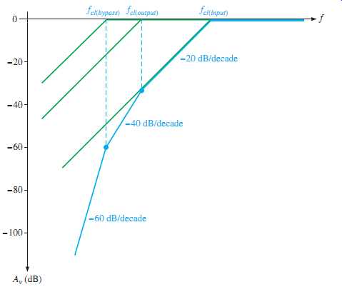
FIG. 25 Composite Bode plot of a BJT amplifier response for three low-frequency
RC circuits with different critical frequencies. Total response is shown
by the blue curve.
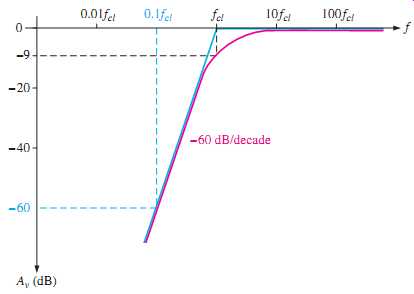
FIG. 26 Composite Bode plot of an amplifier response where all RC circuits
have the same fcl. (Blue is ideal; red is actual.)
If all RC circuits have the same critical frequency, the response curve has one break point at that value of fcl, and the voltage gain rolls off at -60 dB/decade below that value, as shown by the ideal curve (blue) in FIG. 26. Actually, the midrange voltage gain does not extend down to the dominant critical frequency but is really at -9dB below the midrange voltage gain at that point (-3 dB for each RC circuit), as shown by the red curve.
FYI---SPICE was one of the first computer programs that could simulate electronic circuits. Its origins can be traced to a program called CANCER (Computer Analysis of Nonlinear Circuits, Excluding Radiation) at the University of California. It was developed as a computer aid for designing integrated circuits in the 1960s. SPICE is an acronym for Simulation Program with Integrated Circuit Emphasis. Over the years, SPICE has been revised many times but is still the underlying software for many of today's simulations.
Computer Simulation of Frequency Response
As you saw in the previous example, the calculation of multiple critical frequencies is involved and each critical frequency contributes to the overall response. The ideal response shown in EX. 9 is an excellent first approximation, but when more accuracy is required, a computer simulation is used. The computer takes into account all of the parameters for the particular device including effects such as internal capacitances that are usually ignored in manual calculations, and it can calculate in detail the interactions that occur when there are multiple breakpoints as in EX. 9.
Multisim is based on SPICE models that can show the frequency response of circuits on the Bode plotter. As mentioned earlier, the Bode plotter is not a real instrument. It performs the same function as an instrument called the spectrum analyzer, which can also plot the frequency response of a circuit. EX. 10 illustrates the application of computer analysis to the circuit in the previous example.