AMAZON multi-meters discounts AMAZON oscilloscope discounts
4. HIGH-FREQUENCY AMPLIFIER RESPONSE
You have seen how the coupling and bypass capacitors affect the voltage gain of an amplifier at lower frequencies where the reactances of the coupling and bypass capacitors are significant. In the midrange of an amplifier, the effects of the capacitors are minimal and can be neglected. If the frequency is increased sufficiently, a point is reached where the transistor's internal capacitances begin to have a significant effect on the gain. The basic differences between BJTs and FETs are the specifications of the internal capacitances and the input resistance.
Goals:
-- Analyze the high-frequency response of an amplifier
-- Analyze a BJT amplifier
-- Apply Miller's theorem
-- Identify and analyze the BJT amplifier's input RC circuit
-- Calculate the upper critical frequency and gain roll-off
Determine the phase shift
-- Identify and analyze the BJT amplifier's output RC circuit
-- Calculate the upper critical frequency
Determine the phase shift
-- Analyze a FET amplifier
-- Identify and analyze a JFET amplifier
-- Determine internal capacitances on a datasheet
Apply Miller's theorem
-- Identify and analyze the JFET amplifier's input RC circuit
-- Calculate the upper critical frequency
Determine the phase shift
-- Identify and analyze the JFET amplifier's output RC circuit
-- Calculate the upper critical frequency
Determine the phase shift
-- Discuss the total high-frequency response of an amplifier
-- Use Bode plots to illustrate the high-frequency response
BJT Amplifiers

FIG. 31 Capacitively coupled amplifier and its high-frequency equivalent
circuit.

FIG. 32 High-frequency equivalent circuit after applying Miller's theorem.
A high-frequency ac equivalent circuit for the BJT amplifier in FIG. 31(a) is shown in FIG. 31(b). Notice that the coupling and bypass capacitors are treated as effective shorts and do not appear in the equivalent circuit. The internal capacitances, Cbe and Cbc, which are significant only at high frequencies, do appear in the diagram. As previously mentioned, Cbe is sometimes called the input capacitance Cib, and Cbc is sometimes called the output capacitance Cob. Cbe is specified on datasheets at a certain value of VBE. Often, a datasheet will list Cib as Cibo and Cob as Cobo. The "o" as the last letter in the subscript indicates the capacitance is measured with the base open. For example, a 2N2222A transistor has a Cbe of 25 pF at VBE=0.5 V dc, IC = 0, and f = 1 MHz. Also, Cbc is specified at a certain value of VBC. The 2N2222A has a maximum Cbc of 8 pF at VBC= 10 V dc.
Miller's Theorem in High-Frequency Analysis
By applying Miller's theorem to the inverting amplifier in FIG. 31(b) and using the midrange voltage gain, you have a circuit that can be analyzed for high-frequency response. Looking in from the signal source, the capacitance Cbc appears in the Miller input capacitance from base to ground.
Cin(Miller) = Cbc (Av + 1)
Cbe simply appears as a capacitance to ac ground, as shown in FIG. 32, in parallel with Cin(Miller). Looking in at the collector, Cbc appears in the Miller output capacitance from collector to ground. As shown in FIG. 32, the Miller output capacitance appears in parallel with Rc.
Cout(Miller) = Cbc ( Av + 1 / Av )
These two Miller capacitances create a high-frequency input RC circuit and a high frequency output RC circuit. These two circuits differ from the low-frequency input and output circuits, which act as high-pass filters, because the capacitances go to ground and therefore act as low-pass filters. The equivalent circuit in FIG. 32 is an ideal model because stray capacitances that are due to circuit interconnections are neglected.
The Input RC Circuit
At high frequencies, the input circuit is as shown in FIG. 33(a), where Beta_ac r’e is the input resistance at the base of the transistor because the bypass capacitor effectively shorts the emitter to ground. By combining Cbe and Cin (Miller) in parallel and repositioning, you get the simplified circuit shown in FIG. 33(b). Next, by thevenizing the circuit to the left of the capacitor, as indicated, the input RC circuit is reduced to the equivalent form shown in FIG. 33(c).
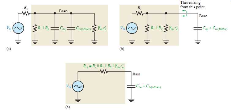
FIG. 33 Development of the equivalent high-frequency input RC circuit.
As the frequency increases, the capacitive reactance becomes smaller. This causes the signal voltage at the base to decrease, so the amplifier's voltage gain decreases. The reason for this is that the capacitance and resistance act as a voltage divider and, as the frequency increases, more voltage is dropped across the resistance and less across the capacitance. At the critical frequency, the gain is 3 dB less than its midrange value. The upper critical high frequency of the input circuit, fcu (input ), is the frequency at which the capacitive reactance is equal to the total resistance.
EQN. 16
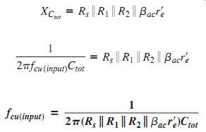
where Rs is the resistance of the signal source and Ctot = Cbe + Cin(Miller). As the frequency goes above fcu(input), the input RC circuit causes the gain to roll off at a rate of -20 dB/decade just as with the low-frequency response.
Phase Shift of the Input RC Circuit
Because the output voltage of a high-frequency input RC circuit is across the capacitor, the output of the circuit lags the input. The phase angle is expressed as:
EQN. 17

At the critical frequency, the phase angle is 45° with the signal voltage at the base of the transistor lagging the input signal. As the frequency increases above fc, the phase angle in creases above 45° and approaches 90° when the frequency is sufficiently high.
The Output RC Circuit
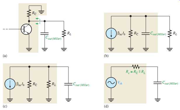
FIG. 36 Development of the equivalent high-frequency output RC circuit.
The high-frequency output RC circuit is formed by the Miller output capacitance and the resistance looking in at the collector, as shown in FIG. 36(a). In determining the out put resistance, the transistor is treated as a current source (open) and one end of RC is effectively ac ground, as shown in FIG. 36(b). By rearranging the position of the capacitance in the diagram and thevenizing the circuit to the left, as shown in FIG. 36(c), you get the equivalent circuit in FIG. 36(d). The equivalent output RC circuit consists of a resistance equal to the parallel combination of RC and RL in series with a capacitance that is determined by the following Miller formula:
If the voltage gain is at least 10, this formula can be approximated as
The upper critical frequency for the output circuit is determined with the following equation, where Rc = RC || RL.
EQN. 18

Just as in the input RC circuit, the output RC circuit reduces the gain by 3 dB at the critical frequency. When the frequency goes above the critical value, the gain drops at a rate. The phase angle introduced by the output RC circuit is -20 dB/decade
EQN. 19

FET Amplifiers
The approach to the high-frequency analysis of a FET amplifier is similar to that of a BJT amplifier. The basic differences are the specifications of the internal FET capacitances and the determination of the input resistance.
FIG. 39(a) shows a JFET common-source amplifier that will be used to illustrate high-frequency analysis. A high-frequency equivalent circuit for the amplifier is shown in FIG. 39(b). Notice that the coupling and bypass capacitors are assumed to have negligible reactances and are considered to be shorts. The internal capacitances Cgs and Cgd appear in the equivalent circuit because their reactances are significant at high frequencies.
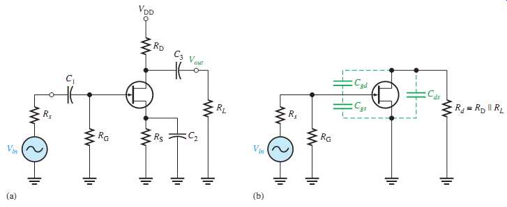
FIG. 39 Example of a JFET amplifier and its high-frequency equivalent
circuit.
Values of Cgs, Cgd, and Cds
FET datasheets do not normally provide values for Cgs, Cgd, or Cds. Instead, three other values are usually specified because they are easier to measure.
These are Ciss, the input capacitance; Crss, the reverse transfer capacitance; and Coss, the output capacitance. Because of the manufacturer's method of measurement, the following relationships allow you to determine the capacitor values needed for analysis.
EQN. 20; EQN. 21; EQN. 22 shown here:
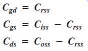
Coss is not specified as often as the other values on datasheets. Sometimes, it is designated as Cd (sub), the drain-to-substrate capacitance. In cases where a value is not available, you must either assume a value or neglect Cds.
Using Miller's Theorem
Miller's theorem is applied the same way in FET inverting amplifier high-frequency analysis as was done in BJT amplifiers. Looking in from the signal source in FIG. 39(b), Cgd effectively appears in the Miller input capacitance, which was given in EQN. 1, as follows:
Cin (Miller) = Cgd (Av + 1)
Cgs simply appears as a capacitance to ac ground in parallel with Cin(Miller), as shown in FIG. 40. Looking in at the drain, Cgd effectively appears in the Miller output capacitance (from EQN. 2) from drain to ground in parallel with Rd, as shown in FIG. 40.
Cout(Miller) = Cgd ( Av + 1 / Av )
These two Miller capacitances contribute to a high-frequency input RC circuit and a high frequency output RC circuit. Both are low-pass filters, which produce phase lag.

FIG. 40 High-frequency equivalent circuit after applying Miller's theorem.

FIG. 41 Input RC circuit.
The Input RC Circuit
The high-frequency input circuit forms a low-pass type of filter and is shown in FIG. 41(a). Because both RG and the input resistance at the gate of FETs are extremely high, the controlling resistance for the input circuit is the resistance of the input source as long as Rs << Rin.
This is because Rs appears in parallel with Rin when Thevenin's theorem is applied. The simplified input RC circuit appears in FIG. 41(b). The upper critical frequency for the input circuit is
EQN. 23

where Ctot Cgs Cin(Miller ). The input RC circuit produces a phase angle of
EQN. 24

The effect of the input RC circuit is to reduce the midrange gain of the amplifier by 3 dB at the critical frequency and to cause the gain to decrease at -20 dB/decade above fc.
The Output RC Circuit
The high-frequency output RC circuit is formed by the Miller output capacitance and the output resistance looking in at the drain, as shown in FIG. 43(a). As in the case of the BJT, the FET is treated as a current source. When you apply Thevenin's theorem, you get an equivalent output RC circuit consisting of RD in parallel with RL and an equivalent output capacitance.
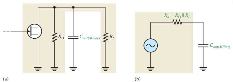
FIG. 43 Output RC circuit.
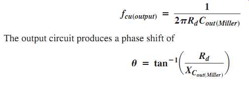
This equivalent output circuit is shown in FIG. 43(b). The critical frequency of the output RC lag circuit is
EQN. 25, EQN. 26, shown below:
Total High-Frequency Response of an Amplifier
As you have seen, the two RC circuits created by the internal transistor capacitances influence the high-frequency response of both BJT and FET amplifiers. As the frequency increases and reaches the high end of its midrange values, one of the RC circuits will cause the amplifier's gain to begin dropping off. The frequency at which this occurs is the dominant upper critical frequency; it is the lower of the two upper critical high frequencies. An ideal high-frequency Bode plot is shown in FIG. 44(a). It shows the first break point at fcu(input) where the voltage gain begins to roll off at -20 dB/decade. At fcu(output), the gain begins dropping at -40 dB/decade because each RC circuit is providing a -20 dB/decade roll-off. FIG. 44(b) shows a nonideal Bode plot where the voltage gain is actually -3 dB/decade below midrange at fcu(input). Other possibilities are that the output RC circuit is dominant or that both circuits have the same critical frequency.

FIG. 44 High-frequency Bode plots.
5. TOTAL AMPLIFIER FREQUENCY RESPONSE
In the previous sections, you learned how each RC circuit in an amplifier affects the frequency response. In this section, we will bring these concepts together and examine the total response of typical amplifiers and the specifications relating to their performance.
Goals:
-- Analyze an amplifier for total frequency response
-- Discuss bandwidth
-- Define the dominant critical frequencies
-- Explain gain-bandwidth product
-- Define unity-gain frequency
FIG. 45(b) shows a generalized ideal response curve (Bode plot) for the BJT amplifier shown in FIG. 45(a). As previously discussed, the three break points at the lower critical frequencies ( fcl1, fcl2, and fcl3) are produced by the three low-frequency RC circuits formed by the coupling and bypass capacitors. The break points at the upper critical frequencies, fcu1 and fcu2, are produced by the two high-frequency RC circuits formed by the transistor's internal capacitances.
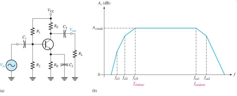
FIG. 45 A BJT amplifier and its generalized ideal response curve (Bode
plot).
Of particular interest are the two dominant critical frequencies, fcl3 and fcu1, in FIG. 45(b). These two frequencies are where the voltage gain of the amplifier is 3 dB below its midrange value. These dominant frequencies are designated fcl(dom) and fcu(dom).
The upper and lower dominant critical frequencies are sometimes called the half-power frequencies. This term is derived from the fact that the output power of an amplifier at its critical frequencies is one-half of its midrange power, as previously mentioned. This can be shown as follows, starting with the fact that the output voltage is 0.707 of its midrange value at the dominant critical frequencies.
Bandwidth
An amplifier normally operates with signal frequencies between fcl(dom) and fcu(dom). As you know, when the input signal frequency is at fcl(dom) or fcu(dom), the output signal voltage level is 70.7% of its midrange value or -3 dB. If the signal frequency drops below fcl(dom), the gain and thus the output signal level drops at 20 dB/decade until the next critical frequency is reached. The same occurs when the signal frequency goes above fcu(dom).
The range (band) of frequencies lying between fcl(dom) and fcu(dom) is defined as the bandwidth of the amplifier, as illustrated in FIG. 46. Only the dominant critical frequencies appear in the response curve because they determine the bandwidth. Also, some times the other critical frequencies are far enough away from the dominant frequencies that they play no significant role in the total amplifier response and can be neglected. The amplifier's bandwidth is expressed in units of hertz as
EQN. 27

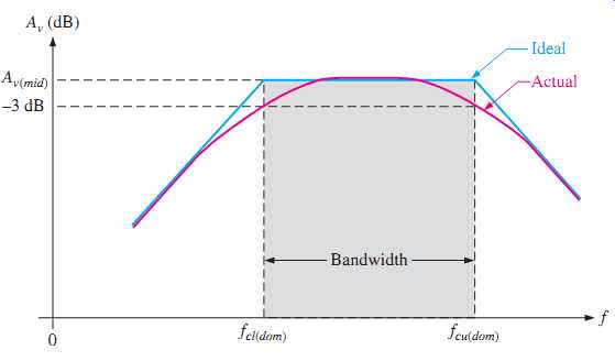
FIG. 46 Response curve illustrating the band width of an amplifier.
Ideally, all signal frequencies lying in an amplifier's bandwidth are amplified equally. For example, if a 10 mV rms signal is applied to an amplifier with a voltage gain of 20, it is amplified to 200 mV rms for all frequencies in the bandwidth. Actually, the gain is down 3 dB at fcl(dom) and fcu(dom).
Gain-Bandwidth Product
One characteristic of amplifiers is that the product of the voltage gain and the bandwidth is always constant when the roll-off is -20 dB/decade.
This characteristic is called the gain bandwidth product. Let's assume that the dominant lower critical frequency of a particular amplifier is much less than the dominant upper critical frequency.
fcu fcl(dom) << fcu(dom)
The bandwidth can then be approximated as
BW = fcu(dom) - fcl(dom) = fcu
Unity-Gain Frequency
The simplified Bode plot for this condition is shown in FIG. 47. Notice that fcl(dom) is neglected because it is so much smaller than fcu(dom), and the bandwidth approximately equals fcu(dom). Beginning at fcu(dom), the gain rolls off until unity gain (0 dB) is reached. The frequency at which the amplifier's gain is 1 is called the unity gain frequency, fT. The significance of fT is that it always equals the midrange voltage gain times the bandwidth and is constant for a given transistor.
EQN. 28

For the case shown in FIG. 47, fT=Av(mid) fcu(dom). For example, if a transistor datasheet specifies fT=100 MHz, this means that the transistor is capable of producing a voltage gain of 1 up to 100 MHz, or a gain of 100 up to 1 MHz, or any combination of gain and bandwidth that produces a product of 100 MHz.
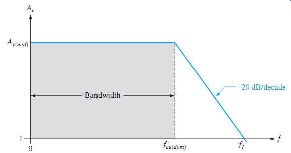
FIG. 47 Simplified response curve where fcl(dom) is negligible (assumed
to be zero) compared to fcu(dom).
6. FREQUENCY RESPONSE OF MULTISTAGE AMPLIFIERS
To this point, you have seen how the voltage gain of a single-stage amplifier changes over frequency. When two or more stages are cascaded to form a multistage amplifier, the overall frequency response is determined by the frequency response of each stage depending on the relationships of the critical frequencies.
Goals:
-- Analyze multistage amplifiers for frequency response
-- Analyze the case where the stages have different critical frequencies
-- Determine the overall bandwidth
-- Analyze the case where the stages have equal critical frequencies
-- Determine the overall bandwidth
When amplifier stages are cascaded to form a multistage amplifier, the dominant frequency response is determined by the responses of the individual stages. There are two cases to consider:
1. Each stage has a different dominant lower critical frequency and a different dominant upper critical frequency.
2. Each stage has the same dominant lower critical frequency and the same dominant upper critical frequency.
Different Critical Frequencies
Ideally, when the dominant lower critical frequency, fcl(dom), of each amplifier stage is different from the other stages, the overall dominant lower critical frequency, equals the dominant critical frequency of the stage with the highest fcl(dom).
Ideally, when the dominant upper critical frequency, fcu(dom), of each amplifier stage is different from the other stages, the overall dominant upper critical frequency, equals the dominant critical frequency of the stage with the lowest fcu(dom).
In practice, the critical frequencies interact, so these calculated values should be considered approximations that are useful for troubleshooting or estimating the response.
When more accuracy is required, a computer simulation is the best solution.
Overall Bandwidth
The bandwidth of a multistage amplifier is the difference between the overall dominant lower critical frequency and the overall dominant upper critical frequency.
BW = f ‘ cu(dom) - f ‘ cl(dom)
Equal Critical Frequencies
When each amplifier stage in a multistage arrangement has equal dominant critical frequencies, you may think that the overall dominant critical frequency is equal to the critical frequency of each stage. This is not the case, however.
When the dominant lower critical frequencies of each stage in a multistage amplifier are all the same, the overall dominant lower critical frequency is increased by a factor of (1__/2^1/n -1 )
as shown by the following formula (n is the number of stages in the multistage amplifier):
EQN. 29

When the dominant upper critical frequencies of each stage are all the same, the overall dominant upper critical frequency is reduced by a factor of√2^1/n -1.
EQN. 30

Computer Simulation for Multistage Amplifiers
With multistage amplifiers, the detailed calculation of the frequency response is greatly simplified by computer simulation. There are several interactions within each stage and other interactions between the stages that affect the overall response. When you need more accuracy, a computer simulation is used. This is particularly useful in design work because you can change a component and see the effect immediately on the frequency response. The following example illustrates the application of computer analysis to a multistage amplifier.
7. FREQUENCY RESPONSE MEASUREMENTS
Two basic methods are used to measure the frequency response of an amplifier. The methods apply to both BJT and FET amplifiers although a BJT amplifier is used as an example. You will concentrate on determining the two dominant critical frequencies. From these values, you can get the bandwidth.
Goals:
-- Measure the frequency response of an amplifier
-- Analyze the case where the stages have different critical frequencies
-- Determine the overall bandwidth
-- Analyze the case where the stages have equal critical frequencies
-- Determine the overall bandwidth
-- Measure the frequency response of an amplifier
-- Describe a general measurement procedure
-- Apply frequency/amplitude measurement to determine critical frequencies
-- Use step-response measurement
-- Determine the upper critical frequency
Determine the lower critical frequency
Frequency/Amplitude Measurement
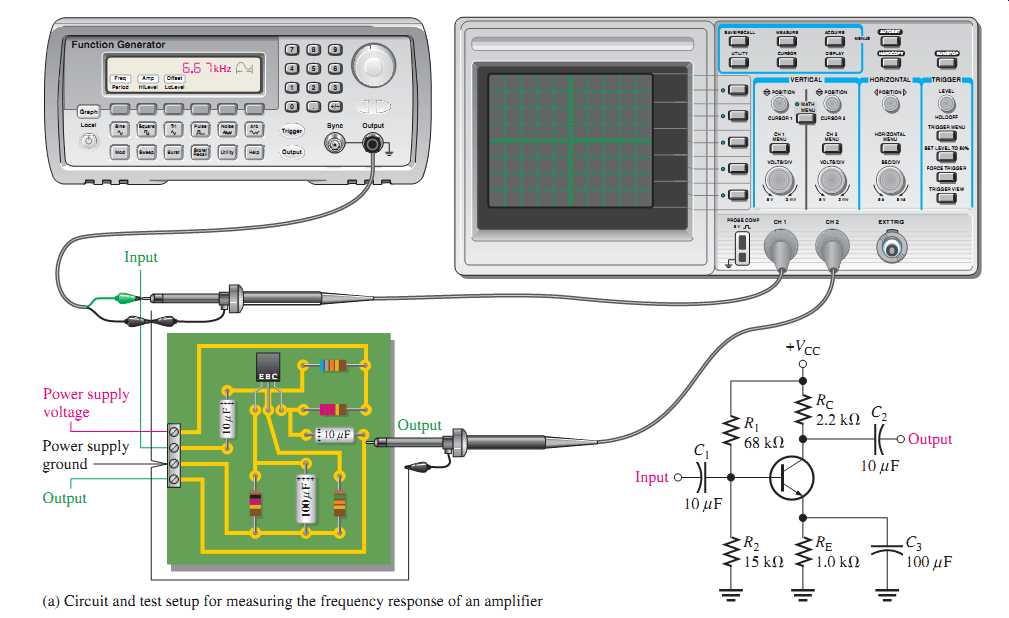
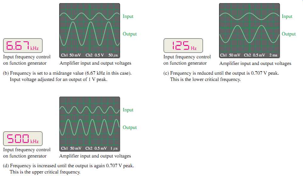
FIG. 50 A general procedure for measuring an amplifier's frequency response.
FIG. 50(a) shows the test setup for an amplifier circuit board. The schematic for the circuit board is also shown. The amplifier is driven by a sinusoidal voltage source with a dual-channel oscilloscope connected to the input and to the output. The input frequency is set to a midrange value, and its amplitude is adjusted to establish an output signal reference level, as shown in FIG. 50(b). This output voltage reference level for midrange should be set at a convenient value within the linear operation of the amplifier: for example, 100 mV, 1 V, 10 V, and so on. In this case, set the output signal to a peak value of 1 V.
Next, the frequency of the input voltage is decreased until the peak value of the output drops to 0.707 V. The amplitude of the input voltage must be kept constant as the frequency is reduced. Readjustment may be necessary because of changes in loading of the voltage source with frequency. When the output is 0.707 V, the frequency is measured, and you have the value for fcl as indicated in FIG. 50(c).
Next, the input frequency is increased back up through midrange and beyond until the peak value of the output voltage again drops to 0.707 V. Again, the amplitude of the input must be kept constant as the frequency is increased. When the output is 0.707 V, the frequency is measured and you have the value for fcu as indicated in FIG. 50(d).
From these two frequency measurements, you can find the bandwidth by the formula
BW = fcu - fcl.
Step-Response Measurement
The lower and upper critical frequencies of an amplifier can be determined using the step response method by applying a voltage step to the input of the amplifier and measuring the rise and fall times of the resulting output voltage. The basic test setup shown in FIG. 50(a) is used except that the pulse output of the function generator is selected. The input step is created by the rising edge of a pulse that has a long duration compared to the rise and fall times to be measured. The rise time of the input pulse must be fast compared to the rise time you measure from the amplifier.
High-Frequency Measurement
When a step input is applied, the amplifier's high frequency RC circuits (internal capacitances) prevent the output from responding immediately to the step input. As a result, the output voltage has a rise time (tr) associated with it, as shown in FIG. 51(a). In fact, the rise time is inversely related to the upper critical frequency (fcu) of the amplifier. As fcu becomes lower, the rise time of the output becomes greater. The oscilloscope display illustrates how the rise time is measured from the 10% amplitude point to the 90% amplitude point. The scope must be set on a short time base so the relatively short interval of the rise time can be accurately observed. Once this measurement is made, fcu can be calculated with the following formula:
EQN. 31

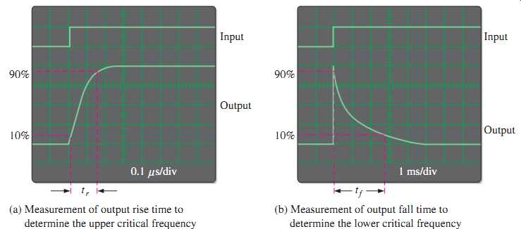
FIG. 51 Measurement of the rise and fall times associated with the amplifier's
step response. The outputs are inverted.
Low-Frequency Measurement
To determine the lower critical frequency ( fcl) of the amplifier, the step input must be of sufficiently long duration to observe the full charging time of the low-frequency RC circuits (coupling capacitances), which cause the "sloping" of the output and which we will refer to as the fall time (tf). This is illustrated in FIG. 51(b). The fall time is inversely related to the low critical frequency of the amplifier.
As fcl becomes higher, the fall time of the output becomes less. The scope display illustrates how the fall time is measured from the 90% point to the 10% point. The scope must be set on a long time base so the complete interval of the fall time can be observed. Once this measurement is made, fcl can be determined with the following formula.
EQN. 32

---------
SUMMARY
Sect. 1 --- The coupling and bypass capacitors of an amplifier affect the low-frequency response.
-- The internal transistor capacitances affect the high-frequency response.
Sect. 2 --- The decibel is a logarithmic unit of measurement for power gain and voltage gain.
-- A decrease in voltage gain to 70.7% of midrange value is a reduction of 3 dB.
-- A halving of the voltage gain corresponds to a reduction of 6 dB.
-- The dBm is a unit for measuring power levels referenced to 1 mW.
-- Critical frequencies are values of frequency at which the RC circuits reduce the voltage gain to 70.7% of its midrange value.
Sect. 3 --- Each RC circuit causes the gain to drop at a rate of 20 dB/decade.
-- For the low-frequency RC circuits, the highest critical frequency is the dominant critical frequency.
-- A decade of frequency change is a ten-times change (increase or decrease).
-- An octave of frequency change is a two-times change (increase or decrease).
Sect. 4 --- For the high-frequency RC circuits, the lowest critical frequency is the dominant critical frequency.
Sect. 5 --- The bandwidth of an amplifier is the range of frequencies between the dominant lower critical frequency and the dominant upper critical frequency.
-- The gain-bandwidth product is a transistor parameter that is constant and equal to the unity-gain frequency.
Sect. 6 --- The dominant critical frequencies of a multistage amplifier establish the bandwidth.
Sect. 7 --- Two frequency response measurement methods are frequency/amplitude and step.
TERMINOLOGY
Bandwidth---The characteristic of certain types of electronic circuits that specifies the usable range of frequencies that pass from input to output.
Bode plot---An idealized graph of the gain in dB versus frequency used to graphically illustrate the response of an amplifier or filter.
Critical frequency---The frequency at which the response of an amplifier or filter is 3 dB less than at midrange.
Decade---A ten-times increase or decrease in the value of a quantity such as frequency.
Decibel ---A logarithmic measure of the ratio of one power to another or one voltage to another.
Midrange gain ---The gain that occurs for the range of frequencies between the lower and upper critical frequencies.
Roll-off ---The rate of decrease in the gain of an amplifier above or below the critical frequencies.
TRUE/FALSE TEST
1. Coupling capacitors in an amplifier determine the low-frequency response.
2. Bypass capacitors in an amplifier determine the high-frequency response.
3. Internal transistor capacitance has no effect on an amplifier's frequency response.
4. Miller's theorem states that both gain and internal capacitances influence high-frequency response.
5. The midrange gain is between the upper and lower critical frequencies.
6. The critical frequency is where the gain is 6 dB less than the midrange gain.
7. dBm is a unit for measuring power levels.
8. A ten-times change in frequency is called a decade.
9. An octave corresponds to a doubling or halving of the frequency.
10. The input and output RC circuits have no effect on the frequency response.
11. A Bode plot shows the voltage gain versus frequency on a logarithmic scale.
12. Phase shift is part of an amplifier's frequency response.
TEST
Sect. 1
1. The low-frequency response of an amplifier is determined in part by (a) the voltage gain (b) the type of transistor (c) the supply voltage (d) the coupling capacitors
2. The high-frequency response of an amplifier is determined in part by (a) the gain-bandwidth product (b) the bypass capacitor (c) the internal transistor capacitances (d) the roll-off
3. The Miller input capacitance of an amplifier is dependent, in part, on (a) the input coupling capacitor (b) the voltage gain (c) the bypass capacitor (d) none of these
Sect. 2
4. The decibel is used to express (a) power gain (b) voltage gain (c) attenuation (d) all of these
5. When the voltage gain is 70.7% of its midrange value, it is said to be (a) attenuated (b) down 6 dB (c) down 3 dB (d) down 1 dB
6. In an amplifier, the gain that occurs between the lower and upper critical frequencies is called the (a) critical gain (b) midrange gain (c) bandwidth gain (d) decibel gain
7. A certain amplifier has a voltage gain of 100 at midrange. If the gain decreases by 6 dB, it is equal to (a) 50 (b) 70.7 (c) 0 (d) 20
Sect. 3
8. The gain of a certain amplifier decreases by 6 dB when the frequency is reduced from 1 kHz to 10 Hz. The roll-off is (a) (b) (c) (d)
9. The gain of a particular amplifier at a given frequency decreases by 6 dB when the frequency is doubled. The roll-off is (a) (b) (c) (d) answers (b) and (c)
10. The lower critical frequency of a direct-coupled amplifier with no bypass capacitor is (a) variable (b) 0 Hz (c) dependent on the bias (d) none of these
Sect. 4
11. At the upper critical frequency, the peak output voltage of a certain amplifier is 10 V. The peak voltage in the midrange of the amplifier is (a) 7.07 V (b) 6.37 V (c) 14.14 V (d) 10 V
12. The high-frequency response of an amplifier is determined by the (a) coupling capacitors (b) bias circuit (c) transistor capacitances (d) all of these
13. The Miller input and output capacitances for a BJT inverting amplifier depend on (a) Cbc (b) (c) Av (d) answers (a) and (c)
Sect. 5
14. The bandwidth of an amplifier is determined by (a) the midrange gain (b) the critical frequencies (c) the roll-off rate (d) the input capacitance
15. An amplifier has the following critical frequencies: 1.2 kHz, 950 Hz, 8 kHz, and 8.5 kHz. The bandwidth is (a) 7550 Hz (b) 7300 Hz (c) 6800 Hz (d) 7050 Hz
16. Ideally, the midrange gain of an amplifier (a) increases with frequency (b) decreases with frequency (c) remains constant with frequency (d) depends on the coupling capacitors Beta_ac
-6 dB/octave -20 dB/decade -12 dB/decade
-6 dB/octave -3 dB/octave -6 dB/decade -3 dB/decade
17. The frequency at which an amplifier's gain is 1 is called the (a) unity-gain frequency (b) midrange frequency (c) corner frequency (d) break frequency
18. When the voltage gain of an amplifier is increased, the bandwidth (a) is not affected (b) increases (c) decreases (d) becomes distorted
19. If the fT of the transistor used in a certain amplifier is 75 MHz and the bandwidth is 10 MHz, the voltage gain must be (a) 750 (b) 7.5 (c) 10 (d) 1
20. In the midrange of an amplifier's bandwidth, the peak output voltage is 6 V. At the lower critical frequency, the peak output voltage is (a) 3 V (b) 3.82 V (c) 8.48 V (d) 4.24 V
Sect. 6
21. The dominant lower critical frequency of a multistage amplifier is the (a) lowest fcl (b) highest fcl (c) average of all the fcl's (d) none of these
22. When the critical frequencies of all of the stages are the same, the dominant critical frequency is (a) higher than any individual fcl (b) lower than any individual fcl (c) equal to the individual fcl's (d) the sum of all individual fcl's
Sect. 7
23. In the step response of a noninverting amplifier, a longer rise time means (a) a narrower bandwidth (b) a lower fcl (c) a higher fcu (d) answers (a) and (b)
PROBLEMS
BASIC PROBLEMS
Sect. 1 Basic Concepts
FIG. 56 Multisim file circuits are identified with a logo and are in the Problems folder on the companion website.
Filenames correspond to figure numbers (e.g., F10-56).
1. In a capacitively coupled amplifier, the input coupling capacitor and the output coupling capacitor form two of the circuits (along with the respective resistances) that determine the low-frequency response. Assuming that the input and output impedances are the same and neglecting the bypass circuit, which circuit will first cause the gain to drop from its midrange value as the frequency is lowered?
2. Explain why the coupling capacitors do not have a significant effect on gain at sufficiently high-signal frequencies.
3. List the capacitances that affect high-frequency gain in both BJT and FET amplifiers.
4. In the amplifier of FIG. 56, list the capacitances that affect the low-frequency response of the amplifier and those that affect the high-frequency response.
5. Determine the Miller input capacitance in FIG. 56.
6. Determine the Miller output capacitance in FIG. 56.
7. Determine the Miller input and output capacitances for the amplifier in FIG. 57.
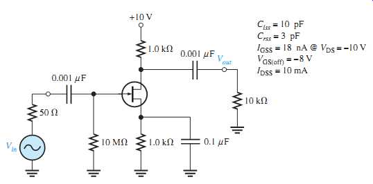
FIG. 57
Sect. 2 The Decibel
8. A certain amplifier exhibits an output power of 5 W with an input power of 0.5 W. What is the power gain in dB?
9. If the output voltage of an amplifier is 1.2 V rms and its voltage gain is 50, what is the rms input voltage? What is the gain in dB?
10. The midrange voltage gain of a certain amplifier is 65. At a certain frequency beyond midrange, the gain drops to 25. What is the gain reduction in dB?
11. What are the dBm values corresponding to the following power values?
(a) 2 mW (b) 1 mW (c) 4 mW (d) 0.25 mW
12. Express the midrange voltage gain of the amplifier in FIG. 56 in decibels. Also express the voltage gain in dB for the critical frequencies.
Sect. 3 Low-Frequency Amplifier Response
13. Determine the critical frequencies of each RC circuit in FIG. 58.
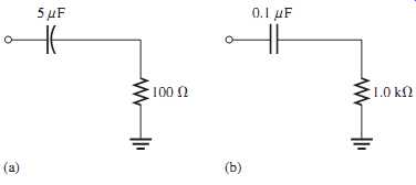
FIG. 58
14. Determine the critical frequencies associated with the low-frequency response of the BJT amplifier in FIG. 59. Which is the dominant critical frequency? Sketch the Bode plot.
15. Determine the voltage gain of the amplifier in FIG. 59 at one-tenth of the dominant critical frequency, at the dominant critical frequency, and at ten times the dominant critical frequency for the low-frequency response.
16. Determine the phase shift at each of the frequencies used in Problem 15.
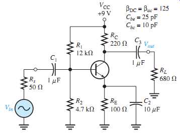
FIG. 59
17. Determine the critical frequencies associated with the low-frequency response of the FET amplifier in FIG. 60. Indicate the dominant critical frequency and draw the Bode plot.
18. Find the voltage gain of the amplifier in FIG. 60 at the following frequencies: fc, 0.1fc, and 10fc, where fc is the dominant critical frequency.
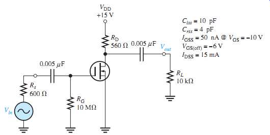
FIG. 60
Sect. 4 High-Frequency Amplifier Response
19. Determine the critical frequencies associated with the high-frequency response of the amplifier in FIG. 59. Identify the dominant critical frequency and sketch the Bode plot.
20. Determine the voltage gain of the amplifier in FIG. 59 at the following frequencies: 0.1fc, fc, 10fc, and 100fc, where fc is the dominant critical frequency in the high-frequency response.
21. The datasheet for the FET in FIG. 60 gives Crss = 4 pF and Ciss = 10 pF. Determine the critical frequencies associated with the high-frequency response of the amplifier, and indicate the dominant frequency.
22. Determine the voltage gain in dB and the phase shift at each of the following multiples of the dominant critical frequency in FIG. 60 for the high-frequency response: 0.1fc, fc,10fc, and 100fc.
Sect. 5 Total Amplifier Frequency Response
23. A particular amplifier has the following low critical frequencies: 25 Hz, 42 Hz, and 136 Hz. It also has high critical frequencies of 8 kHz and 20 kHz. Determine the upper and lower critical frequencies.
24. Determine the bandwidth of the amplifier in FIG. 59.
25. fT = 200 MHz is taken from the datasheet of a transistor used in a certain amplifier. If the midrange gain is determined to be 38 and if fcl is low enough to be neglected compared to fcu, what bandwidth would you expect? What value of fcu would you expect?
26. If the midrange gain of a given amplifier is 50 dB and therefore 47 dB at fcu, how much gain is there at 2fcu? At 4fcu? At 10fcu?
Sect. 6 Frequency Response of Multistage Amplifiers
27. In a certain two-stage amplifier, the first stage has critical frequencies of 230 Hz and 1.2 MHz.
The second stage has critical frequencies of 195 Hz and 2 MHz. What are the dominant critical frequencies?
28. What is the bandwidth of the two-stage amplifier in Problem 27?
29. Determine the bandwidth of a two-stage amplifier in which each stage has a lower critical frequency of 400 Hz and an upper critical frequency of 800 kHz.
30. What is the dominant lower critical frequency of a three-stage amplifier in which fcl = 50 Hz for each stage.
31. In a certain two-stage amplifier, the lower critical frequencies are fcl(1) = 125 Hz and fcl(2) = 125 Hz, and the upper critical frequencies are fcu(1) = 3 MHz and fcu(2) = 2.5 MHz. Determine the bandwidth.
Sect. 7 Frequency Response Measurements
32. In a step-response test of a certain amplifier, tr = 20 ns and tf = 1 ms. Determine fcl and fcu.
33. Suppose you are measuring the frequency response of an amplifier with a signal source and an oscilloscope. Assume that the signal level and frequency are set such that the oscilloscope indicates an output voltage level of 5 V rms in the midrange of the amplifier's response. If you wish to determine the upper critical frequency, indicate what you would do and what scope indication you would look for.
34. Determine the approximate bandwidth of an amplifier from the indicated results of the step response test in FIG. 61.
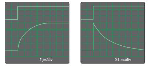
FIG. 61
APPLICATION PROBLEMS
35. Determine the dominant lower critical frequency for the amplifier in FIG. 52 if the coupling capacitors are changed to 1 uF. Assume RL = 29 kOhm and Beta_ac = 100.
36. Does the change in Problem 35 significantly affect the overall bandwidth?
37. How does a change from 29 kOhm to 100 kOhm in load resistance on the final output of the amplifier in FIG. 52 affect the dominant lower critical frequency?
38. If the transistors in the modified preamp in the Application Activity have a Beta_ac of 300, deter mine the effect on the dominant lower critical frequency.
DATASHEET PROBLEMS
39. Referring to the partial datasheet for a 2N3904 in FIG. 62, determine the total input capacitance for an amplifier if the voltage gain is 25.
40. A certain amplifier uses a 2N3904 and has a midrange voltage gain of 50. Referring to the partial datasheet in FIG. 62, determine its minimum bandwidth.
41. The datasheet for a 2N4351 MOSFET specifies the maximum values of internal capacitances as follows: Ciss = 5 pF, Crss = 1.3 pF, and Cd(sub) = 5 pF. Determine Cgd, Cgs, and Cds.
ADVANCED PROBLEMS
42. Two single-stage capacitively coupled amplifiers like the one in FIG. 56 are connected as a two-stage amplifier (RL is removed from the first stage). Determine whether or not this con figuration will operate as a linear amplifier with an input voltage of 10 mV rms. If not, modify the design to achieve maximum gain without distortion.
43. Two stages of the amplifier in FIG. 60 are connected in cascade. Determine the overall bandwidth.
44. Redesign the amplifier in FIG. 52 for an adjustable voltage gain of 50 to 500 and a lower critical frequency of 1 kHz.
FIG. 62 Partial datasheet for the 2N3904. Fairchild Semiconductor Corporation.