AMAZON multi-meters discounts AMAZON oscilloscope discounts
Introduction
Many applications of electronic circuits will require some adjustment to the frequency response of the system to produce an increase or a decrease in its gain at some part of its pass band in respect to another. This could entail either a gradual change in gain, as a function of input frequency, to lessen the magnitude of some signals with respect to others, or a more abrupt alteration in gain, perhaps to select some particular signal, or to cause the complete exclusion of other signals occurring at different parts of the input frequency spectrum.
Where the change in gain exceeds 6dB/octave (in which the gain is either halved or doubled by a halving or doubling of the input frequency), the generic term filter is usually employed, and such filters can be designed to operate either in low-pass, high-pass, notch, tuned response or bandpass arrangements. These filter systems can be built either in passive forms, using capacitors (impedance decreases as a function of frequency) or inductors (impedance increases as a function of frequency) in combination with resistors, or with each other, or as active layouts where the characteristics of the circuit are dependent on the effect of some form of feedback, either positive or negative, within the system. The term active is used to distinguish these circuit types from those where any gain blocks simply provide signal amplification, with out altering the effect of any LR, CR or LCR networks which are present in the signal path.
Active circuit designs arc preferable, generally, for high attenuation rate filters in low frequency applications, where large values of inductance would be needed to achieve the same result by passive LC systems. Such large inductors could also pose problems due to hum pick-up. For RF applications, above, say, 100kHz, passive LCR networks, often quite complex in design, are almost always employed. (See Section 11.) For convenience, I have divided the text into passive and active portions, in order to examine the various functions possible with both of these systems.
Passive circuit layouts
Low-pass circuitry
The simplest circuit arrangements used for this purpose are just RC or LR combinations of the kind shown in FIGs 1a, or 1b, which will give gain vs. frequency response curves of the kind shown in FIG2a, with a turn-over frequency, f_t (that frequency at which the gain has fallen by -3dB with respect to its value at frequencies well below the turn-over point), given by the equation:
…and an ultimate attenuation slope of-6dB/octave. The LCR circuits shown in FIGs 1c and 1d, give a hump in the frequency response curve at the turnover frequency, but because they include two reactive components, will give an ultimate attenuation rate of -12dB/octave, as shown in FIG2b. The turnover frequency is given approximately by the equation:
…though the actual value of f_t is modified a little by the presence of Rc.
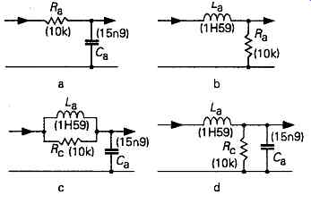
FIG1 RC, LR and LCR low-pass filter layouts (ft = 1000 Hz).
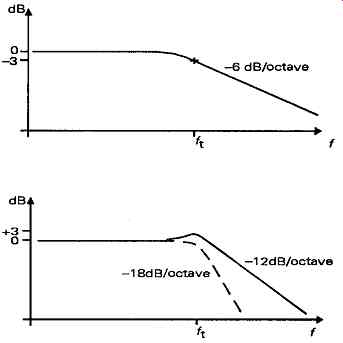
FIG2 Frequency response curves for circuits of FIG1.
In most practical applications, it’s necessary for La or Ca to be shunted by a resistance, Rc, having a value similar to that of the impedance, at ft , of either the inductor or the capacitor, in order to prevent the circuit presenting the signal source with a near-zero load impedance at the series resonant frequency of the LC circuit, and to limit the size of the hump in the frequency response. However, the presence of this hump, even when damped by V? c , does allow the interesting possibility that the circuit of FIG1c could be folio wed by a simple RC attenuator circuit, such as that of FIG1a, to give the layout shown in FIG3, which will, if the component values are chosen correctly, both level out the hump and give an attenuation slope of -18dB/oclave, as shown by the dashed line in FIG2b.
FIG3 Filter circuit for -18 dB/octave slope
In deciding what component values should be employed for these types of circuit, it’s sensible to consider at what overall impedance level one wishes to operate, and then choose values of f, and C or L, whose impedance at f_L is near to the required circuit impedance level.
It’s customary, in considering the performance of all the frequency response modifying systems described in this section, to assume that they are driven by a signal source having a very low output impedance, and that they will feed a load which has a very high input impedance. If this is not the case, simple opamp, buffer stages, of the kind shown in FIG4a, could be interposed between the filter circuit and its source or load to satisfy this requirement. Similar frequency response characteristics are given by the shunt and series feedback layouts shown in FIGs 4b and 4c, for similar values of Ra and Ca, though, in this case, there will be some gain in signal level determined by the ratios of Ra to Rb. In both of these circuits, Ra, or some equivalent DC path, is essential in order to provide a DC negative feedback path to stabilize the working point of the gain block.
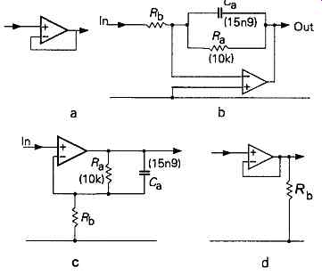
FIG4
It should be remembered that, as mentioned in Section 7, there is a small residual difference in the frequency response of these two circuits, since, apart from the additional circuit gain, the frequency response curves of the circuits of FIGs 1a and 4b are substantially identical, giving a stage gain which will fall to zero at very high frequencies.
By contrast with this, the circuit of FIG. 4c gives a gain which decreases only to unity, because when the frequency is high enough for the impedance of Ca to be negligibly small, the circuit effectively becomes equivalent to that of FIG. 4d, which is a simple unity gain buffer stage. This gives a frequency response of the kind shown in FIG5, which is equivalent to that of the passive circuit of FIG. 6.
The series feedback circuit layout of FIG. 4c has the significant advantage that it offers a very high input impedance, which means that the source impedance does not need to be low, and it’s therefore used more often in practical circuit layouts.
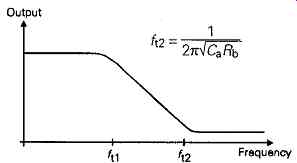
FIG. 5 Frequency response of circuit of FIG. 4c
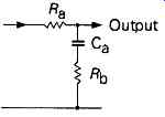
FIG. 6
Although simple, single CR, networks are often used, for example in the two audio tone control net works shown in FIGs 7a and 7b, which give the type of frequency response curves shown in FIG7c, more complex combinations of capacitors and resistors are often used, either as a simple network, or in the negative feedback path of a gain block, as shown in FIGs 8 and 9, which are typical RIAA equalized gramophone record replay, and 'NAB' equalized cassette tape head replay amplifier arrangements, for which the frequency response curves are shown in FIGs 10a and 10b.
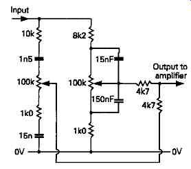
FIG. 7a Typical passive tone control circuit.
FIG. 7b Baxandall type negative feedback tone control circuit.
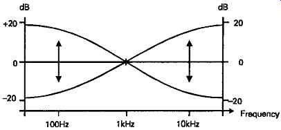
FIG. 7c Frequency response curves of tone control circuits.
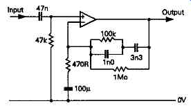
FIG. 8 Typical R!AA compensation pick-up input stage.
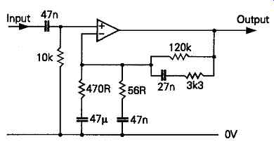
FIG. 9 Tape recorder (3.5 cm/sec) replay equalization circuit.
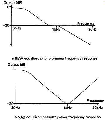
FIG10 . a RIAA equalized phono preamp frequency response
High pass circuitry
Circuits of this type are simple rearrangements of FIGs 1- 3, with the positions of some capacitors, inductors and resistors interchanged, as shown in FIGs 11-12. The frequency response characteristics of the circuits of FIGs 11 are shown in FIGs 13a and 13b/c, in which the turn-over frequency is given by the same equations quoted above. These circuits can also be connected around opamp gain blocks as shown in FIGs 14 and 15, to give output characteristics which will rise with frequency, as shown in FIG16. In the absence of Rc, the gain would increase continuously, as the frequency increased, up to the open-loop gain of the amplifying stage. With Rc, there will be two turn- over points, an LF one whose +3dB point will be given by ...
…and a higher frequency one, at which the gain will again level off, whose turn-over point is given by…
Notch filters
This kind of response characteristic, which is used to remove a specific single frequency from the pass-band of the circuit, can be provided by a variety of circuits, of which the two most common are the parallel resonant LC filter, and the parallel-T circuits shown in FIGs 17 and 18, for which the notch frequencies are given by …respectively.
If low loss capacitors and high 'Q' coils (i.e. those with low internal resistive losses), are used in the circuit of FIG17, and if the source resistance is low, and if the load resistance, RL, is chosen so that its value is high in relation to the AC impedance of the inductor, but low in relation to leakage impedances, quite a good ultimate attenuation factor, coupled with sharp notch can be obtained.
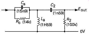
FIG11 Rearrangements of circuits of FIG1 as high-pass layouts (ft = 1000
Hz for values shown)
FIG12 Third-order (-18dB / octave) high-pass LCR filter
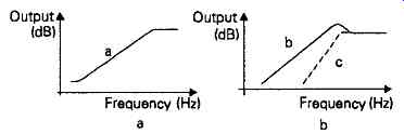
FIG13
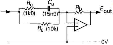
FIG14
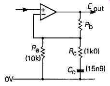
FIG15
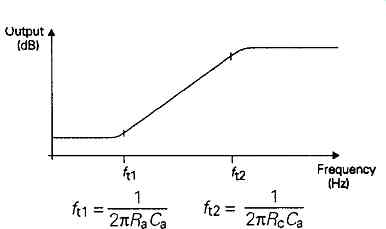
FIG16
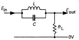
FIG17 Simple LC notch filter
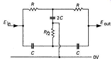
FIG18
The notch frequency attenuation given by the circuit of FIG18 can be extremely high, if precise value components are used, though the steepness of the cut-off slope, on either side of the notch, is not very good, as illustrated by the solid line curve in FIG19. Negative feedback can be used to sharpen up the notch, with the circuit arrangement shown in FIG20, which gives the type of response shown in the dashed curve in FIG19. The sharpness of the notch, in this case, can be adjusted by the setting of Output 4.
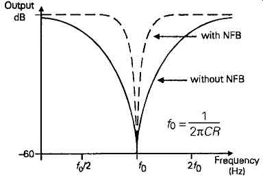
FIG19 Frequency response of parallel-T notch filter (LF351)
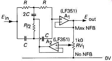
FIG20 Way of applying negative feedback around parallel-T filter circuit
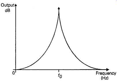
FIG21 Frequency characteristics of LC tuned response filter
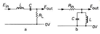
FIG22 LC tuned response filter circuits
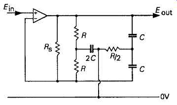
FIG23 Tuned response filter based on bridged parallel-T circuit
Tuned response
This kind of circuit is the opposite of the notch filter, in that it can be used to select one particular frequency from an input spectrum of signals, with the kind of frequency response shown in FIG21. The LC circuits shown in FIGs 22a and 22b can do this, provided that the values of R-m and the load resistor, RL are chosen appropriately, with the limitations noted earlier about the bulk -- and likely low Q -- of large values of inductor necessary for use at low frequencies, together with their susceptibility to hum pick-up.
An alternative approach is to insert a parallel-T notch filter in the feedback path of a gain block, as shown in FIG23, but this must be by-passed by a gain limiting resistor, Rs, or the circuit will oscillate continuously.
Bandpass circuitry
In principle, this is merely a high-pass circuit, followed by a low-pass one, such as shown in FIGs 24, which will give the type of response shown in FIG25, where the separation between the two turn-over frequencies, f_t1 and f_t2, can be adjusted to give the appropriate pass-band. However, in practice, R2 and C2 will need to be high in value compared with R1 and C1 to get a reasonable degree of independence in the operation of the two halves of the circuit. This layout, and the frequently recommended opamp system shown in FIG26, of which the performance is shown in FIG27, don’t really give a high enough frequency discrimination to be of much use in practice, and active circuit layouts giving higher 'skirt' attenuation rates are generally preferred. For RF applications, this need can be met very satisfactorily by the coupled tuned circuit layout shown in FIG28.
The operation of this kind of circuit is examined in greater detail in Section 14.
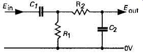
FIG24 Simple cascaded RC bandpass filter
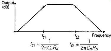
FIG25 Frequency response of circuit of FIG24
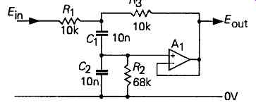
FIG26
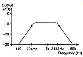
FIG27 Frequency response of circuit of FIG26
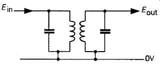
FIG28 Bandpass-coupled tuned circuits
Active filter circuitry
Introduction
As a general rule, this term is used to describe systems which contain amplifying or impedance converting elements, capable of injecting energy into the system, and which can be used to modify the characteristics of the passive components, Cs, Rs and Ls, which are used in the circuitry.
A point which should be remembered in connection with such circuits is that, because of the energy injected by the active component, it’s possible for them cross over the borderline between stable operation and continuous oscillation, if the operating conditions are incorrect -- as, perhaps, might lie the case of an active filter whose input becomes open-circuited.
I have lumped the two main categories of active filter together since these can often be interchanged in their mode of operation, from high-pass to low-pass and vice versa, by simply interchanging the positions of the appropriate Cs and Rs. There are a few exceptions, which will mainly concern those circuits where a simple transposition would make the DC bias paths awkward to implement, or where the intrinsic HF gain or phase characteristics of the gain block will influence the final result.
High-pass (HP) and low-pass (LP) filters
A simple example of the way a gain block can be made to increase the rate of attenuation in the gain/frequency characteristics of a circuit, above or below some specific turn-over frequencies -- by the use of negative feedback, applied around the amplifying block -- is shown in FIG29. Without NFB, the gain of the system, as a function of frequency, shown in the dashed line of FIG30, is very non-uniform. If, however, NFB is applied, the response of the system is modified, as shown by the solid line curve in FIG30. This shows not only that the gain is more uniform a function of frequency, though at a lower gain level, but also that the LF and HF frequency response is extended beyond the open-loop turnover points.
Moreover, beyond these points, and this is the feature of particular interest, it can be seen that the application of NFB causes the response to fall at a much steeper rate than would have been the case without it. This suggests an approach by which a simple low-pass active filter could be made. If an amplifying block, such as the opamp shown in FIG31a, is preceded by an input RC circuit, R2/C{ < so that, left to itself, the system would have a falling gain with in creasing frequency, and negative feedback is then applied, via R3, to the junction of R1 and R2, then the circuit will give the type of frequency response shown in FIG32, as the NFB operates to maintain a constant gain for all input frequencies.
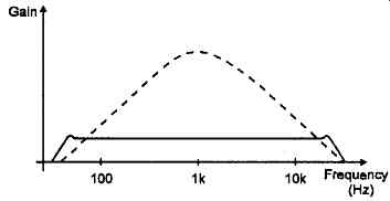
FIG. 30 Effect of NFB on frequency response of gain block
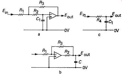
FIG. 31 Method of constructing an active low pass filter
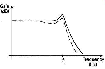
FIG. 32: Gain + (dB) ft Frequency (Hz)
The circuit layout shown in FIG31b would be inappropriate for this purpose because, as shown in Section 7, the loop feedback would have the effect of reducing the output impedance of the opamp. (which, in effect, will be largely that due to R2,) by the factor (1 +/4B), where A is the open-loop amplifier gain, and B is the feedback factor, giving an effective output impedance value of R2/(i + AB). C1 would therefore need to be very much larger in value than a simple f_t calculation based on RJCX would suggest, and it would also mean that, while the HF gain would indeed fall quite steeply beyond some turn-over point, this would mainly be due to the limited ability of the opamp. at higher frequencies, to drive current into C1 which would result in fairly severe distortion of the output waveform.
In both of the circuits of FIG. 31, there would be a prominent peak in the frequency response at the point preceding the fall in gain. This is because, in all normal opamps, as a result of their internal HF compensation components, there is an internal input/output phase shift of 90°, which, when added to the phase shift due to R2/C1, will cause the overall feedback to cease to be negative in character, and approach the condition of positive feedback. This will always increase the stage gain, and can, in some circumstances, lead to continuous oscillation.
If an additional RC HF attenuation network is added to the circuit, as shown in FIG. 31c, the size of this hump in the frequency response can be reduced, and this RC network will also cause the rate of HF attenuation to be increased, as shown in the dashed line in FIG. 32. The penalty is that, in order for the added RC network to do much about removing the hump in the curve, it will also cause some loss of gain at frequencies below the turn-over point, which will usually be undesirable. This brings up the point of the flatness of the frequency response of a filter, in relation to the ultimate rate of attenuation of the system, be tween which there must usually be some compromise, since the circuit considerations which improve the one will usually impair the other.
A further consideration in all filter types is the time delay which they will introduce: a factor which also tends to impose constraints on the filter type chosen.
This implies that some choice must be made, in most cases, between the various options, and has led to the specification of filter characteristics as 'Butterworth', in which flatness of frequency response within the pass-band (i.e. below or above the turn-over point, in the case of LP and HP filter types) is optimized at the expense of ultimate attenuation rate.
The second option, that in which the attenuation rate is maximized at the expense of pass-band flatness, is known as the 'Chebyshev' type of response, and a variation of this, in which flatness of frequency response, even outside the pass-band, is sacrificed for steepness of cut-off characteristics, is known as the 'Cauer' response. The final common filter form is the 'Besser, which is the type of design in which the layout is chosen to minimize time delay. The general transmission characteristics of these filter types, in comparison with a simple RC network, are shown in FIG. 33.