AMAZON multi-meters discounts AMAZON oscilloscope discounts
Introduction
'Feedback' is the term which is given to the introduction of a signal voltage, derived from the output of what is usually an amplifying stage, into the input of that stage. This feedback can be present as a deliberate feature of the circuit design, but may also occur inadvertently, either because of shortcomings in the amplifying devices or other circuit components which are used, or because of oversights in the design of the circuitry in which they are employed. Whatever the cause, the presence of feedback can significantly alter the performance of the circuit, so, although this can be a rather complex aspect of circuit theory, it’s necessary for its effects to be broadly understood by any engineer seeking to try his hand at circuit design.
The basic effects of feedback
If the polarity of the signal which is fed back is of the same sign as that input signal which generated it, then the feedback signal is said to be 'positive'. If its polarity is opposite to that of the input signal, it’s said to be 'negative'. (Because negative feedback is such a common feature of circuit design, it’s often just referred to as NFB).
In the case of positive feedback (which I shall call PFB), because the signal which is fed back is of the same polarity as the input signal, it will act to increase the size of this signal, which will, of course, then increase the size of the output signal, which will, in turn, increase the size of the voltage which is fed back.
Clearly, unless there is some loss of signal somewhere in the system, or some constraint on the possible input or output voltage swing, this process would cause the gain block to produce an infinitely large output. In a DC system, this effect will usually cause the system to 'latch up' -- a condition in which the output voltage is driven fully towards one or other of the voltage limits of which the output is capable. In an AC coupled system, the result will usually be a continuous and uncontrolled oscillation. Both of these effects of PFB can be utilized in circuit design.
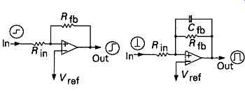
FIG1 The use of positive feedback to provide bistable or mono-stable logic
elements.
For example, in the DC systems shown in FIG1, the circuit layout can be arranged to provide either a 'bi-stable' or a 'mono-stable' function block. In the first of these forms, shown in FIG1a, the output voltage can be made to jump rapidly from one stable output voltage state to another, where it will rest until a suitable input signal restores the original output voltage condition of the circuit. In the second case, shown in FIG1b, the output voltage can be made to change from its normal rest condition to a different voltage level, where it will remain for a period of time, determined in this case by the values chosen for Cfb and f ?fb, before reverting to its original state. Both of these types of function are widely used in logic elements.
Positive feedback, in an AC circuit, can be used to produce a continuous oscillatory voltage output, which could be used as a signal source, although for this purpose some means of controlling both the frequency of oscillation and the amount of feedback -- which will determine the output signal voltage -- is necessary. As an example of this, in the simple 'Wien bridge' oscillator circuit, shown in FIG2, the system is made to oscillate continuously by the use of positive feedback, which is applied from the output to the non-inverting input of a gain block (Ai), via the RC Wien network -- R\Cu RlCi -- (in which R1= R2, and C1=C2). This network has the interesting characteristic that, at a frequency at which the impedance of R2+C2 is twice that of R1 in parallel with C\ (for which the shorthand notation R\\\C\ is often used), the out put, at point ?\ is in phase with the input, at point ? \ and if the gain of the amplifier is equal to, or slightly exceeds 3, the circuit will give a sinusoidal output signal at a frequency defined by the equation:
F=1/(2 pi CR).
In practical oscillator circuit designs of this type, negative feedback, by way of a signal applied to the inverting input of the gain block, is then used to control the gain of the amplifier, so that is high enough to cause the circuit to oscillate, but not so high that the output sinewave signal is distorted by 'clipping', due to the limits on the output voltage swing imposed by the supply voltage rails. This can be done quite conveniently, by the use of an output voltage-dependent component, such as the low-power thermistor (TH1), shown in FIG2, whose resistance value decreases as the output voltage increases, and which will thereby control the amount of the negative feedback signal applied to the inverting input of the gain block. If the value of 7?f b is chosen correctly, this NFB input will reduce the gain so that it’s exactly equal to 3 at the desired AC output voltage swing.
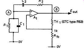
FIG2 A 'Wien bridge' oscillator using both +ve and -ve feedback.
It’s convenient, for the purposes of explanation of circuit behavior, to postulate an ideal amplifying gain block, having inverting (-in) and non-inverting (+in) inputs, an infinitely high value of internal gain, and a zero impedance output point, a concept which is called an 'operational amplifier'. Devices such as the integrated circuit wide band gain blocks, such as the '741' type device, and particularly the later and improved FET input versions of this kind of circuit, such as an 'LF351' or the TL051' come very close to satisfying the operational amplifier specification, in that they have a very high gain (100,000 or greater), a low output impedance (less than 200 ohms), and, especially in the case of the FET-input versions, very high input impedance, and are indeed described as opamps.' in the makers' catalogs.
If an IC of this kind is used as the gain block, shown symbolically as Ai in FIG2, operated from +/ 15V supply rails, the output voltage swing is set, by the choice of Rfb, to lie between 1V and 3V RMS, the total harmonic distortion of the circuit would be of the order of 0.01-0.03%, at 1kHz.
In the notation used in FIG3 (and which I have also used in FIGs 1 and.2), the symbols '+' and '-' within the triangular opamp. diagram, are taken to represent the 'non-inverting' and 'inverting' inputs of the amplifier. The + and -- symbols outside the triangle are taken to represent connections to some external DC power supply (typically +/-15 V), though these connections are often omitted from the circuit diagram unless their connections are, in some way, significant in respect of the operation of the circuit.
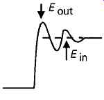
FIG3 Conventional notation for 'operational amplifier' type of gain block
Positive feedback can also be used, with care, to increase the AC voltage gain, or output swing obtain able from an amplifier circuit. A very common example of this is the use of a 'bootstrapped' load resistor, as in the circuit of FIG4 (the term is said to derive from the fanciful idea of lifting oneself up by ones own bootstraps'), which is commonly used to increase the effectiveness of the driver stage in simple audio amplifier designs. In this circuit, a volt age signal derived from the outputs of the two push pull emitter-followers (Q2/Q3) (point R), is coupled back to the +ve end of RA (point S), by way of O, so that if the output voltage at R, swings up or down, the potential at point S will follow this voltage excursion.
This greatly increases the stage gain due to Q1, by virtue of the positive feedback signal, because it makes the dynamic impedance of RA much higher than its static value. However, except in circuit layouts which are deliberately designed to function as 'free running' oscillators -- a topic which is explored at greater length in Sections 10 and 13 -- positive feedback is generally avoided, and precautions are frequently taken to avoid its inadvertent occurrence, since it can lead to undesirable effects on the circuit performance.
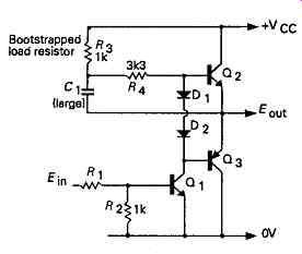
FIG4 The use of a bootstrapped load resistor (R3) to increase available
output voltage swing
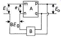
FIG5 Schematic gain block with feedback loop
The effect of feedback on gain
The basic characteristics of a simple series feedback circuit (i.e. one in which the feedback signal is applied in series with the input signal) can be explained by reference to the block diagram shown in FIG5, in which the square symbol is used to represent a circuit element with a gain of A, and which has two independent and isolated input and output circuits, m -- n and p -- q, arranged so that an input signal voltage e, applied between m and n will generate an output voltage of Ae between p and q, without sign inversion.
If we define the signal actually applied between the input points m and n as e\% and the signal appearing at the output points p and q as £0, then the stage gain of the amplifying block, A, is:
D A=^ which is known as the 'open-loop' gain -- i.e. the gain before any feedback is applied.
However, if there is an electrical network between the output and the input of this gain block which causes a proportion ß of the output signal to be returned to the input circuit, in series with the applied input signal Eu then the actual input signal fed to the gain block will be altered so that e\ will actually be E\ + ߣ0, or …
From these equations, we can determine the effect of feedback on the stage gain, bearing in mind that, in the absence of a feedback signal, E\ = e\. The closed-loop stage gain, i.e. that when feedback is applied, I have called A', and is defined by the equation …
There are several conventions for the names used in feedback systems, but the one I prefer is that in which the term 'ß?', the product of the 'open-loop' gain and the proportion of the signal reintroduced to the input by the feedback network, is referred to as the "feed back factor".
It must be remembered that, in this equation, the sign of ß may be either positive or negative depending on the configuration of the feedback network. In the case of a NFB system, ß is negative, so that the gain becomes A/(l + ß?)
[A confusing usage of the term feedback factor, which I think should be avoided, is when it’s employed, in NFB systems, to describe the amount of negative feedback used in the design. This is usually expressed in dBs, and is normally defined as the extent to which the open-loop gain is reduced when negative feedback is applied {i.e. A'/A or 1/(1 + ß?)}. For example, if the closed-loop gain of an amplifier, with NFB, was reduced to one hundredth of its open-loop value, (-40dB), this would be described as 40dB of negative feedback.]
Considering the relationships shown in equation (4), in the particular case where the network is non-inverting, and the feedback signal is returned to the input in the same phase (positive feedback), so that {A'/A = 1/(1- ß?)}, the situation arises in which the larger the feedback factor Aß, becomes, the smaller the denominator in this equation will be, and the higher the effective gain of the system -- up to the point where Aß = 1, when the denominator in the equation would become zero, and the closed-loop gain, A, would become infinite. This is the condition which will lead to 'latch-up' in a DC coupled circuit, or continuous oscillation in an AC coupled one, as, for example, in the Wien network oscillator described above, which will oscillate when E0 = 3Ei, and ß = 1/3, which leads to the condition that ߣ0 = E\.
If the feedback network is a phase inverting one, so that ß is negative, the gain equation will become ...
In this case, the closed-loop gain will decrease as the amount of feedback is increased, up to the point at which ßA is so much greater than 1 that the equation approximates to ...
This is particularly appropriate to those cases in which the open-loop gain (i.e. the gain before the application of feedback) is very high; as would nearly always be the case with operational amplifier integrated circuits at low to medium signal frequencies. In these circum stances, the gain is determined almost entirely by the attenuation ratio of the feedback network, so that if ß is 1/10, then the gain will be 10, and if ß is 1/100, then the circuit gain will be 100.
This is a very useful effect, in that it makes the gain of the circuit arrangement almost completely independent of the gain of the amplifier block itself, so long as this is high in relation to ß. A specific advantage which arises in this case is that, if the feedback net work has an attenuation ratio which is constant, and independent of frequency, then, so long as the gain of the amplifier block remains high in relation to ß, then the system will have a stage gain of 1/ß and this will also be independent of operating frequency.
The use of NFB to reduce distortion
In addition to the improvement which NFB can make to the flatness of the frequency response of an amplifier, it will also, within limits, reduce harmonic and waveform distortion, as well as any 'hum' and noise generated within the amplifying circuit, which can indeed be considered as just another aspect of signal distortion.
If the instantaneous relationship, between the input signal applied to a circuit block and the output voltage from that block, is considered to be its amplification factor, then any 'distortion' in the output signal can be regarded simply as an indication that the effective amplification factor of the system has changed during the transmission of the signal. This change might be the result of a variation in output voltage with time, within the duration of a nominally constant signal, perhaps because of the intrusion of mains hum or noise. Alternatively, it could be due to the characteristics of the system itself -- as shown in the case of the square-wave signal illustrated in FIG6. Again, it could be an unwanted change in the signal wave form, in the case of a continuously varying input signal voltage, because the gain of the system is influenced by the instantaneous magnitude of the input signal, due to nonlinearity in the input/output transfer characteristic, shown in FIG7.
FIG6 Distortion of step-waveform due to circuit characteristics
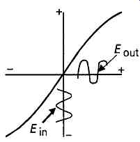
FIG7 Distortion due to nonlinear amplifier transfer function
However, if the amplifier gain, A, is sufficiently high that the closed-loop gain (AO, becomes simply 1/ß, and if the factors which determine the value of ß are themselves noise and hum free and distortionless, then the output signal must also be distortionless, noise and hum free, simply because variations in the open-loop amplifier gain A, as a function of input voltage or time, are no longer factors which influence the output volt age. This is only strictly true for infinitely high values of A, but even for lower values of A the distortion will still be reduced by the feedback factor (1 + ß?), as shown by the following analysis, due to Langford Smith (Radio Designers Handbook, 4th Edition, Section 7).
Let a sinusoidal input voltage, E1, of an amplifier employing negative feedback be defined by the term E'un cos ??, where ? = Inf. Then, if the amplifier introduces harmonic distortion, the output will be …where w om, w 2m and w 3m are the peak values, respectively, of the fundamental, second and third harmonic frequencies, etc. The feedback voltage (ß w 0) will therefore be …
The voltage applied to the input of the amplifier will be …
Since E0 = Aeu the output voltage will therefore be …where Ho and H3 are the ratios of the second and third harmonic voltages to the voltage of the fundamental in the amplifier without feedback.
But the output voltage has already been defined by equation (6), so, by equating the fundamental components of equations (6) and (7)
Equating the second harmonic components in equations (6) and (7) ...
Inserting the value of e_im from (8)…
Therefore, <?2m( 1+ ßA) = EomH2 and, by the same argument, e3m/E0m = #3/(1 + ß?), and so on, for any higher order harmonics. That is to say that, so long as the feedback is negative, so that the term in the denominator is 1 + ß?, the magnitudes of all the harmonics, and the consequent intermodulation products, caused by the nonlinearities in the amplifier, will be reduced by the same proportion by which the gain is reduced (see equation (3)). However, this conclusion is only strictly accurate if the feedback is truly negative (i.e. 180° out of phase with the input signal), and if the gain of the amplifier is the same for the harmonic frequencies as it’s for the fundamental, and these conditions are unlikely to be met, precisely, in any real-life amplifying circuit. Nevertheless, this conclusion is broadly true.
A similar mathematical process can be used to show that hum and noise will also be reduced as the gain of the amplifying circuit is reduced, but it’s simpler, I think, to resort to the logical argument that, if the input signal itself is hum and noise free, then if the gain of the amplifier is reduced by feedback, and the magnitude of the input signal is raised so that the output remains constant, then the proportion of hum and noise in the output signal which was introduced by the amplifier will be reduced by the same amount.
Negative feedback will reduce the output impedance of an amplifier, when measured at the point from which the feedback path returns to the amplifier input, by (1 + ß?), and, in the case of a 'series feedback' circuit, it will also increase its input impedance, in comparison with the same amplifier without NFB, by the same factor. However, this effect on input and output impedances is also only true while the open loop gain of the amplifier remains high, and while the feedback remains negative.
At frequencies where the gain of the amplifier is low, and its internal phase errors cannot be ignored, the effects of feedback on its input and output impedances are much more difficult to predict.
Problems with negative feedback
As mentioned above, it’s unlikely that NFB in any real-life circuit will ever be truly 'negative'. This difficulty arises principally because the response of any amplifying -- or other -- circuit to a change in the input signal level can never be truly instantaneous. In the case of a simple DC circuit, this means that if it’s presented with a sudden change in its input signal level, as shown in FIG8a, there will be some small, but inevitable, time delay before there is a corresponding change in the output signal level, as shown by the solid line in the diagram.
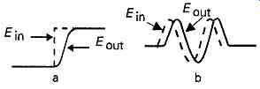
FIG8 The effect of circuit time delays on the output signal waveform
In an AC circuit, where the input potential is continuously varying, as shown in FIG8b, this same time delay within the system will result in an output signal which is shifted in phase -- a * phase lag' of the output waveform -- in relation to the input one. Clearly, the higher the frequency of the input signal, the greater the effective phase lag which will be caused by the same time delay -- or delays, where there are several contributing elements -- and the more complex the effect of the feedback signal will be. Depending on the nature of the circuit, this could well lead to the situation where a feedback voltage, derived from the output signal of an amplifying stage, was, in reality, positive (gain increasing and stability diminishing), whereas the designer of the circuit had intended it to be negative. If the feedback factor ß?, at the input frequency where this circumstance arose, became equal to unity, the circuit would become unstable and oscillate.
This incipient problem with amplifying circuits employing NFB was analyzed by H. Nyquist (Regeneration Theory, Bell System Technical Journal, Jan. 1932, p. 126), and H. W. Bode (Network Analysis and Feedback Amplifier Design, published by Van Nostrand, 1945), who both proposed graphical representations of the (closed-loop) gain and phase characteristics of the circuit.
In the case of the Nyquist plot, both of these effects are shown in a single diagram, by using the length and direction of a vector to indicate, respectively, the gain and phase shift of the system on a . single line graph, as shown in FIG9, where the angular orientation of the vector -- of which only its terminating point is usually shown in the drawing -- is used to indicate the measured phase shift at each value of operating frequency, and its length is used to define the closed-loop gain. If this vector graph encloses the point -1 and 180°, the system will be unstable.
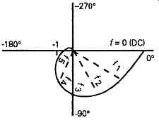
FIG9 The 'Nyquist' gain/frequency diagram
In the case of the Bode diagram, shown in FIG10, the open-loop gain of the system (A), and the phase shift of the feedback signal, are shown as two separate lines on the same diagram. In this case, how ever, an assessment as to whether the system meets the basic requirement for stability (that is to say that the open-loop gain shall be less than unity at the frequency at which the phase shift is 180°) and the determination of the system 'gain' and 'phase' margins, requires consideration of both the 'gain' and 'phase' graphs. If the gain is less than unity at the 180° phase shift frequency, but, at some other point, where the phase shift is greater than 180°, the gain exceeds unity, the circuit may not oscillate, but will be what is described as 'conditionally stable'. This is seldom a condition which is sought, although it can arise as a result of oversights or design shortcomings, and carries the risk that the system may subsequently become unstable if component characteristics change through aging.
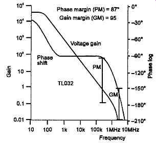
FIG10 'Bode diagram' illustrating gain and phase characteristics of commercial
'operational amplifier' IC.
'Stability margins' refer either to the extent to which, in a stable system, the gain would require to be increased at the 180° phase shift frequency for it to reach unity, a factor known as the gain margin, or to the extent to which the loop phase shift would need to be increased at the unity gain frequency, for it to reach 180°, which is known as the phase margin. Obviously, the higher the values of gain and phase margins which can be contrived within a closed-loop system the less likely it will be that changes in operating conditions or load characteristics will impair the stability of the circuit. This aspect of feedback design is particularly important in systems, such as audio amplifiers, where the characteristics of the load, such as, for example, a loudspeaker, will change greatly as a result of changes in operating frequency or drive level.
Unfortunately, in practical circuit design, it’s seldom possible to arrange for the provision of high levels of gain and phase margins without incurring some other design penalty, such as, perhaps, a higher order of residual harmonic distortion than could have been achieved with a less comprehensively stable system, so it’s useful for the would-be designer to understand the origins of phase shifts within circuit structures, and also the techniques by which these can be manipulated.
The relationship between frequency response and phase shift.
As a general rule, any circuit arrangement which gives rise to a change in gain from input to output as a function of frequency, will introduce a shift in phase, also as a function of frequency. Also, as a general rule, the greater the change in gain with frequency, the greater the effect it will have upon the phase shift, so that, for example, some circuit arrangement which causes a change in gain of 6dB/octave will have an associated ultimate phase shift of 90 degree, one causing a 12dB/octave change in gain will lead to a 180 phase shift, and so on.
Taking the case of the simple RC lag network, shown in FIG11a, and its associated Bode diagram, shown in FIG12, it will be seen that the phase lag, of voltage output with relation to the voltage input, begins at f_t/10, where f is the turn-over frequency -- defined as the frequency, f = 1/(27t RC), at which the gain had decreased by a factor of 0.708 (-3dB). Input rt; Output; Input L
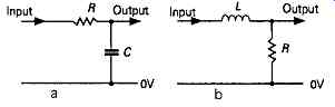
FIG11 Simple low-pass networks
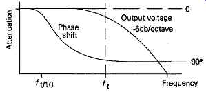
FIG12 Basic relationship between phase shift and frequency response
An exactly similar pair of gain/phase curves would be given by the simple LR network shown in FIG11b, or by any other arrangement which had the same effect.
Conversely, if the characteristics of the circuit are such that it has a transmission which decreases as the frequency is reduced, then there will be a phase shift due to this which will begin to appear at 10 ft, where, as before, f is the frequency at which the attenuation is -3dB. However, in this case, there will be a phase 'lead' rather than a phase lag, as shown in the gain/phase diagrams of FIG13, which would apply to either the simple RC network of FIG14a, or the L R network of FIG14b.
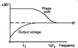
FIG13 Phase characteristics of high-pass network
FIG14 Simple high-pass networks
An inevitable consequence of the relationship be tween changes in transmission with frequency and associated phase shifts is that, for example, a transistor amplifying stage, of the kind shown schematically in FIG15, whose gain would inevitably decrease with increasing frequency beyond some HF turn-over point, would also introduce a phase shift, at ft/10, if ft was the -3dB point in its HF gain curve.
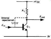
FIG15 Simple transistor amplifying stage
In practice, the gain/frequency behavior of even a simple transistor amplifying circuit would be much more complex than this, because, in addition to the time delays due to the charge carrier transit time within the device, there would be straightforward RC lag effects due to stray circuit and inter-electrode capacitances. This has the effect that if a string of, say, three transistors is connected as an amplifying circuit using negative feedback; as shown in FIG16, where, with ideal devices, the output, at HF, would be exactly in antiphase with the input; it’s improbable that it would be stable unless the feedback factor is very low, due to the accumulated incidental phase shifts within the circuit, mainly due to the transistors.
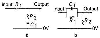
FIG16 Three-stage transistor amplifier
A possible, though crude, method for making such a circuit stable, at HF, would be to connect a relatively large value of capacitor, C1, across the collector load resistor of one of the transistors in the circuit, so that the gain had decreased to a sufficiently low value before the frequency was reached at which the incidental circuit and device phase shifts had become significant in their effects. This added capacitor would usually need to be large enough to reduce the HF turn-over point of the circuit to a frequency which would be, at the most, one tenth of that due to the fall-off in HF response due to the transistor circuit on its own.
Similarly, if phase shifts, due to coupling components, such as C1, Co and C3, occurred at the low frequency end of the circuit pass band, the application of closed-loop negative feedback would also lead to instability, and any simple form of LF phase compensation, to prevent continuous LF oscillation, would require a very severe curtailment of the LF response.
Again, this would not indicate good circuit design.
There are several design techniques which can be used to lessen the phase error in such a circuit, of which one of the simplest is the use of a 'step' network, of the kind shown in FIG17a, for which the Bode diagram is shown in FIG18. Here, the phase lag, due to the reduction in gain, with increasing frequency, caused by Rf Cf, is removed as the gain/frequency graph levels off , which gives rise to a phase lead (in reality, a decreasing phase lag) at a frequency deter mined by Ri/Cf.
FIG17 RC step networks for HF and LF phase error correction
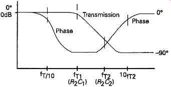
FIG18 Gain and phase characteristics of circuit of Figure 17a.
A similar step network, of the kind shown in FIG17b, can, of course, be used as a phase correction method at the LF end of the spectrum. In practice, with solid-state circuit design, it’s usually possible to arrange that the inter-stage DC potentials are such that it’s possible to omit inter-stage coupling capacitors, so that LF closed-loop instability does not occur. Unfortunately, though, the intrinsic characteristics of all amplifying devices lead to inconvenient phase shifts at the HF end of the system pass-band, and some form of HF compensation is usually essential to avoid closed-loop instability.
As an example of this, an HF step-network could be used to stabilize a feedback amplifier- whose gain and phase characteristics, shown in the curves a and b in FIG19, indicate that the amplifier would be un stable at unity gain with closed-loop feedback -- by changing these to the curves a' and b', which would indicate stable closed-loop operation.
A typical transistor operated gain block is shown in FIG20, in which transistors Q1 and Q3 are connected as an input long-tailed pair, Q2 and Q4 are constant current sources, and Q5 is the second stage amplifying transistor feeding the output emitter followers Q6 and Q7, for which a suitable forward volt age bias is provided by D3 and R5. If loop negative feedback is applied, by means of the external network Ra, Rb and Cb, the circuit will become unstable, and will oscillate at some relatively high frequency. It’s conventional practice to stabilize the circuit by the 'compensation' capacitor, C1, connected between the collector and base of Q5, which imposes a -6dB/octave fall in the amplifier frequency response, above some suitably chosen fc turn-over frequency. The effect of this capacitor, in this position, is greatly in creased by the voltage amplification of Q5, a phenomenon known as the Miller Effect. The reason why this happens is that if the input signal is such as to reduce the current through R1, which would cause the base voltage of Q5 to fall, the consequent rise in the collector voltage of Q5 will cause C1 to draw increased current through R1. This has the effect that the capacitance of C1 is multiplied by (1 + A), where A is the stage gain of Q5 in that particular circuit layout.
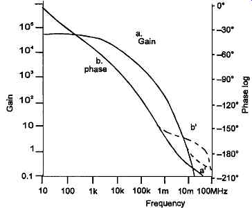
FIG19
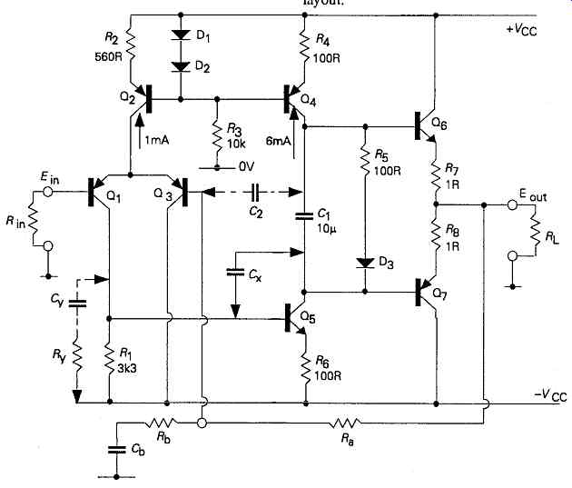
FIG20 Typical transistor gain block.
A practical snag inherent in this particular brute force method of closed-loop stabilization is that any sudden change of input signal voltage is likely to cause a temporary paralysis of the amplifier, while the capacitor C1 charges or discharges through Q1 or R1, a situation described as 'slew-rate' limiting. This causes the kind of response to a sudden voltage change which is shown in FIGs 21a and b. If some other signal is present at the same time as this sudden change of input voltage, it will be obliterated during the slewing period. This type of operational defect has been called 'transient intermodulation distortion'. This problem can be minimized if an input RC network is connected to the input of the amplifier, as shown in FIG22, to limit the possible rate-of-change of the input signal voltage.
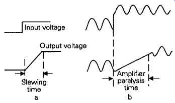
FIG21 Effect of compensation capacitor C1 on slewing rate and transient
intermodulation distortion
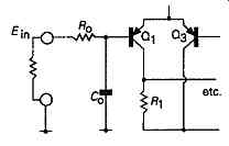
FIG22 Use of CR network to limit susceptibility of feedback amplifier to
slew rate limiting on input voltage step.
A better approach to the HF stabilization of the kind of gain block shown in FIG20 would be to connect a 'step' network, Cy/ Ry, across R1, in the collector circuit of Q1 . Alternatively, one could take advantage of the fact that the internal phase lag in the amplifier, between the base of Q3 and the collector of Q5, is not sufficient to cause instability if a capacitor, C_, is connected directly between these points. Such a capacitor can also be used to impose a -6dB fall in the HF response of the gain block, and ensure that the overall gain and phase margins are adequate to provide stable closed-loop operation, but without incurring the penalty of slew-rate limitation.