AMAZON multi-meters discounts AMAZON oscilloscope discounts
Introduction
Although it’s quite feasible to use thermionic valves for many of the applications where electronic signal amplification is required, it is, in general, very much simpler, and easier, and more cost-effective, to design using one or other of the available range of semiconductor devices, and I propose, therefore, to confine this section to 'solid-state' amplifying systems. However, for those who are interested in thermionic valve amplifiers, a few representative valve circuit designs are shown in Section 9.
The basic types of discrete solid-state device which are currently available to the linear circuit designer are bipolar junction transistors, in both NPN (positive collector supply line) and PNP (-ve supply line) types: junction FETs, in both N-channel (+ve supply line), and P-channel (-ve supply line) forms: and 'insulated gate' field effect transistors -- sometimes called 'IG FETs' but more commonly referred to as 'MOS FETs', because of their physical construction -- again sometimes available in both N-channel and P-channel versions.
Among the MOSFETs, there are, again, two quite distinct types: the 'lateral' forms, in which the structure of the junctions is laid down on the surface by masking and diffusion, and the current flow is parallel to the surface of the device, and the 'vertical' ('V or 'T'), MOSFETs in which the semiconductor junctions are formed one on top of another, by in-depth diffusion, and the current flow is perpendicular to the surface.
Lateral MOSFETs are mainly intended for use in relatively low voltage, small signal applications, and are mostly only available in N-channel forms. They are more commonly found in dual-gate designs, in tended for use in RF amplifier and mixer applications.
Vertical MOSFETs are available in a wide range of operating voltages and power levels, and in both N channel and P-channel types.
All of these devices have their individual advantages and drawbacks, and part of the skill of the circuit designer is to be able to select which of these device types is most appropriate to his particular application, or whether, indeed, it would be more sensible and cost-effective to use one or other of the many readily available linear integrated circuit packages.
Although many practical electronic circuits will em ploy a combination of the various device types available to the designer, because the circuit technology which will be used will differ from any one device type to another, it’s simpler to consider each kind of semiconductor component individually.
Circuitry based on bipolar junction transistors
Small-signal (silicon planar) transistors
General characteristics:
Bipolar junction transistors can be considered either as current or as voltage amplifying components. In the first of these applications, shown in FIG1, current which is injected into the emitter junction, which offers a low input impedance (typically in the range 50-500 ohms for small-signal devices), will pass with very little loss through the device into the collector circuit, which has a very much higher output impedance (typically in the range 20k-200k ohms). Only a minute proportion of this current will be taken by the base junction, giving an output current, 7C\ which is probably about 0.995 7e, where 7e' is the current injected into the emitter. This emitter/collector current transfer factor is denoted by the Greek symbol 'a' (alpha). This arrangement will only give a voltage gain if some advantage can be derived from the increase in impedance from input to output, as, for example, in the RF amplifier stage shown in FIG2.
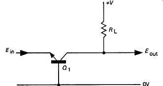
FIG1 Simple grounded base transistor amplifier circuit
FIG2 Typical grounded base RF amplifier
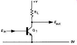
FIG3 Typical grounded emitter amplifier layout
The most common way of using a junction transistor as an amplifier is in the circuit layout shown in FIG3, where the emitter is returned to a low impedance point, and current is injected into the base. In this method of use, a much increased current will then flow in the collector circuit, so that f_c will typically be 50-500 times greater than f_b. This current increase, from base to collector, is called the 'current gain' of the transistor, and is known by the Greek symbol 'ß' (beta). [Please note that this is an entirely separate and distinct use of this symbol from that in feedback systems, described in Section 7.] To avoid this confusion, the 'common emitter current gain' of a transistor is more properly described as the hfe, where the quality described is the low frequency, or DC, value of this term, or h{Q -- using lower case letters -- where the current gain is measured at some (specified) higher frequency. The 'e' in this subscript refers to the fact that it’s the 'common emitter' characteristic which is measured. For example, hfe would be the term used to describe the 'common-base' figure, a (alpha).
The current gain of a transistor will decrease with increasing operating frequency, as shown in FIG4, and the frequency at which it decreases to unity is known as the 'transition frequency', or/T, sometimes also described as the 'gain-bandwidth product'. This tends to give a somewhat over-optimistic impression of the HF performance of a transistor, in that a device with a current gain of 200, and a 'transition frequency' of 300MHz, would, in reality, have a current gain value which would decrease, at a slope of 6dB/octave, beyond 1.5MHz.
The low frequency current gain also depends some what on collector current, in the manner shown in FIG5, but used as a current amplifier the transistor is a relatively linear device, and one of the ways by which the transistor's performance, as a voltage amplifier, can be made more linear is by inserting a large value of resistor between the signal source and the base of the device, as shown in FIG6. The problem with this method of use is, of course, that the gain of the stage is reduced, and its input noise figure worsened, by the presence of this added resistor. How ever, it does mean that a transistor voltage amplifying stage will be more linear in its operation -- other things being equal -- if its base is driven from a high impedance source, such as the collector circuit of a preceding transistor amplifying stage.
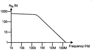
FIG4 Variation of hfe with frequency
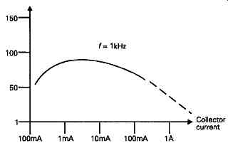
FIG5 Variation of hfe with collector current
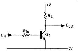
FIG6 Use of input swamp resistor to linearize current gain
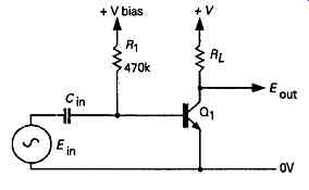
FIG7a Simple and unsatisfactory input biasing arrangement
Junction transistor voltage amplifiers
The simple circuit layout shown in FIG7a will act as a voltage amplifier, provided that the transistor is forward biased -- by a suitable current injected into its base, perhaps by the simple expedient of connecting a resistor, Rl9 between the base junction and some suit able voltage source -- into a condition where the collector DC voltage is somewhere between that of the collector DC supply rail and the collector saturation voltage of the transistor, which will probably be of the order of 0.2-0.5 V. Because the actual current gain of a transistor used in any given circuit design cannot be predicted in advance, and it’s poor design practice to offer a circuit for which the semiconductors must be pre-selected, the injection of some fixed value of base bias current won’t be a satisfactory answer to this requirement.
The repositioning of Rx between the collector and base junctions, as shown in FIG7b, will provide a simple, though crude, means of controlling the base bias current within fairly broad limits, since if the current gain of the device turns out to be high, and this leads to a high collector current- so that the collector potential falls towards 0.5 volts -- the bias current through R{ will similarly fall, while if the current gain is low, and the collector potential rises toward the supply rail voltage, because of inadequate collector current, the base bias current through Rx will also rise.
This is, however, a clumsy method of controlling the working conditions of the transistor, and suffers from the problem that, because of the effect of the internal negative feedback through R1 (see Section 7), the gain of such a stage can never exceed R1/Zm. In the circuit shown in FIG7b, this gain limit will be 47.
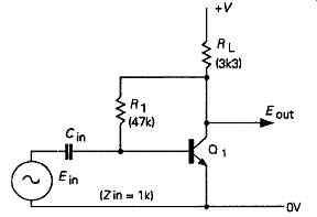
FIG7b Improved input biasing arrangement
A much more elegant method of biasing such a transistor amplifying stage is that shown in FIG8a, where the base is fed from a relatively low impedance potential divider, and the current through the transistor is controlled by the value chosen for the emitter resistor, R4.
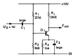
FIG8a More satisfactory method of biasing amplifier transistor.
For the circuit shown, ignoring the relatively small base bias current, the values shown in the drawing will set the collector current fairly precisely to 2mA, and the collector potential to a voltage about half way between the potential of the supply rail and the emitter voltage. Moreover, this set of DC conditions will be largely unaffected by the actual current gain of the transistor, over quite a wide range of likely values.
This arrangement has the drawback that there can be unwanted signal breakthrough into the input from the supply line. This problem can be avoided by the layout shown in FIG8b, where C2 is used to decouple the input bias circuit, at the cost of a somewhat greater component count. This input bias system can also be used with other circuits where an input bias voltage must be derived from the DC supply rail.
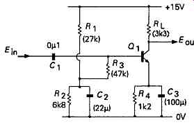
FIG8b Means of improving circuit loading and supply line ripple rejection
If a two stage amplifier circuit can be used, for example, as shown in FIG9, the use of DC negative feedback, through R4, can be used to stabilize the working conditions quite precisely, and it will again be almost independent of the actual current gains of the transistors used. For example, for the resistor values quoted, the base potential of Q1 will be 8.25V, its collector current will be 0.18mA, the collector current of Q2 will be 6.5 m A, and its collector potential will be 6.5 V DC, allowing an output voltage swing of some 14V peak to peak. If the current gains of the transistors are low, the output DC potential will fall, though only by 0.1-0.2V, and this will increase the current through 7?4, and cause the collector currents of both Q1 and Q2 to increase, and conversely.
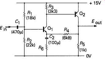
FIG9 THY; stage amplifier with NFB used to stabilize both gain and working
point
An amplifier stage of this type will probably have a voltage gain of some 2000, provided that C2 has a large enough value. A more precise control of stage gain can be obtained by inserting a resistor, Re, in series with C2. The gain, for reasons explained in the next section, will then approximate to (R6 + R4)/R6, for gain values which are small relative to 2000. This particular circuit layout makes a very useful and versatile gain block, and shows the convenience of being able to use a PNP transistor in combination with an NPN type, to be able to avoid the need for DC blocking inter-stage coupling capacitors.
A comparable circuit layout, using only NPN transistors, is shown in FIG10. This has a somewhat higher intrinsic gain, though with a rather less good stability of DC operating conditions. If C2 is removed, the stage gain is then controlled by the values of R4 and R5, and is, approximately, (R4 + R5)/R5, over a wide frequency range. Both of the circuit layouts of FIGs 9 and 6.10, give very much lower levels of harmonic distortion than either of the earlier single transistor circuit layouts.
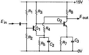
FIG10 Two stage feedback amplifier using only NPN transistors
The circuit layout of FIG10 can be elaborated to make a three-transistor layout of the kind shown in FIG11, in which the two transistor amplifier stages, Q1 and Q2, are followed by an impedance converting, 'emitter follower' stage, ß3, which makes the gain of Q2 independent of the load impedance applied to the output of the circuit. Both DC and AC negative feedback are applied through R6 and R4, to stabilize the (AC) working gain of the circuit, as well as its DC operating conditions. If R4 is partially, or wholly bypassed by a capacitor (C2), the gain can be adjusted, up to a possible figure of 10,000, with high gain transistors.
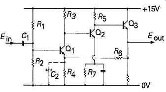
FIG11 Three stage feedback amplifier with emitter-follower output
Transistor stage gain and distortion:
One of the minor inconveniences of the junction transistor, as a voltage amplifier, is that its base voltage/collector current relationship is very non-linear, as shown in FIG12a, by comparison, for example, with a typical grid voltage/anode current characteristics of a thermionic valve, shown, for comparison, in FIG12b.
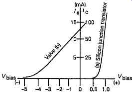
FIG12 Relative input transfer characteristics of junction transistor versus
valve.
Several aspects of transistor behavior can be seen from FIG12a, of which the first is that the rate of change of collector current, for an increment in base voltage -- known as the slope or mutual conductance, and denoted by the symbol gnv measured in amperes (or milliamperes)/volt, now known as 'Siemens' (or mS) -- increases rapidly with increasing collector cur rent. The theoretical formula, from which the mutual conductance of a junction transistor can be derived, is:
gm=Ic(q/kT) (1)
…where Jc is the collector current, q is the electronic charge in coulombs, (1.6 x 10^19), k is Boltzmann's constant, (1.38 x10^ 23), and T is the absolute temperature of the junction, in °Kelvin. For most modern silicon planar small signal transistors, this gives values of gnv in the range 25-40mA/V, per milliampere of collector current.
A simple approximation to the low frequency volt age gain of a transistor amplifier stage, of the type shown in FIG8, is given by the relationship:
Stage gain = gmR1 (2)
Where R1 is the effective load impedance of the circuit, which would be nearly 3k3 in the case of FIG8a.
So, for a collector current of 2mA, this circuit should give a voltage gain of about 150-250, if it’s driven from a low enough source impedance and if both C1 and C2 are adequately low in impedance at the chosen operating frequency.
The second characteristic which can be deduced from FIG12a is that there will be a substantial amount of distortion in the amplified output signal, because of the curvature of the Vy/C relationship.
However, any curve will approximate to a straight line if a small enough segment of it’s taken. This means that if the input signal is small enough, the distortion given by the stage will also be small. This is more or less independent of the actual gain, and the consequent output voltage, given by the stage, since the relation ship between collector voltage and collector current, for any given base voltage setting, as shown in FIG13, is, in fact, quite flat. However, the simple expedient of increasing the collector load resistor, to increase the stage gain, suffers from the drawback that the collector current would also have to be reduced -- unless the supply rail voltage can be proportionally increased-- to maintain the chosen DC collector potential, and this would reduce the effective 'slope' of the transistor, which would lessen the expected increase in stage gain. If, however, some arrangement can be found which would provide a high collector load impedance, while still allowing a moderately high working collector current, without the need for impracticably high supply rail voltages, a very much higher stage gain could be obtained from a single transistor amplifier stage. Moreover, because this would require only a very small input signal voltage, it would also give a very low level of signal distortion.
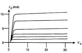
FIG13 Collector current/voltage relationship Circuits of this type have
been designed, (JLH, Wireless World, Sept. 1971) and are offered commercially,
in IC versions, such as the LM359. The operation of these circuits will be
examined later in this section.
DC amplifier layouts:
All of the circuit layouts so far described have been aimed specifically at the amplification of alternating signal voltages, in which any direct voltage component has been blocked of f by the inclusion of a DC blocking capacitor in the signal line. If, however, a+/ pair of supply voltage rails is available, so that the emitter of the transistor can be made about 0.6 V negative, in the case of an NPN device, the transistor can also be made to act as a DC amplifying stage, as shown in FIG14a. This would give a DC output voltage which would not normally sit at 0V, DC, for a 0V DC input potential.
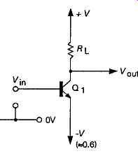
FIG14a Very simple DC amplifying stage
A simple elaboration of this circuit, shown in FIG14b, to include a zener diode (ZD1), in the output circuit could offset the normal +ve quiescent collector voltage of Q1? and allow an output voltage which was at 0 V DC, but the circuit would be highly susceptible to output voltage drift as the static base-emitter potential, and the collector current, varied with temperature.
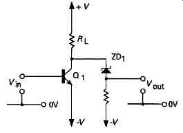
FIG14b Simple amplifying stage with DC offset minimized by zener diode
A useful circuit layout which allows automatic compensation for the temperature dependence of the base emitter potential of Q1 is that known as the long-tailed pair, shown in FIG15a, where if a matched pair of transistors is used, the current through Q2 will be the same as that through Q1, and any changes in base-emitter voltage will apply equally to both transistors, and will merely result in a change in emitter voltage to sustain the existing collector currents through Q1 and Q2.
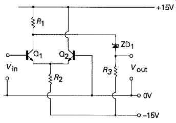
FIG15a Input long-tailed pair arrangement
Once again, a zener diode could be used to offset the static DC potential on Q1 collector, to give the required zero output level for zero DC input potential. How ever, a much neater arrangement is that shown in FIG15b, where a PNP transistor is used to give additional amplification, and invert the output current flow, so that the potential drop across R5 can give a true OV DC output. The AC and DC gain is then set by the choice of the feedback resistors R3 and R4, to give a figure which will be very close to (R3+R4)/R3 in value. For high values of R{> so long as the current gain of Q3 remains constant, the actual base-emitter potential of Q3 is relatively unimportant since Q3 is current rather than voltage driven.
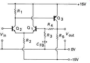
FIG15b Improved DC amplifier circuit based on an input long-tailed pair.
Although this circuit is capable of use as a DC amplifying stage, and, indeed, forms the basic type of input circuit used in almost all the opamp integrated circuits, some of which are specified especially for DC amplification, its other qualities, such as low distortion arid stable performance characteristics, commend it for use as an AC amplifier, in which use, a capacitor, Ca, , will be inserted in series with R3. This has the effect of making the circuit have a unity gain, at DC, so that the quiescent output voltage will be accurately equal to the quiescent input voltage, while giving a stage gain of (R3+R4)/R3 at all frequencies where the circuit 'open-loop* gain is high enough, and the impedance of Ca , is small enough to be ignored.
Constant current sources and current mirrors:
As mentioned earlier, it’s very useful to be able to operate a transistor with a high load impedance with-out also needing to limit the actual value of collector current employed, since reducing the collector current would reduce the operating 'slope' of the transistor, and thereby lose some of the extra stage gain which the use of a higher load impedance was intended to provide. The simplest answer to this need is to use a circuit arrangement known as a 'constant current source'. As its name implies, such a circuit would provide a constant output current over a wide range of applied voltages, and, in its simplest form would just be the collector circuit of a transistor operated at a fixed forward bias.
A practical version of this is as shown in FIG16, where, for the reason shown in FIG13, the collector current is largely unaffected by collector voltage, so that the circuit behaves as if it were a very high resistance connected to a sufficiently large negative potential to cause the measured current flow, but with, in reality, only a modest supply voltage requirement.
The circuit of FIG16 works best with a fairly large value of both VK{ and R2, but this limits the minimum voltage drop at which the circuit can be used.
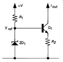
FIG16
Because of the usefulness of such constant current sources, a wide range of circuits has been evolved for this purpose, of which one of the most effective is the layout shown in FIG17. In this, if the voltage drop across R2 exceeds the voltage required to force QY into conduction, the collector current of Q{ will 'steal' the current which would otherwise flow through Rx into Q2 base -- which will, in turn, reduce the current flow through Q2 and R2. This circuit has a high dynamic impedance, and will also operate at a relatively low voltage drop across Q2/^2 ~ ~ down to a little above 1.2V.
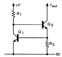
FIG17
A very common, contemporary form of constant current source is the two-terminal version based on a field effect transistor, and shown in FIG18. The method of operation of this type of device is explained later in this section, under the heading 'Junction FETs'. This type of device offers a very high dynamic impedance, at a range of specified operating currents, but has, usually, a more restricted maximum working voltage than a layout of the types shown in FIGs 16 and 6.17, based on small signal bipolar transistors.
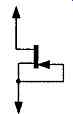
FIG18 FET constant current source
(Note. It’s customary for all of these circuits to be called constant current 'sources', though this would only be true where they were operated from a more negative supply rail than their load-- where one defines 'current' as the flow of electrons, as I have done throughout this guide. For accuracy in terminology, therefore, where such circuits are connected between the operating system and the positive supply rail, they should be referred to as constant current 'drains'. Luckily, the term 'constant current source' is accept able in both -ve and +ve supply rail applications.)
'Current mirrors' are a special class of high dynamic impedance constant current sources, in that their out put current is dependent upon some arbitrarily chosen input current, and in which the output current usually is chosen to 'mirror' the input one.
The simplest circuit arrangement of this type is that shown in FIG19, in which Q1 and Q2 are closely matched transistors, so that the current drawn from Q1 establishes a forward base bias for both Q1 and Q2 which will be, ignoring the small base currents drawn from both Q1 and Q2, of the correct value for the two collector currents to be identical. This circuit configuration is also available as a 'three terminal' IC pack age, for which types are available in which /out = Im, or = 2/ül , or = 0.5/hl, and so on, depending on user requirements.
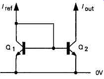
FIG19 Current mirror
A more sophisticated discrete component current mirror circuit is shown in FIG20, in which Q3 is added as a buffer to remove the base currents of Q1 and Q2 from the current drawn from the input. Where matched transistors are not available, the degree of current matching can be improved by inserting small value resistors between the emitters of Q1 and Q2 and the supply rail. As with 'constant current sources', these circuits are employed with both -ve and +ve supply rails.
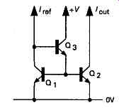
FIG20 improved current mirror
A typical application of a current mirror is as a high impedance load for a long-tailed pair input stage, such as that shown in FIG15b, redrawn, in FIG21, to include, in addition, a pair of constant current sources, of the type shown in FIG16, in place of the load resistors R2 and R5. The different currents required by the input and output transistors are arranged by the choice of different values for R1 and R5.
The higher dynamic impedance of Q3 than Q2, in FIG15b, gives very much better rejection of any unwanted supply line ripple on the -ve DC rail, and the higher impedance of Q7 than R5, in FIG15b, greatly increases the gain, and linearity of the output transistor (Q6).
Optional connections
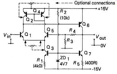
FIG21 Circuit arrangement using constant current source to supply a long-tailed
pair and a current mirror as its collector load The use of the current mirror
Q2/Q4 in place of the simple load resistor (R{ in FIG15b) has a number of
beneficial effects. Firstly, it allows the collector current of Q1 to be
chosen at a high enough value to obtain a good stage gain from Q1. Secondly,
it improves the linearity of Q1 as an amplifier stage.
Thirdly, it combines the output currents of both Q1 and Q5, and thereby improves the symmetry of the input stage -- as well as effectively doubling its gain -- and finally, it also improves the rejection of unwanted supply line ripple.
An additional feature of this type of circuitry is that it greatly minimizes the usage of resistors in the de sign, and this is of great value to the manufacturers of ICs, in which transistors and diodes are easy to fabricate, and not very demanding of 'chip' area, whereas resistors are more difficult to make with any degree of precision, and are relatively extravagant in their use of chip space.
Circuitry of the kind shown in FIG21 is representative of much contemporary low-frequency amplifier design, though, in order to increase the avail-able output voltage swing from Q6, it’s more usual for the constant current source, Q7/R5, to be replaced by a circuit of the kind shown in FIG17.
Where the circuit layout shown in FIG21 is to be used for DC amplification, as could be the case with IC opamps, provision is usually made for some form of output DC 'offset' zero adjustment, either by an external potentiometer connected between the collectors of Q2 and Q4, or, less commonly, by an offset adjustment potentiometer in the emitter circuit of Qt and Q5, as shown in dotted lines in the diagram.
It will be appreciated that the whole circuit layout shown in FIG21 can be inverted, by the use of PNP transistors in place of NPN types, and vice versa, and by altering the polarities of the supply rails. This could have certain advantages in practice, in that Q6 might, more advantageously, be an NPN device, in that these devices are better suited as higher power output transistors.
Similarly, the use of PNP transistors for the input long-tailed pair (Qj/C^), would give a somewhat lower input noise level, because the N type base region of a PNP transistor suffers less from recombination noise, and its 'base spreading resistance' will usually be lower, with lower associated thermal noise.
Since current mirrors and constant current sources are so common a feature of circuit design, the symbols of FIGs 22a, and 6.22b are widely used as a draughtsman's 'shorthand' for the circuit layouts of FIGs 16-6.18, and of FIGs 19 and 6.20 respectively. Using this notation, a very high gain single transistor stage can be formed from the simple combi nation shown in FIG23, of an amplifying transistor and a high impedance constant current load. This circuit arrangement would, however, suffer from two major practical drawbacks -- it would only give the expected high gain figure if any output load, ZL, had an impedance which was very large in relation to both the dynamic impedance of the constant current source and the output impedance of the amplifying device, and if the operating frequency was so low that the shunt impedances of any stray capacitance, both from the collector of Q{ to ground, and, more importantly, to Q{ base, could be neglected. In practice this would impose severe constraints on the performance of such a circuit.

FIG22 a. Constant current source; b. Current mirror
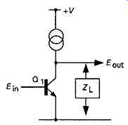
FIG23 Very high gain stage using constant current load for a transistor
amplifier
Impedance conversion stages:
The simplest form of impedance conversion stage is the emitter follower, shown in FIG24. The method of operation of this circuit is that, on switch on, an increasing current will flow through Rx until a potential is reached at which the base-emitter potential is just sufficient to sustain that value of emitter current. If the base voltage is increased, this equilibrium state will be disturbed, and the emitter current and emitter potential will also increase to restore the equilibrium. Similarly, if the base voltage is caused to fall, the emitter voltage will also fall, and this change in output voltage will occur, in either direction, as rapidly as the internal carrier creation or recombination processes within the transistor, or the external circuit capacitances, will allow.
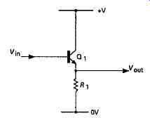
FIG24 Simple emitter follower
From a DC point of view, in the case of the NPN transistor shown, the output voltage will be the input potential less the forward base bias potential required to make the transistor conduct- typically 0.55 -- 0.6V, depending on emitter current. Similarly, for a PNP transistor, the emitter voltage will be more positive than that present on the base.
From the AC, or 'dynamic' point of view, for small signals, the input impedance of such a circuit will be high ...
[Zfa = Ä1(Afe+l)]
...and the output impedance will be low ...
The performance of such a circuit can be improved still further by the use of the circuit elaborations shown in FIGs 25a and 6.25b, known respectively as a 'Darlington pair' and a 'compound emitter follower', both of which arrangements can, of course, be used in their 'complementary' -- PNP vs. NPN -- forms. In both of these cases, the effective current gain, for the purposes of equations (3) and (4) approaches the product of the current gains of the two transistors. The circuit layout of FIG25b is superior from the standpoint of DC operation because it has only one base-emitter junction potential between the input and the output lines, and so suffers from only half the potential DC thermal drift.
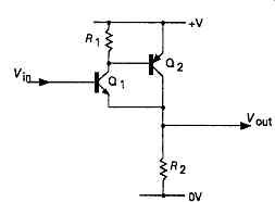
FIG25b Compound emitter follower
In both of the arrangements shown, there is a degree of asymmetry, in that the ability of the circuit to source current (through R2), is usually very much less than its ability to sink it (through Q1 and Q2). This asymmetry in single-ended emitter followers is particularly apparent where such an emitter follower stage is required to drive a capacitative load, where, if there is a rapid change in input voltage, the output waveform could show very different 'rise' and 'fall' times, as shown in FIG26, for the case of a square-wave input wave form.
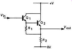
FIG25a Darlington pair emitter follower
FIG26 Effect of asymmetry of circuits FIG25 when used to drive a capacitive
load
For audio amplifiers, where it’s normally required to provide a symmetrical output impedance conversion stage between the voltage amplification circuitry and the low impedance loudspeaker load, a balanced pair of emitter followers will normally be used, such as that shown schematically in FIG27, and this will also avoid the problem of output waveform asymmetry.
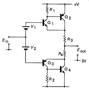
FIG27 Typical symmetrical emitter follower
Some external bias source, such as the notional pair of batteries, V{ and V2, will be required to cause the transistors to pass an adequate quiescent current to avoid conspicuous 'crossover' phenomena at the point where one pair of transistors ceases to conduct, and the other pair takes over. Combining such an impedance converter stage with the voltage amplifier shown in circuit used in output stage of audio amplifier Figure 23 will greatly improve its performance in respect of the stray capacitances, and the shunting effect of the load impedance itself, but will still leave the problems, in respect of HF gain, associated with the 'Miller effect' of the collector-base internal capacitance of Q1# This arises because any change in collector (or base) potential will require the collector base capacitance to charge or discharge through either the base or the collector circuit. Moreover, the higher the stage gain, M, the greater the effect will be. So, if a capacitance, C_fb, exists between collector and base of the input device, the stage gain will cause the input capacitance, C_in to look like:
…and symmetry would argue that the capacitance, seen at the collector, when the base was returned to a low impedance source, would appear to be the same.
A further, incidental, advantage of the long tailed pair circuit shown in FIG15a, if the output signal is taken from the collector circuit of Q2, as shown in FIG28, is that the dynamic input capacitance of Q1 is not increased by the Miller effect, and this allows this circuit to be used for HF amplifier stages.
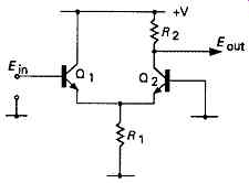
FIG28 Use of long-tailed pair input circuit to avoid loss of HF gain due
to Miller effect ?

FIG29 Cascode amplifier connection.
Cascode connection:
The problem of the unwanted effects of collector-base out capacitance is most satisfactorily remedied by connecting a pair of transistors in cascade, referred to, in electronic engineers jargon, as a 'cascode' connection.
Taking the simple circuit of FIG29, the input impedance offered by the emitter of Q2 is so low that its potential will vary by very little over quite a significant change in emitter-collector current. The input capacitance seen at the input of Q1 will therefore just be the sum of the static base-emitter and base collector capacitances, not modified by the voltage gain of Q1, because, effectively, this is nearly zero. In the case of Q2, if the base j unction is returned to a point offering a low impedance to AC, it will act as an electrostatic screen between its collector and emitter, and the only reactance seen at Q2 collector will be that of its normal internal collector-base capacitance. So, if the circuit of FIG23 is rearranged to use an input cascode stage, combined with an output emitter follower, as shown in FIG30, a very high stage gain can be obtained, up to perhaps 20,000 at 1kHz, coupled with an extremely low level of harmonic distortion -- even in the absence of external distortion reducing 'negative feedback' loops -- due to the fact that exceedingly small base-emitter voltage excursions are required to provide the desired output voltage swing, and over such very small excursions the base voltage/current characteristics of the junction transistor are quite linear.
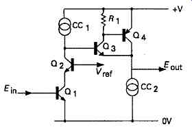
FIG30 Very high gain, low distortion amplifier circuit
One of the easiest ways of achieving this requirement is to use a single high-gain transistor with identical resistive loads in its emitter and collector circuits, as shown in FIG33a. The pair of 'anti-phase' output voltages generated by this circuit will then be virtually identical, since the collector current will only differ from the emitter current by the loss of the base current, which could well be less than one two hundredth of the whole.