AMAZON multi-meters discounts AMAZON oscilloscope discounts
Junction transistor manufacturing techniques
Having established in the early 1950s that it was possible to make 'solid state' semiconductor devices which would perform many of the same circuit functions as the existing thermionic tubes or 'valves', but with many advantages in size and power consumption, progress since that time has largely been in the development of constructional techniques giving lower manufacturing costs, improved performance, and greater reproducibility and reliability.
Early junction transistors endeavored to simulate, though with rather more fully controlled manufacturing processes, the basic structure of the early point-contact devices, but with the points brought towards each other on the opposite sides of a semiconductor slice, as shown in FIG. 1a, into cavities which had been etched to cause a local reduction in the effective thickness of the slice.
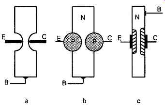
FIG. 1 Early PNP junction transistor
Since the positional stability of point contacts is not very good under conditions of mechanical vibration, a manufacturing processes manufacturing improvement was made by replacing these by infilling the cavities with a material (indium in the case of a germanium transistor) which would produce, by local surface diffusion, a pair of P regions on either side of the N type base, as shown in FIG. 1b.
There are obvious difficulties in controlling the depth of an etched cavity so that the residual base thickness -- which will determine both the current gain and the HF performance of the device -- is precisely constant from one device to another during a production run. A further improvement was therefore evolved, in which the required P type impurities were simply deposited on opposed areas of a thin flat slice, which was then heated to cause these dopants to diffuse inwards to the required extent, as shown in FIG. 1c.
The problems with this approach were that the silicon slice needed to be very thin to start with, which meant that it would also be fragile, and that if the device ran hot in use, the P type junction regions would continue to diffuse towards each other, causing the current gain of the device to increase, and its break down voltage to reduce, until the two regions eventually met in the middle, and the device became defunct.
The other shortcoming of all these approaches was that such devices were made on a 'one off' basis, whereas what was needed was a technique which allowed a large number of devices to be made, simultaneously, on the same semiconductor crystal slice.
This was accomplished by the introduction, in 1960, of the 'planar' manufacturing technique, by the Fair child Instrument Corporation, in the USA. In this process, by the use of photo-lithography, selected areas of the slice were exposed through apertures in a protective mask, and dopants were allowed to diffuse inwards, to produce, for example, on an N type silicon wafer, a series of flat bottomed P doped base * wells', into which a further series of N+ type dopants could be diffused to produce the emitter regions, as shown in FIG. 2. The silicon wafer can then be sliced into individual transistor segments, known as 'dies', by a diamond cutting wheel.
This masking and diffusion process could be carried out to produce, side-by-side, as many transistors as the size of the slice or the skill of mask production would allow, and this greatly reduced the cost of the individual devices.
The planar system is particularly suited to use with silicon, since it can easily be oxidized to silica, which is an excellent insulator, and is also an effective resistor to limit the areas affected by the added vapor phase dopants. The planar process allows the production of both PNP and NPN devices, of which the current gains and breakdown voltages are readily controllable.

FIG. 2 The planar manufacturing process for multiple transistors on a single
slice of silicon.
An improvement on this process, introduced in 1962, was the so-called 'epitaxial' system, in which the silicon wafer, after grinding and polishing, is ex posed to an atmosphere of hydrogen and silicon tetrachloride, at a temperature of some 1200° C, so that a thin monocrystalline layer of silicon, containing appropriate traces of dopant impurity, will be grown on the surface of , and with an identical crystal structure to, the single crystal silicon substrate. The masking process is then only required to define the regions through which the N+ impurities would be diffused into, say, a P type epitaxial layer on an N type substrate, to produce a series of NPN transistors.
It will be appreciated that the performance of a junction transistor is greatly affected by the characteristics of the base region. For this reason, the 'planar epitaxial' technique is now by far the most commonly used manufacturing process, because it avoids the need for the base region to contain both N and P type impurities, which arise in the planar process when, for example, a P type dopant is diffused into a region which already has an existing N type impurity.
In order to lower the conducting resistance of the relatively thick collector region, it’s customary to diffuse a more heavily doped layer into the reverse side of the slice, to produce a P+ region in a PNP device, and an N+ layer in an NPN one, as illustrated in FIG. 3.
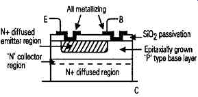
FIG. 3 Epitaxial planar transistor structure
The 'ohmic' connection to the collector will normally be made by soldering the individual dies onto metal 'header' tabs and connections to the emitter and base regions will be made by vacuum deposition of aluminum through apertures in the upper 'passivating' layer of silica, so that they make contact with the appropriate exposed semiconductor regions, as is also shown in FIG. 3.
The typical dimensions of the die used for a small signal transistor are 0.5mm square, ranging up to about 4mm square for a high power device. In order to conduct heat away from the junction regions, the slice thickness is kept as small as possible compatible with ease of handling and freedom from breakage. Values of 0.15 -- 0.5mm are typical.
Junction transistor characteristics
The major difference in use between a thermionic valve and a junction transistor is that the transistor is a current operated device, with a relatively low input (base-emitter) impedance, whereas the valve is a volt age operated component, with a very high input impedance. Moreover, while for quite a large part of its usable input voltage range, the valve has a quite linear relationship between input (Gi) voltage and anode current, this is not true for the junction transistor, which has very nonlinear input voltage vs. output current transfer characteristics. This arises partly because the relation ship between base-emitter voltage and base current is nonlinear, of the general form shown in FIG. 4, and partly because the common-emitter current gain (beta) is influenced by collector current, being lower at very small and large values of collector current than at some intermediate current levels, as shown in FIG. 5.
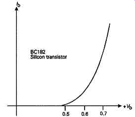
FIG. 4 Relationship between base current and base voltage injunction transistor.
Note: BC182 Silicon transistor
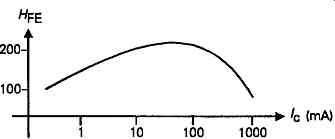
FIG. 5 Relationship between current-gain and collector current in silicon
junction transistor
For these reasons, the use of a transistor as a voltage amplifier, in the circuit shown in FIG. 6, would lead to substantial distortion in the output waveform.
Care must therefore be taken in the design of transistor voltage amplifiers to minimize the undesirable effects of the device characteristics. To some extent, the linearity of the relationship between current gain and collector current can be helped by care in the design of the internal structure of the device, and recent device types are better than earlier ones.
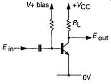
FIG. 6 Simple transistor voltage amplifier circuit.
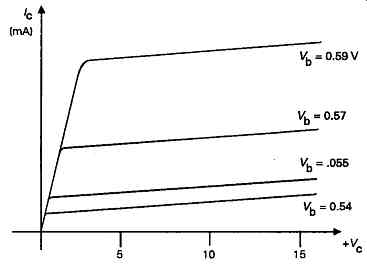
FIG. 7 Relationship between collector current and collector voltage for
small signal silicon transistor.
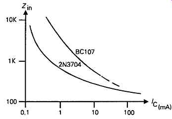
FIG. 8 Relationship between input impedance and collector current in silicon
junction transistors.
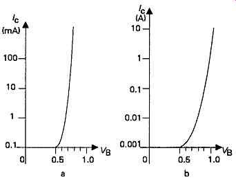 FIG. 9 Relationship between base voltage and collector current injunction
transistors.
The output impedance of the bipolar transistor is high, so that the relationship between collector current and collector voltage is typically as shown in FIG. 7, for a range of potentials applied to the base. This high output impedance characteristic is often of considerable benefit in bipolar transistor circuit design.
Under small-signal use, the input impedance of a junction transistor is dependent on the value of collector current, as shown in FIG. 8, as is also the 'noise figure* (the ratio, in dB, between the random noise introduced by the transistor, as an amplifier, and the thermal noise which would be expected from a perfect amplifier having the same input impedance), as discussed in greater detail in Section 16.
With thermionic valves, an important performance characteristic is the 'slope' of the input voltage vs. anode current curve. This is usually called the 'mutual conductance', gnv and expressed as mA/V, or, in con temporary terminology, milliSiemens (mS). Because of their very steep collector current turn-on characteristics, bipolar transistors have very high values of mutual conductance (/C/Vb), measured in Siemens (A/V), but this figure is not usually specified because it depends so strongly on collector current, (7C). This is shown for a small signal and a power transistor in the graphs of FIGs 9a and 9b. The theoretical relationship between mutual conductance and collector current is…where q is the charge on the electron, (1.60 x10^19), k is Boltzmann's constant, (1.38 x10^-23), and T is the absolute temperature. For a junction temperature of 25° C (298° K), this equation gives a calculated value of 38.9S/A. In practice, the actual value for gm in a transistor will be influenced by its construction. Typical values of 'mutual conductance' for silicon bipolar transistors, as a function of collector current, lie in the range 15-45 S/Ampere.
Because the junction transistor is a conductive element, in which the output and input circuits will interact with one another, the relatively simple methods for calculating circuit performance which were used with thermionic valves were not of use with transistors.
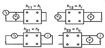
FIG. 10 Approach to derivation of h parameters.
A more fundamental approach was therefore adopted in which these devices were treated simply as four terminal 'black boxes', as shown in FIG. 10, in which the relationships between the input and out put circuits could be specified in terms of their mutual impedance (Z) or admittance (Y) parameters.
With growing familiarity in the use of these by circuit engineers it was found that some of these parameters were more useful than others, and so a combination of these, known as 'hybrid' or h parameters, has become almost universally adopted.
In these, h1 is the input impedance, and is defined as ...
hi is the forward current transfer ratio, and is defined as ...both of these measured with the output voltage held constant, ho is the output admittance, and is defined as ...
... and hT is the voltage feedback ratio, defined as ...
.... both of these as measured with the input circuit open circuit (o/c) to AC. The numerical value of these parameters will vary, depending on whether the transistor is connected in the 'common emitter' (emitter returned to a neutral no signal line), 'common collector', or 'common base' configurations, and the condition for which the parameter is defined will be denoted by the subscript. For example, if the 'forward current transfer ratio' -- commonly known as the 'current gain' -- were to be specified for a transistor connected, as it would normally be, in the common emitter mode, the symbol Af e would be employed.
Another convention is that an upper case (capital) subscript is used to denote the large signal, or DC value, of this characteristic. If the small signal value is intended, as, again, would normally be the case, the subscript to the h symbol is written in the lower case, so a numerical value quoted for Af e means the 'small signal current gain, for a transistor connected in the common emitter configuration'.
From the published values for these parameters, the circuit performance may be calculated. For example, the stage gain given by a junction transistor in the circuit of FIG. 11 can be derived from the equation:
... where Rs is the source resistance, R1 is the load, and r_i is the internal (base/emitter) impedance of the transistor.
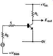
FIG. 11 Transistor stage gain model.
The last of the commonly published performance parameters relates to the high frequency performance of the device. Because of the finite time which it will take an electron or a hole to cross the base region of the transistor, and because of the effect of base-emitter and base-collector junction capacitance, in combination with the finite base input impedance of the device, the effective current gain will decrease with increasing frequency. This is specified as the 'transition frequency', or 'common emitter gain-bandwidth product', f_t, which simply means the frequency by which the small-signal current gain of a transistor amplifier stage, using a circuit layout in which its emitter is connected to an AC neutral line, will have decreased to unity.
This method of specification tends to give an over generous impression of the HF performance of the device, since a quoted value of ft = 300MHz, for a small signal transistor with an Af e of 300, will imply that the current gain of the transistor will have fallen to 150, at 2MHz, to 30 at 10MHz, and to 5 at 60MHz.
Thermal effects
The other characteristic of the bipolar junction device which must be considered is that the junction transistor is a temperature dependent device, in that both the forward base-emitter voltage and the collector emitter breakdown voltage decrease with temperature.
Not only does this determine the maximum working temperature which is permissible with the device, but it also controls the permitted thermal dissipation of the junction, for any given die size, and for any given thermal conductivity through the mounting substrate to free air, or to some external 'heat sink'. A specific problem which arises with all these devices is that the emitter current (and hence the collector current) for any input voltage, will depend on the temperature of the base/emitter junction. If this becomes hotter, more current will flow, and the device dissipation will increase, making the base/emitter junction still hotter.
This problem is particularly acute in power transistors with a large junction area, in that, if one small region of the base/emitter junction should become hotter than the rest, its forward voltage will decrease, in comparison with the remainder of the junction, and this will cause the total device current to be funneled through this small section of the device, heating this small local region still further.
To avoid the possibility of device failure due to this cause, manufacturers specify the limits of the 'safe operating area' (or SOA) for all power devices, in the form shown in FIG. 12. Meanwhile, care should be taken in all transistor circuit design to ensure that the dissipation of the devices stays within the specified limits. If long device life expectancies are required, the thermal safety margins should be generous.
Junction field effect transistors (FETs)
These devices utilize semiconductor junction technology to construct a type of transistor which has very similar characteristics to those of a thermionic valve, but without the need for a heated cathode or a relatively high supply line voltage.
The method of construction is shown in FIG. 13, and consists, in its essentials, of a thin slice of silicon into which a pair of gate regions, with a different type of doping to that of the substrate, have been diffused from opposite sides of the slice. If the slice is of N type silicon, and the diffused gate regions are of P type, as shown in FIG. 13a, the device is described as an N-channel FET. If the slice is P type, and the gate regions are N type, as shown in FIG. 13b, it will be called a P-channel FET. These two types of FET are substantially identical in characteristics, except that one operates from a +ve supply line, and requires a negative bias on its gate to cut of f the channel current, while the other operates from a -ve supply, and requires a +ve gate bias.
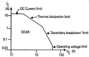
FIG. 12 Typical safe operating area curve for power transistor.
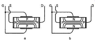
FIG. 13 Schematic construction of N- and P channel junction FET.
The method of operation of the FET is basically very simple. If the slice of semiconductor material has some suitable impurity content it will conduct electricity by electron or hole flow between ohmic contacts at either end of the slice. These contact regions are called the 'source' and the 'drain' respectively, and the conducting path between them is called the 'channel'. However, for reasons given in Section 4, when oppositely doped regions are formed on the slice, depletion zones will occur as a result of electron and hole diffusion, both within these regions, and within the slice, and in these regions, which have been depleted of carriers, no current will flow. That part of the slice which can carry the current is therefore reduced in thickness and the resistance of the channel is in creased. If the reverse bias on the gate regions is increased, the channel will be further narrowed. On the other hand, if it’s biased in a forward direction, the depletion zones will decrease, up to the point at which forward conduction of the gate occurs, as a simple junction diode.
This leads to the type of relationship between gate voltage and drain current shown in FIG. 14 for a typical N-channel junction FET. The curve for a P channel FET would be similar, but with reversed polarities.
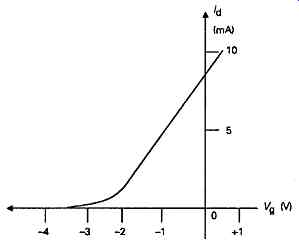
FIG. 14 Conduction characteristics of typical junction FET.
A further feature of the FET which must be noted is that, because there is a potential drop along the con ducting channel, from source to drain, the actual gate-channel potential will vary across its width, leading to an unsymmetrical depletion region, as shown in FIG. 15. As the drain-gate potential is increased, the depletion regions extend further towards each other until they meet, and 'pinch off' all current.
When this happens, the potential drop along the remainder of the channel, towards the source, disappears -- with a consequent widening of the conducting channel, apart from the narrow neck at the drain end, which becomes sufficiently short that electrons can still tunnel through it.
In this 'pinched-off' condition, the current through the FET is substantially constant, for any given gate source bias, over a wide range of source-drain potentials, as shown in FIG. 16. For a typical small-signal FET, pinch-off will occur at a relatively low drain-source potential (typically of the order of 2-3V), and because the FET has better performance characteristics when operated in this condition, especially because of its very high output impedance, FETs are usually employed at drain potentials which are greater than the pinch-off value.
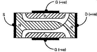
FIG. 15 Effect of pinch off in junction FET VH (V)
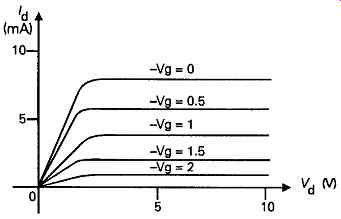
FIG. 16 Junction FET drain current characteristics at voltages above pinch
off.
The very flat /d/Vd characteristic of the junction FET, when used in this mode, is much more characteristic of a pentode valve than of a triode. Junction FETs do, however, have a fairly high gate-drain capacitance -- varying with gate-drain voltage, but in the range of several pF-- so they are not very useful, in the common source mode, as RF amplifiers, unless some form of 'neutralization' is employed.
Because of the much more linear character of the gate voltage/drain current curve, the distortion introduced by junction FET gain stages is much lower than for bipolar transistors. On the other hand, because the mutual conductance (gm) of the FET is very much lower -- values in the range 2 -- 10mS (mA/V) being typical -- the stage gain for the same value of load impedance will also be much lower. Also, because the FET has a very high input impedance, (up to a million megohms), in its normal reverse biased state, the thermal noise associated with this is higher than for a bipolar device. An exception to this is the case where the device is used in an application in which the source impedance is comparably high. In this case the noise figure of the FET will be better than that of a bipolar transistor in a similar application, as explained in Section 16.
Junction FETs are normally only found in small-signal forms, at drain-source voltage ratings below 40V, and with free air (maximum) dissipation figures of the order of 350mW. Although power FETs have been made, these have largely been superseded by MOSFET types, and are now seldom found.
Insulated gate field effect transistors These devices, most commonly known as 'MOSFETs' (metal oxide semiconductor field effect transistors) or sometimes as 'IGFETs' (insulated gate FETs), represent a relatively recent development of semiconductor technology, if only because the technical problems in their manufacture are severe, and satisfactory methods for overcoming these problems have taken time to evolve. Commercial devices of this type are almost exclusively fabricated from silicon, though a few VHF devices have been made using gallium arsenide.
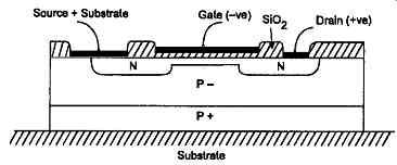
The basic idea behind the IGFET is a very simple one, and is illustrated in FIG. 17. It’s that if an electrostatic charge is brought into proximity to a body in which charge migration is possible, polarization will occur so that charges, of opposite sign to that inducing this polarization, will be drawn towards that face of the body which is closest to it, while charges of the same sign will be repelled away from it. This effect can be utilized in a practical device if the type of layout shown in FIG. 18a is adopted. In this a strip of P type material is formed on a P+ substrate, and a pair of N type zones are diffused into it at either end, to form source and drain connections. At the source contact, the metallization is extended to connect to the base/substrate as well, and a further metal contact, referred to as the gate, is deposited on a thin insulating layer formed between the source and drain regions.
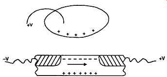
FIG. 17 Mechanism of electrostatic induction of mobile charges.
If a positive voltage is applied to the drain electrode, with respect to the source and substrate, no current will flow, because the substrate/drain P-N junction is a reverse biased diode, and there is no conducting path through the P- layer, between the source and drain, underneath the gate region, which forms, in effect, an NPN transistor with its base shorted to its emitter.
If, however, a positive charge is also applied to the gate metalizing, a layer of negative charges will be induced into the P- substrate, as shown in FIG. 18b, to form a link between the source and drain regions, and current will flow. Because this current flow is parallel to the surface of the silicon die, transistors of this type are called 'lateral' MOSFETs, to distinguish them from devices, such as bipolar transistors, where the current flow through the silicon die is 'vertical', that is to say, in a direction normal to the device surface.
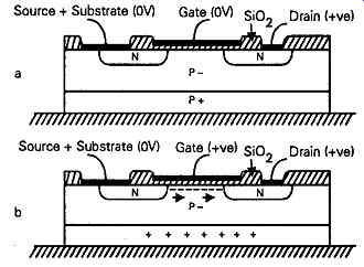
FIG. 18 Simple insulated gate FET. Source +, Substrate (0V) Gate (0V) $JQ
Drain (+ve).
This source/drain current will be directly proportional to the magnitude of the positive potential applied to the gate electrode, apart from minor effects due to the imperfect geometry of the system, and this leads to a very linear input voltage vs. output current transfer characteristic, as shown in FIG. 19.
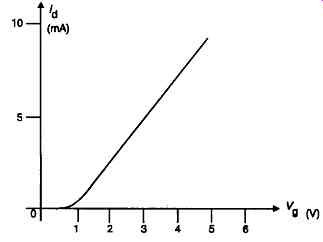
FIG. 19 Conduction characteristics of small signal MOSFET
Because the current flow is due to induced negative charges (electrons) and there is no current flow at zero gate voltage, such a device is known as an 'N-channel enhancement type MOSFET'.
If a thin layer of N type silicon is formed underneath the gate region during manufacture, as shown in FIG. 20, so that there is an already existing conductive path between the source and the drain, a negative charge applied to the gate will drive the N type carriers away, leading to an eventual cut-off of current al together when a sufficiently large negative gate potential is applied. This gives the type of transfer characteristic shown in FIG. 21, which is very similar in its form to that of a thermionic valve, and is probably even more linear in slope.
This kind of IGFET is called a 'lateral N-channel depletion MOSFET', and is typical of the small signal MOSFETs used particularly for HF amplification purposes.
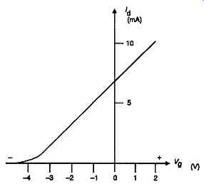
FIG. 21 Conduction characteristics of N channel depletion MOSFET
By using a complementary symmetry in the N and P type regions, P-channel MOSFETs can also be made, which have very similar electrical characteristics to the N-channel versions, and use the type of structure shown in FIG. 22. The circuit symbols used for these devices are shown in FIG. 23.
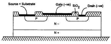
FIG. 22 Construction of lateral F-channel enhancement MOSFET
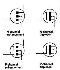
FIG. 23 MOSFET circuit symbols
The practical problems which delayed the realization of this type of transistor were mainly concerned with the production of a sufficiently thin and uniform layer of insulation between the gate electrode and the silicon die. The requirement being that a useful amount of current carrying charges could be induced into the channel at a sensibly low operating voltage, without this insulation being so fragile that inadvertently applied potentials would destroy it.
However, it was also necessary to maintain a very high degree of control over the chemical purity, and physical structure of the channel region, since any inadvertent contamination or crystal structure irregularity could lead to uncontrolled leakage currents.
Developments in manufacturing techniques, mainly evolved to allow the routine production of integrated circuits, have provided process systems which are well able to meet these needs so that reliable insulated gate FETs with repeatable device characteristics are now available at a modest cost.
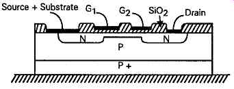
Dual-gate MOSFETs
As with triode valves, there is a significant inter-electrode capacitance between drain and gate, and this would cause instability, and possibly continuous oscillation, if such devices were used as simple RF amplifier stages. So, by analogy with the triode to tetrode elaboration, dual-gate MOSFETs are made, as shown in FIG. 24, with a second gate region between the signal gate (G1) and the drain. This effectively isolates G1 from the drain, and allows feedback capacitances as low as 0.02pF to be attained, so that such transistors can be used as stable high gain RF amplifiers. In straightforward RF amplifier use, such a transistor would normally be operated with a small negative potential (2-3V) applied to G1, since such dual-gate MOSFETs are usually depletion type devices, while G2 might be taken to a small positive potential, in the range 0-3V. However, the availability of this second control electrode allows the use of such a transistor in other circuit applications, such as mixers or frequency changers. Since dual-gate MOSFETs are principally used for HF/VHF applications, and the flow of electrons is very much more rapid than that of holes, these transistors are made exclusively as N-channel devices.
