AMAZON multi-meters discounts AMAZON oscilloscope discounts
MOSFET
Power MOSFETs Small signal transistors based on MOS technology give a very good HF response, since, in general, the rate of change of the conductivity of the channel is determined solely by how fast the input resistance and capacitance of the gate circuit will allow the gate potential to change.
Since this type of transistor ought, in principle, to work just as well in larger power versions, consider able technical effort has been directed, over the past decade, towards the production of power MOSFET devices which can be used as a replacement for the more sluggish bipolar power transistors.
The use of the 'lateral' MOSFET structure, shown in FIGs 18 and 20, is unsuitable for high current applications because the length and the shallowness of the current carrying channel leads to too large a path resistance. Early attempts to reduce the length of the channel, by restricting the width of the gate region, led to problems due to the limited precision of the photo lithographic processes by which the etching patterns are defined.
However, it was noted that in bipolar junction transistors the 'vertical' current flow path, from the emitter to the collector, is defined by the thickness of the diffused layers, as shown in FIG. 25a, and this thickness can be controlled with great accuracy.
So-called vertical MOSFET devices have therefore been produced, as shown in FIG. 25b, in which the source, channel and drain regions are formed as horizontal layers, as in a bipolar device, and a ' V shaped notch is then etched through these layers to allow an insulated gate electrode to be applied across the ex posed channel region. This gave rise to the description ' VMOS' for this type of device, though, because of the relatively high electrostatic stresses which arise at sharp points, the bottom of the notch is more usually flattened out, as shown in FIG. 25c. These devices are usually called 'U- MOSFETs', with reference to the 'notch' shape. Although this arrangement allows a much shorter effective channel length, the conducting resistance of the channel, even over this short vertical path, will still be relatively high, so, in order to achieve 'on' resistances equivalent to those of a bipolar power transistor, many such conducting channels need to be formed -- electrically in parallel -- on the same chip.
Various geometrical layouts have been adopted in order to provide a large number of parallel channel paths within a limited chip area, and one of the most elegant of these is that introduced by International Rectifier, Inc., in their 'Hexfet' range of power MOS FETs, although this is employed in a 'D-MOS' rather than a 'U-MOS' structure. In this design the masking, oxidation and etching pattern, used to define the dif fusion structure of the source and substrate regions, takes the form of a series of hexagonal pits, arranged in honeycomb fashion, as sketched in FIG. 26.
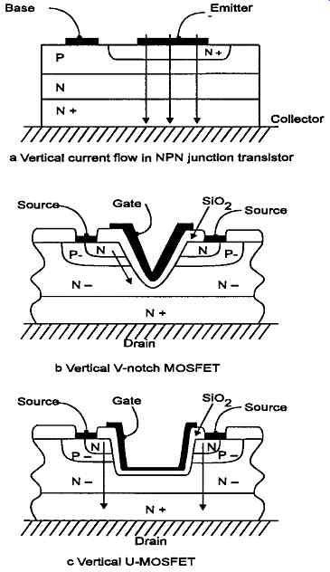
FIG. 25 Structures of various vertical MOSFET designs. A. Vertical current
flow in NPN junction transistor; a. Vertical current flow in NPN junction
transistor; c. Vertical U-MOSFET
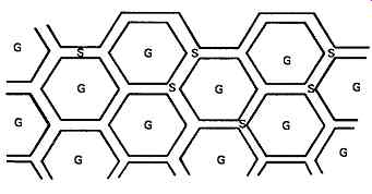
FIG. 26 Honeycomb structure used to provide multiple parallel gate channels
Channel resistances, specified as ' Rds (on)', as low as 0.02 ohms are now readily obtainable with power MOSFETs, as are operating voltages as high as 1200V, though at rather higher values of Rds (on). The 'U MOS' or 'V-MOS' type of construction lends itself more readily to N-channel MOSFETs, so the P-channel versions of these transistors are relatively more expensive, and offer a more limited range of working voltages and channel conductivities.
There are a number of practical difficulties in the use of these power MOSFET devices, of which the most immediately apparent is that the parallel connection of a number of gate regions leads to a high gate/source capacitance, and values for this in excess of InF are typical. This requires that the device must be driven from a low source impedance if good high frequency performance is required, in spite of the fact that the gate circuit is effectively an open circuit to DC. Another problem is that, because of the exceedingly fast internal electrical response of the transistor, high frequency parasitic oscillation can readily arise if the gate, source or drain connecting wires are long, or run parallel to one another. A *gate stopper' resistor, in the range 220-470 ohms, will usually serve to prevent this type of malfunction, which can often cause rapid destruction of the device.
Care must also be taken to ensure that the maximum gate/source voltage rating is not exceeded, since, if the gate insulating layer should break down, the device will be defunct. It’s common practice in small signal MOSFETs, such as the dual-gate types used for RF amplification, or in CMOS logic devices, for one or two Zener diodes to be diffused onto the MOSFET chip to act to limit excessive gate/source or gate/drain potentials. Unfortunately, this simple protective measure is inapplicable with power MOSFETs since it will cause the same layout of junction areas as is found in a thyristor, so that an applied gate voltage high enough to activate the protective diode could cause the whole device to trip into a short-circuit condition. Externally connected Zener diodes can usually be employed as protective components with out problems.
T-MOS devices
An alternative structure used for MOSFETs is that shown in FIG. 27, called T-MOS', from the conducting channel path shape, -- or also sometimes 'D-MOS' as a contraction of 'double-diffused, vertical current flow MOS'.
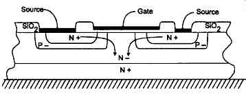
FIG. 27 Structures of T-MOS or D-MOS FET
These devices reflect the advances which have been made in manufacturing technology, in that they now use masking and etching processes to define very close tolerance channel lengths in a combination of lateral and vertical current flow, and offer the advantage that both N-channel and P-channel versions can be made, with less difficulty, although, even so, the N-channel versions are both more rugged and more suitable for high voltage use.
In principle, T-MOS devices are rather slower than the U-MOS versions, but the use of polycrystalline silicon gate electrodes, rather than deposited aluminum ones, has allowed the HF response to be improved to a value which is now not much lower than that of the V-MOS and U-MOS types.
With both U-MOS and T-MOS transistors there is a possibility of an excessive gate-drain voltage arising, at high drain potentials, since part of the gate insulation serves to separate the gate from the drain as well as from the channel. This danger is minimized, in the diffusion process, by arranging that that part of the drain region which is in proximity to the gate is of a very lightly doped (N- or P-) material. This is known as the 'drift' region, and, because of its relatively low conductivity, permits a relatively large voltage drop between the end of the channel and the highly doped (N+ or P+) substrate. The relative distribution of potential drops between the channel and this drift region is, however, influenced by drain current flow so that gate-drain breakdown can occur more easily at high device currents.
The drain current vs. drain voltage characteristics of MOSFET devices are similar to those of junction FETs, and are shown in the comparative graphs of FIGs 28 and 29.
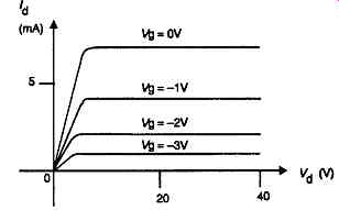
FIG. 28 Drain current characteristics of N-channel FET
With the major exception that some care must be exercised in circuit design and applications to ensure that the gate insulation layer breakdown voltage is not exceeded, MOSFETs offer a very valuable and versatile type of active component. In particular, the very good transfer, (Vin/Iout), and high frequency characteristics of these devices make them ideally suited for use in audio amplifier designs, and there are few such applications for which thermionic valves or bipolar transistors have been used, i n the past, which could not be performed better by one or other of the MOS type devices.
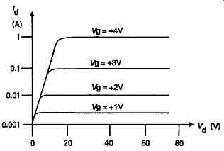
FIG. 29 Drain current characteristics of N'-channel D-MOSFET
Moreover, with the growing availability of P- channel devices, in addition to the well established N-channel versions, considerable scope exists for innovations in circuit design, using complementary polarities, which could never have been implemented with thermionic devices.
Also, whereas with both thermionic valves and junction FETs, in which both the grid and the gate electrodes will form a conductive path with the cathode or source, if it should become forward biased, the gate electrode of the MOSFET remains a high impedance point over its whole allowable voltage range. Again, the gate/source capacitance of the MOSFET is largely independent of the gate/source voltage.
A practical point which should be noted with all MOSFETs is that their method of manufacture, which employs a common connection to both an N and a P region at the source contact, as shown in FIGs 20, 22, 25 and 27, leads also to the formation of a parallel connected diode: a P-N diode in the case of an N-channel MOSFET, and an N-P diode in the case of an P-channel device. In normal use this diode is non-conducting.
Thyristors and triacs While power transistors exist which can handle large currents and voltages, in many cases all that is required is a semiconductor device which will operate as a low impedance switch. Indeed, a term which is sometimes used for one form of these components is 'silicon controlled switch'. In its simplest form, such a bistable semiconductor switch can be contrived by connecting a pair of PNP and NPN bipolar junction transistors, as shown in FIG. 30.
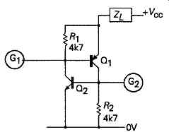
FIG. 30 Two transistor embodiment of thyristor
If Q1 is initially non-conducting, then no collector current due to Q1 will flow into Q2 base, so Q2 also will be non-conducting, and no collector current from Q2 will flow into Q1 base; a state of affairs which will continue as a conditionally stable state.
However, if a small current is injected into the bases of either Q1 or Q2, of such a polarity as to cause either of these to conduct momentarily, then both transistors will 'latch' into a stable conducting mode, with both devices being turned hard on. Some external current limiting components must exist, of course, to prevent the transistors from being damaged by this action.
So long as an adequate potential remains across such a regenerative pair of transistors, they will remain conducting, and can only be turned off again by either reducing the applied supply voltage to a level below that needed to cause conduction of the transistors, or by putting a short circuit across one or other of the base-emitter connections.
The use of a circuit of this type constructed from separate transistors is quite feasible, but since the current gains of both transistors will be much larger than is necessary to cause regenerative action, it’s prudent to connect a pair of resistors, as I have shown at R1 and R2, to prevent leakage currents from causing the circuit to trip inadvertently.
Such a PNP/NPN combination can be merged into a four-layer PNPN device, as shown in FIG. 31, in which the external connections are called the anode, cathode and gate terminals.
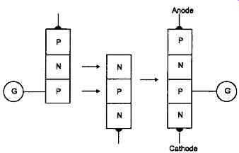
FIG. 31 Evolution of 4-layer SCR I thyristor from two transistors
With a practical four-layer switch, called a 'silicon controlled rectifier' (SCR), or 'reverse blocking triode thyristor', or simply a 'thyristor', the current gains of both of the incorporated transistors are chosen to be only slightly greater than unity, which helps both stability in use, and the ability of the device to operate at high applied voltages.
It’s an established convention that the gate connection will be that to the lower P type base region, (equivalent to Q2 base). Those SCRs with the gate connection made to the upper N type region (equivalent to Q1 base) are called 'complementary' SCRs.
The forward and reverse characteristics of the SCR are shown in FIG. 32, and a typical schematic cross-section, showing the disposition of the diffusion layers, is shown in FIG. 33. The circuit symbol used is that shown in FIG. 34.
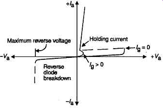
FIG. 32 Forward and reverse thyristor conduction characteristics
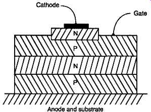
FIG. 33 Construction of practical reverse blocking thyristor.
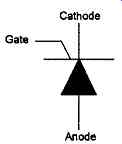
FIG. 34 Circuit symbol of thyristor.
Although many thyristor applications may be for relatively low power use, thyristors are intrinsically very robust devices. Depending on the die size, and the diffusion and heat-sinking arrangements, thyristors are available with peak current ratings of the order of thousands of amperes, and capable, if required, of holding of f potentials in excess of two thousand volts.
Since many of the uses of the SCR lie in the field of alternating current control, it would normally be used within a bridge rectifier layout, as shown in FIG. 35, in order to allow it always to switch in the correct polarity. However, a version of this device, known popularly as a 'triac' (triode AC switch), has been evolved to meet the specific need for an AC control component.
These devices can be visualized as a pair of PNPN and NPNP four-layer devices, joined in parallel, as shown in FIG. 36, with a gate electrode so arranged that it will be able to 'fire' either of these, as required.
This leads to the type of internal structure shown in FIG. 37 and the bi-directional turn-on characteristics shown in FIG. 38.
The circuit symbol for this AC switching device is shown in FIG. 39.
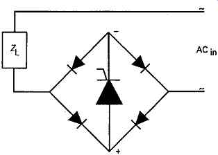
FIG. 35 Use of rectifier bridge to allow thyristor control of AC
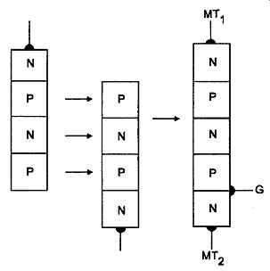
FIG. 36 Evolution of TRIAC from parallel connected thyristors
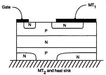
FIG. 37 Practical construction of triac
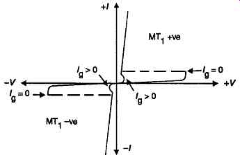
FIG. 38 Conduction characteristics of triac
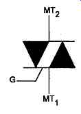
FIG. 39 Circuit symbol for triac
Silicon bilateral trigger diodes (diacs)
Proper operation of both SCRs and triacs is assisted if the turn-on voltage applied to the gate electrodes is in the form of a voltage pulse having a rapidly rising leading edge. This is most commonly achieved in practice by incorporating a small power switching element, which will suddenly break-over if its hold-off voltage is exceeded, in the input circuit to the gate electrode.
There are a number of devices which will serve this purpose, but the most common of these is the diac, which is basically an NPN junction transistor in which two identical N+ doped 'emitter type' junctions have been diffused on either side of the P type base layer.
When whichever of these junctions happens to be reverse biased is triggered into avalanche type break down, transistor action multiplies the resultant current flow, to give the type of conduction characteristics shown in FIG. 40.
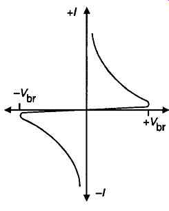
FIG. 40 Breakover characteristics of diac
Other trigger devices are also available, as are a wide range of variations of the basic thyristor/triac devices, to fit specific application needs. In general, all of these high power devices are relatively sluggish in operation, because of the time which is required for the current carriers to pass through the relatively thick N and P layers which are employed in their construction, and for the decay of the many minority carriers generated by the high conduction currents.
Because of the great utility of these switching de vices in power control applications, this has become an important branch of semiconductor technology, and there are many specialist manuals which give further information on this topic.
Linear integrated circuits If it can be said that, with the invention of the transistor, thermionic valves became obsolescent as amplifying devices, apart from certain specialized us ages, then it can be said, with equal truth, that the invention and successful development of the 'integrated circuit' has largely done the same for the discrete semiconductor. Indeed, it can be argued that it would usually be a wasteful exercise to employ many separate components and semiconductor de vices in order to achieve the same result that could be obtained, more cheaply, more predictably, more reliably, and in less space by a single IC block. It may often also be that the ready-made integrated circuit will offer a higher degree of optimization in design than the average engineer is likely to pursue for any one-off application.
This philosophy has encouraged the growth of 'application specific ICs' (ASICs), in which the design skills of the development laboratories of the semiconductor manufacturer are placed at the disposal of the engineer, even for applications in which the likely volume of sales is relatively small. However, the main forms of linear ICs remain the 'opamp.' gain blocks and voltage stabilizer circuits, discussed below.
Operational amplifiers (OPAMPs)
These are the universal low power gain stage units, commonly represented by the symbol shown in FIG. 41. These will typically require, for operation, a pair of positive and negative supply lines whose potentials will bracket the input signal voltage range. The recommended potential for these supply lines will normally be +/-15V, but the IC may operate, with some restrictions on possible output voltage swing and HF response, on supply line potentials as low as +/-3V.
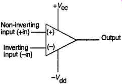
FIG. 41 Conventional circuit symbol for 'opamp.'
The output (peak-to-peak) voltage swing, obtain able without clipping, will usually be some 0.5V less than the supply line potentials, provided that the output frequency or current demand requirements are mod est. The circuit design is normally such that up to 100% negative feedback can be applied across the gain block without loop instability, usually manifest as HF oscillation, but this will depend on the specific IC type and the output load characteristics.
It’s taken for granted in modern opamp. ICs that internal protection circuitry will be incorporated which will prevent inadvertent damage through short circuits from the output connection to the 'OV line, or through excessive output current demands.
Developments in these devices are continually introduced, as a result of competition between manufacturers, so, provided that equipment is designed to accept ICs having conventional pin configurations, of the types shown in FIG. 42, equipment performance can often be upgraded simply by replacement of the existing ICs by those of more recent design.
Examples of the supply line requirements, and the performance specifications for two such units, representing 'second generation' and 'third generation' designs are shown in Tables 1 and 2.
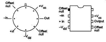
FIG. 42 Normal pin connections for single IC opamps -- shown from top of
package
===
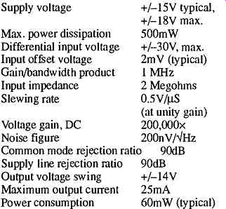
TBL. 1 Performance specification for '74G type IC amplifier unit
Supply voltage
Max. power dissipation Differential input voltage Input offset voltage Gain/bandwidth product Input impedance Slewing rate Voltage gain, DC Noise figure Common mode rejection ratio Supply line rejection ratio Output voltage swing Maximum output current Power consumption
+/-15V typical,
+/-18V max.
500mW
+/-30V, max.
2mV (typical)
1MHz 2 Megohms
0.5V/|LIS (at unity gain)
200,000x 200nV/VHz o 90dB
90dB
+/-14V
25mA
60mW (typical)
===
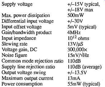
TBL. 2 Performance specification for 'LF351' type IC amplifier unit Supply
voltage Max. power dissipation Differential input voltage Input offset voltage
Gain/bandwidth product Input impedance Slewing rate Voltage gain, DC Noise
figure Common mode rejection ratio Supply line rejection ratio Output voltage
swing Maximum output current Power consumption
+/-15V typical,
+/-18V max 500mW
+/-30V 5mV (typical)
4MHz 1012
ohms 13V/|iS 300,000x 15nV/VHz 110dB (average)
+/-13.5V 13mA 55mW (typical)
===
Other operational amplifier designs have been evolved for specific end uses, such as the ??07' , which is intended particularly for low frequency instrumentation applications, in which the input DC offset voltage has been reduced to ??µF, and the input voltage drift with time is as low as 0.2µF/p?????. In the field of low-noise, low-distortion amplifiers, the ??27' offers a typical input noise figure of 3nV/VHz, coupled with an LF voltage gain figure of ?,???,???? , which allows harmonic distortion figures of the order of 0.002% at 1kHz, and 10V RMS output, at circuit gain values up to 100x.
For audio applications, the 'LM837' offers a slewing rate of 10?/µ5, a gain bandwidth product of 25MHz, and a power bandwidth of 200kHz, typical.
The input noise voltage of this device is 4.5nV/VHz, coupled with a THD figure, at up to 10kHz/6V RMS output of 0.0015%.
There are also ICs of this general type which are designed for use in high frequency applications, such as the '046165' family, which offer a gain bandwidth product of 725MHz, coupled with a slew rate of 300V/V S, although many of the very high speed devices are designed as unity gain buffer (impedance converter) stages or 'voltage followers'. Devices of this type, such as the 'LH0063\ offer a slew rate of 2400V^S, and a working bandwidth of DC-200MHz.
Voltage regulators
This is the other major field in which ICs have established a very wide presence in linear circuitry, because of the almost universal desirability of supply lines which are stable, and noise and ripple free, from which this circuitry can be operated.
These ICs are made in two main types, the so-called ' 3-terminal regulators' (available in both positive and negative supply line versions) which are designed to provide highly stable, overload proof, fixed output voltage sources, at a wide range of output voltage and current ratings, covering the range +/-5V to +/-24V, at current outputs of 100mA to 10A, and 'programmable voltage regulators'.
The programmable, or adjustable types are intended to confer the same performance benefits as the fixed voltage types, though with the added advantage of being able to vary the actual output voltage. If a small reduction in the performance of the voltage regulator is acceptable, it’s possible to achieve some adjustment of the output voltage by the simple expedient of inserting a variable resistor in the W return path of the IC. The normal ways of using these ICs are shown in FIG. 43. The circuitry employed for this type of application is discussed in greater detail in Section 15.
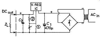
FIG. 43 1 normal method of use of voltage regulator IC, and 2 method of adjusting
output potential
Voltage reference devices
In addition to the voltage regulator ICs, there are also integrated circuit blocks which are intended to provide a high precision replacement for the zener or avalanche diodes. These will be used in similar circuitry to the normal 2-terminal regulator diode, but will offer a much higher degree of output voltage precision, and with much lower noise and output voltage drift as a function of time or ambient temperature.
Transistor and diode arrays
These are a simple assembly of conventional components, fabricated at the same time on a single semiconductor chip, as shown in FIG. 44, with the intention of allowing precise matching of the device characteristics, in applications such as 'long-tailed pair' configurations -- discussed in Section 6 -- where any difference in device characteristics could cause unwanted drifts in the circuit performance or DC output potential.
Because of some necessary compromises which must be adopted in the manufacturing techniques adopted for the production of multiple device arrays, the performance of, say, the individual transistors in a transistor array, of the kind shown in FIG. 44, may differ from, and may be somewhat less good than, a single small signal transistor of equivalent type.
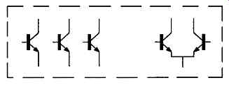
FIG. 44 Multiple individual transistor array Current mirrors
These devices are a specialized application of the facility offered, by simultaneous manufacture on the same semiconductor die, for the production of separate devices having identical electrical characteristics.
In the case of the 'current minor' the function of the circuit is to generate an exit current from one limb of the circuit which is identical to, or bears a constant, fixed, proportional relationship to, the current drawn from another limb. This is a very useful circuit device for many circuit applications, and is widely used in IC operational amplifiers.
The circuits used are normally one or other of the forms shown in FIG. 45, and an appropriate circuit symbol for the general class of these devices is shown in FIG. 46.
Constant current sources
These are basically junction FETs, constructed so that their gate and source electrodes are joined together, and fabricated in a two-terminal package to take ad vantage of the intrinsically high independence of drain current upon drain voltage in FETs. They are available with output currents in the range 0.1 -- 10mA, and with working voltages up to some 50V.
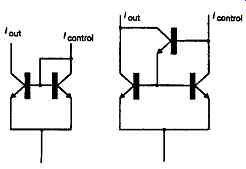
FIG. 45 Typical internal circuitry of current mirrors
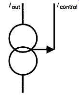
FIG. 46 Circuit symbol for current mirror Instrumentation amplifiers
These are a specific category of IC amplifier intended to offer a very high input impedance, together with a very stable value of gain and DC offset, when used in DC amplifier applications.
These devices will either be straightforward, but high quality, operational amplifiers, in which the circuit design and constructional process has been optimized, with low noise, and high DC and gain stability as the major design requirements, or will be integrated circuit blocks containing the circuit layout shown in FIG. 47. The operation of this type of circuit is considered in greater detail in Section 6.
Other useful characteristics such as a logarithmic relationship between input and output signal voltages may also be offered, in this type of IC, depending on the manufacturer.
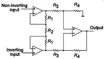
FIG. 47 Internal circuit configuration of instrumentation opamp.
Specialized circuitry
This covers such a wide, and expanding, field that it’s impracticable to discuss it in detail, and the catalogues of IC manufacturers should be consulted to provide detailed information on the available devices. As a rule, such ICs are offered either to allow the use of circuits whose complexity would prevent their satisfactory implementation using discrete components (resistors, capacitors, transistors), such as, for example, the demodulator and stereo decoder circuitry used in FM tuners, or to offer a lower cost alternative to existing circuitry normally implemented with discrete components, as in the RF and AF circuitry of portable radio receivers.
The continuing reduction in the cost of consumer electronics hardware, and its growing incursion into other fields, has only been possible because such specialized circuit blocks have been developed, and, in general, their use has contributed to the reliability of this equipment.
Two cautions should be noted. Of these the first is that special circuit ICs may not be designed to offer as high a standard of performance as the discrete component circuit they are designed to replace, particularly when their main purpose was to allow a reduction in manufacturing costs. Secondly, experience suggests that such special application ICs may be discontinued without warning, as a result of a marketing or sales decision, and this can leave any equipment, in which these ICs have been incorporated, in difficulties in respect of future maintenance. It’s prudent, therefore, to look to see how many directly interchangeable replacements are available for the IC in question, before making a decision to incorporate it into equipment.
Linear uses of digital ICs
The fact that an IC has been designed for use in digital circuitry does not necessarily preclude its use in linear applications, although some sacrifice of linearity or noise figure may have to be accepted in comparison with a comparable IC specifically designed for linear applications. On the other hand, the low cost of such digital ICs, and their availability for use with single 5 V line supplies may make their use very attractive in combined linear/logic circuit designs.
A particularly versatile type of logic device for linear applications is the CMOS inverting amplifier/buffer, which can be self biased into a linear mode of operation using the circuit shown in FIG. 48.
This can either be used as a single stage amplifier, giving a gain in the range 20-50, or, in cascade, as a means of converting a small signal input into a 'logic level' switching waveform.
Low gain amp; Symmetrical squarer circuit
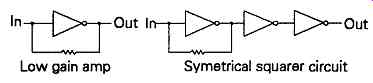
FIG. 48 Linear application of CMOS (digital) inverter stage