AMAZON multi-meters discounts AMAZON oscilloscope discounts
Basic theory
While the mechanism by which a thermionic valve operates is simple to visualize and easy to understand, the way in which 'semiconductor' devices work is much less easy for the would-be engineer to comprehend, and this has, I think, encouraged the 'black box' approach to circuit design, in which the active devices are treated simply as functional blocks, with appropriate connecting wires and well specified operating conditions.
While this way of working may be entirely adequate for logic systems, in which the required output signal is simply a sequence of pulses alternating between 'zero' and 'logic level' potentials, and the restrictions on the supply line voltages, or device currents, may be irrelevant to the operation of the system, it’s too limiting in its constraints to allow much innovative linear circuit design. So, however reluctantly, it’s necessary for the designer of 'solid-state' linear circuitry to have a working knowledge of the characteristics and operating mechanisms of the de vices he wishes to use. Fortunately, it’s possible to possess this understanding at two different levels, which one might call the theoretical and the practical.
I will explain the theoretical basis first, with as few departures from the currently accepted view of theoretical physics as are necessary to avoid undue complexity.
With a few exceptions, the electrical characteristics of all pure solid materials may be classified as belonging to one or other of the three categories of insulator, semiconductor or conductor, depending on their electrical behavior, and this behavior depends principally on the actions of the electrons in the outer orbital shells.
==
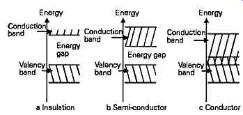
FIG. 1 Electron energy distribution in insulators, semiconductors and conductors
==
Although it’s convenient to visualize the electrons as occupying planetary type orbits around the nucleus of the atom, this is not really a very accurate representation of their status, which is more correctly defined as a series of energy levels. The distribution of electron energies in these three classes of material is illustrated in FIG. 1.
It should be remembered that the electrons in low orbits (close to the nucleus) have the lowest energy level, and those electrons in the outer orbital levels have the highest, so that in order to achieve conduction in insulators or 'undoped' semiconductors some energy input is always required to lift electrons from the outermost normal energy level - known as the 'valency ' level - into that state in which the electrons are no longer tightly bound to the nucleus, known as the 'conduction' level. Between these two energy levels is the so-called 'forbidden' band in which electrons may not reside, unless trapped by impurity atoms within the crystal or crystal defects. The forbidden band, also referred to as the 'energy gap', defines the interval between the maximum energy which an electron can possess, and still be bound to the nucleus by attractive forces, and the minimum energy required for an electron to break free from the atom, and migrate from one atom to another within the crystal.
The outermost normal energy levels of the electrons are called the valency levels, because the electronic distribution within these determines the nature of the physical and chemical relationships between adjacent atoms.
In insulators, even the electrons in the highest nor mal energy states are still very tightly bound to the nucleus of the atom, and the energy gap represented by the forbidden energy levels is wide, so that these valency electrons are not able, except at very high levels of electrical stress, to migrate from these orbital positions into what are termed the 'conduction bands' in which they may move from atom to atom. No electronic current will therefore flow at potentials below those which cause electrical breakdown in the solid.
In conductors, the width of the forbidden band is small, or non-existent, so that the outer orbital levels of the atom (the conduction bands) will be occupied by very many electrons which are loosely bound to the atom and may readily migrate through the solid body, so that electronic current will flow upon the application of a very low accelerating potential.
Those materials within the class known as semiconductors have an atomic structure in which, at temperatures above absolute zero, the thermal energy of the atom may cause some electrons to escape from the tightly bound valency orbits into the more loosely bound conduction band, and this random change of electron orbital position is strongly influenced by the crystal structure in which the semiconductor may exist.
The major class of semiconducting materials of interest to the electronics industry is that in which the atoms have a tetravalent (four electron) outer electron structure, and which crystallize in regular tetrahedral or cubic crystal structures, with the distribution of valency electrons shown in FIG. 2. Such materials will generally be of those elements which occupy group 4B in the periodic table of the elements, of which the relevant section is shown in Table 1, in the order of increasing atomic weight of the elements.
It’s also possible, but with rather greater difficulty in manufacture, to utilize materials, having a similar crystalline and orbital electron structure, formed from compounds of elements in Group 3 with those in Group 5, such as gallium arsenide.
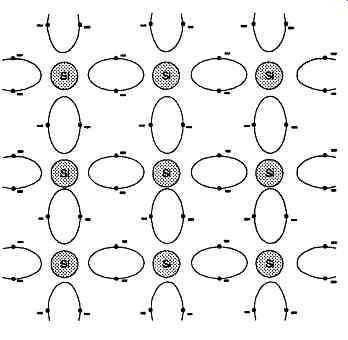
FIG. 2 Regular covalent electron bonding in Group IVB element such as pure
silicon
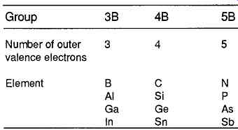
Table 1 Extract from the periodic table of the elements
The effect of doping
Although some of the materials in Group 4B may be of interest in a completely pure chemical form, be cause of the phenomena which may occur at the point of contact between a metallic conductor and the surface of the crystal, the principal applications of semiconductor technology concern the effects which arise at a junction between two similar semi-conducting materials whose electrical characteristics and crystal structure have been modified by the deliberate introduction of small quantities of impurities - a process known as 'doping'. If an element with an outer valence level containing five electrons, such as any of those in Group 5B, is introduced into the otherwise regular crystal structure of a Group 4 substance, the interchange between the outer orbits of the valency electrons shown in FIG. 3 will be disturbed by the presence of the additional orbital electron, and this electron will have a much greater freedom of movement, and can be regarded as occupying a conduction band level.
An impurity atom which has this effect is called a 'donor' atom, and the semiconductor material containing such donor atoms is known as 'N' type, because of its excess of (negatively charged) electrons. Such a 'doped' material will be much more conductive of electricity than the undoped or 'intrinsic' material.
Similarly, if an impurity element having only three outer valence electrons, such as any of those in Group 3B, is introduced into the crystal structure, the disturbance of the shared electron orbits will be such as to leave a vacancy or 'hole' where an electron would otherwise have been, as shown in FIG. 4.
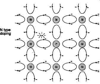
FIG. 3 Disturbance of covalent bond structure in silicon crystal due to
presence of 'donor' type impurity atom
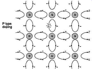
FIG. 4 Disturbance of covalent bond structure in silicon crystal due to
presence of acceptor type impurity atom.
Such an impurity atom is called an 'acceptor' atom, and material doped in this way is known as 'P' type material, because of the presence of the (effectively positively charged) 'holes'. This material is also more highly conductive than the intrinsic (undoped) semi conductor crystal because electrons are able, under the influence of an electric field, to migrate through the material by moving to occupy holes, thereby leaving further holes in the place from whence they had come.
This gives the effect of the holes themselves moving through the material, simulating the action of microscopic particles having an opposite charge to that of the electron. However, because their movement is, in actuality, built up from a large string of sequential movements of electrons moving small distances to occupy adjacent holes, the effective mobility of hole flow in a P type semiconductor is much lower than that of electron flow in an N type material.
For practical reasons, in order to be able to grow crystals whose structure is not too greatly strained by the presence of the impurity atoms, the impurities chosen are generally those of a similar atomic size, such as aluminum or phosphorus for silicon, and gallium or arsenic for germanium, although, in trace quantities, arsenic can be used as an N type dopant in silicon, and indium as a P type one in germanium.
Sometimes the nomenclature 'N-' or 'N+' and 'P-' or 'P+' is used in explanatory diagrams of semiconductor devices to denote materials having a lesser or greater degree of doping than the standard N or P material.
The semiconductor junction and the junction diode
The currently accepted theoretical model of the energy structure within a multi-electron atom is that proposed by the Italian physicist Enrico Fermi, and, because of this, the notional 'average' electron energy level in such an atom is known as the 'Fermi level', or the 'Fermi energy' (Ef). This concept is of importance at the region of contact between dissimilar materials, and particularly so in the case of junctions in semiconductor materials.
In an 'intrinsic' (undoped) semiconductor material, at a temperature of absolute zero, (0°K), the energy distribution of the electrons will be as shown in FIG. 5a, in which the maximum energy level of any of the electrons will be that of the valence band. If the material is at a higher temperature, say room temperature (300°K), the thermal energy of the electrons, even in an intrinsic semiconductor, will allow some of them to escape from the pull of the nucleus, and attain energy levels appropriate to that of the conduction bands, causing the Fermi level to lie between the conduction and valence levels, as shown in FIG. 5b.
Where the material is of N type doping, in which the impurity material has led to an excess of electrons, there will also be electrons in the conduction bands - in addition to those present solely due to thermal excitation - simply because they have been excluded from their normal valence position because of the effects of the crystal structure on the inter-atomic relationships, as shown in FIG. 3. This leads to an electron energy distribution, even at low temperatures, which is more like that shown in FIG. 5b.
On the other hand, if the material is of P type, with an orbital electron distribution of the type shown in FIG. 4, then very few electrons, escaping from the valency levels, will survive being trapped by holes and arrive in the mobile conduction band zone, so that the energy distribution will be more akin to that shown in FIG. 5a. Because of this, the average electron energy level (Ef) in a P type material will be lower than that in an N type, simply because fewer electrons will normally be found in the higher energy conduction bands. The effect of this is that when an N region and a P region are brought into contact, the reciprocal flow of electrons at different energy levels across the junction, due to thermal agitation, will bring the Fermi levels on the two sides of the junction into an energy equivalence, and this will have the effect of displacing the relative energies of the conduction bands of the P and the N type materials. For this reason, electrons cannot flow from the N to the P side of the junction without some external source of energy, and this leads to what is termed a 'potential barrier' (Et>) , between the two zones. Forward conduction won’t occur until the applied potential exceeds this value.
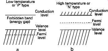
Fig. 5 Average electron energy levels in
semi conductors as a function of temperature or doping level.
Increasing the temperature of the material will increase the thermal energy of the electrons, and will increase the proportion which have sufficient energy to make the transition from valence level to conduction level, even in P type materials where there would normally be few conduction band electrons. This will have the effect of displacing the Fermi energy to a higher level, particularly in the P regions, and this will reduce the potential barrier presented by the junction.
The actual potential barrier will therefore depend both on the nature of the material and on the tempera ture of the junction. For germanium junctions at room temperature (20° C) this is about 0.15V, while for silicon junctions it’s of the order of 0.58V. (Note that the diagrams of FIGs. 5 and 6 relate to electron energy, and so have a polarity sense which is opposite to the normal convention of +ve at the top.)
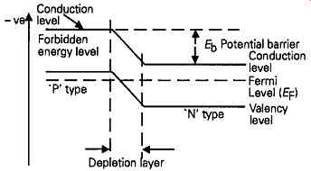
FIG. 6 Mechanism by which potential barrier arises at P-N junction
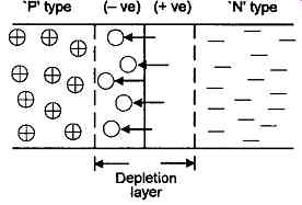
FIG. 7 Growth of depletion layer on either side of a P-N junction
The depletion zone
There is a further important, and related, phenomenon in P-N junctions which is that a depletion zone will arise on either side of the junction, as shown symbolically in FIG. 7. This is an additional effect of the migration of electrons across the junction from the N type (electron surplus) into the P type (electron deficient) regions of the semiconductor, in that electrons which diffuse into the adjacent P type region will occupy the holes which are characteristic of this material.
The effect of this migration is therefore to remove both electrons and holes from a band on either side of the junction, and leave a region which is effectively depleted of available current carriers. However, the loss of an electron from an atom -- even if it has more than will fit into the shared orbital electron structure of the crystal -- will leave a positively charged ion on the N type side of the junction. Conversely, the filling of a hole on the P type side of the junction will also create a negatively charged ion in this region, and the accumulating potential of these V and '- ' charges will eventually shut of f further electron migration across the junction.
In the absence of any externally applied voltage across the junction, the thickness of the depletion layer will depend on the population density, 'e' (epsilon), of free electrons or holes within the junction materials, and also on the size of the potential gap arising at the junction (which in turn depends on the nature of the materials in contact), in that this will determine the extent to which a potential difference across the junction can arise before electronic migration is cut off.
Therefore, due to this movement of electrons, even in the case of a junction with no externally applied potential, there will be an effective potential gradient across the depletion zone, which will be +ve on the N doped side of the junction, and -ve on the P doped side.
However, if an external potential is applied, the effect of the additional electrostatic force field on the electrons and holes will either widen the depletion zone - if a reverse bias is applied, as shown in FIG. 8a - or make it more narrow - if a forward bias is applied, as shown in FIG. 8c, by comparison with the width, in the absence of any applied potential, as shown in FIG. 8b. When a sufficient forward bias is applied to overcome the inherent potential barrier at the junction, the depletion zone will vanish and a current will flow, as shown in FIG. 8d. This gives rise to the type of forward and reverse current flow effects shown in FIG. 9a. Because of the differences in their electron energy characteristics, and in the size of their potential barriers, different semiconductor materials will have dissimilar forward and reverse conduction characteristics, as shown in the diagram for silicon and germanium P-N junctions.
====
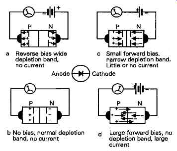
FIG. 8 Influence of external potential on width of depletion zone injunction
'diode'.
a Reverse bias wide depletion band, no current
c Small forward bias, narrow depletion band. Little or no current
b No bias, normal depletion
d Large forward bias, no band, no current depletion band, large current