AMAZON multi-meters discounts AMAZON oscilloscope discounts
Reverse breakdown effects
Ideally, there would be no current flow in the reverse direction until the junction breakdown voltage was attained, nor would there be any forward conduction until the voltage defined by the potential barrier was reached. However, in practice, due to crystal imperfections and residual contaminants, there will always be some small leakage current at low applied potentials, as shown in the expanded view of the region around the origin of the graph, FIG. 9b.
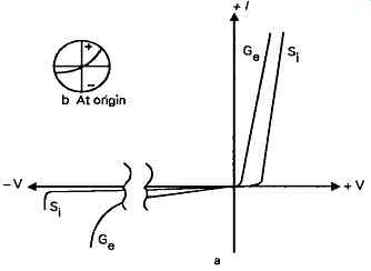
FIG. 9 Normal forward and reverse characteristics of silicon and germanium, junction
diodes.
There will also be an increasing reverse leakage current, at increasing reverse voltages, due both to contaminants and imperfections, and also to ionization of the semiconductor due to electrostatic stress effects, related to the geometry of the device. This last effect is very important in high voltage semiconductor rectifiers.
If the reverse voltage applied across the junction is high enough, the thermal dissipation in the junction, due to the small reverse current flow, may be high enough to increase the leakage current still further, so once some critical reverse voltage is reached, the reverse leakage current will begin to increase rapidly.
In addition, the population density of carriers within a semiconductor depends on the doping level of the materials, so that junctions between highly doped materials will give rise to thin depletion zones, while those between lightly doped materials will have relatively wide ones. This has the effect of modifying the gradient of the P-N junction energy diagram of FIG. 7, as is shown in FIGs. 10a and 10b. This has two practical consequences in very highly doped materials, of which the first is that if the boundaries of the N and P regions become too close together, and the energy levels which elections can occupy are the same on both sides of the depletion layer, the electrons may 'tunnel' in both forward and reverse directions through the depletion layer, at very low applied potentials, in spite of the apparent existence of a substantial potential barrier.
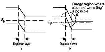
FIG. 10 Effect of doping on potential gradient across P-N junction.
This effect is employed in the manufacture of 'tunnel diodes' , which have the characteristic voltage/current characteristic shown in FIG. 11a, where there is very little forward or reverse voltage drop across the junction. The downward kink in the conduction curve is due to the fact that if a forward bias is applied, this will have the effect of displacing the possible electron energy levels, and preventing further tunneling, which can only occur if the electron can cross the junction without gain or loss of energy.
This causes the forward current to drop once more, up to the voltage at which normal forward conduction resumes.
====
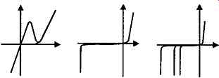
FIG. 11 Forward pulse characteristics of tunnel, zener, and avalanche diode.
a Tunnel diode; b Zener diode; c Avalanche diode
===
The same mechanism is used in ‘zener’ diodes, whose forward and reverse conduction characteristics are shown in FIG. 11b, except that the doping levels are arranged so that electron tunneling does not take place until a few volts of reverse junction potential is applied. The energy distributions across the junction boundary at zero, and at breakdown potentials, are shown in FIGs. 12a and 12b. Typical zener diode reverse voltage breakdown potentials lie in the range 2.5-5V.
===
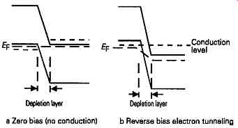
FIG. 12 Fermi levels and conductor 'mechanisms' in zener diodes. Note: Depletion
layer
a. Zero bias (no conduction)
b. Reverse bias electron tunneling
===
The second effect is that in highly doped junctions, the increase in width of the (very thin) depletion layer as a reverse potential is applied won’t be adequate to prevent an electrical breakdown of this layer once the kinetic energy of any leakage electrons, accelerated by the applied field and colliding with other atoms, is sufficient to cause an avalanche of ionization in the material. This mechanism gives rise to the abrupt low-voltage breakdown diodes also commonly, but incorrectly, known as zener diodes, but more correctly termed 'avalanche' diodes. These will be found usually in reverse breakdown voltage ratings from 5-100V. The type of forward/reverse conduction characteristics of these diode types are shown in FIG. 11c. Because of the predictable reverse breakdown potentials, both avalanche and zener diodes form useful voltage reference components.
Avalanche mechanisms also give rise to the reduced breakdown voltage of the relatively highly doped emitter-base junction of a normal silicon junction transistor, which is typically only of the order of 5-6 volts.
(It should be noted that the actual distribution of the depletion zone on either side of the junction is not necessarily symmetrical, unless the P and N materials have an identical concentration of donor or acceptor atoms, but will depend on the relative doping levels of the two contacting regions, so that the width of the depletion layer, other things being equal, will be less on the more highly doped and greater on the less highly doped side of the P-N interface.) Although high electrostatic stress levels at the edges of junctions can cause premature breakdown effects, the reverse breakdown voltage of a P-N junction is principally a function of the extent of the doping of the materials, and will be greater in those materials which have a lower concentration of impurities (lightly doped, e.g. N- or P-) than in more heavily doped ones.
On the other hand, the lightly doped materials will have a lower conductivity, so, for a given junction area, there must always be some degree of compromise in the design of semiconductor rectifiers between conductivity and breakdown voltage.
Junction capacitance
An important inherent characteristic of a non-conducting (e.g. reverse biased) P-N junction is that there will be a significant capacitance between the two halves of the junction, and this will depend on their area and the thickness of the depletion layer by which they are separated. If the bias is low, or the dopant level is high, this depletion zone will be thin, and the junction capacitance will be high.
If, on the other hand, the reverse voltage is increased the depletion zone will widen and the junction capacitance will decrease, and this allows the construction of voltage controlled variable capacitance diodes, which can be made in forms which offer a wide range of initial capacitances, typically from 3-300pF, de pending on the junction area and doping levels used, and with a variety of voltage/capacitance characteristics.
The junction capacitance of a reverse biased diode is approximately defined by the relationship:
C ~w~<V (1 )
…where C is the junction capacitance, e is the mean population density of holes and electrons on either side of the depletion zone, and depends on the doping level, A is the junction area, w is the width of the depletion region, and V is the (reverse) voltage applied across the junction.
To summarize the practical aspects of semiconductor action, certain elements within the chemical group 4B will, when in crystal form, show electrical characteristics which are intermediate between insulators and conductors, and the normally low conductivity of these materials may be increased by doping them with certain types of impurities. Depending on the type of impurity present, this will cause them to have an excess of electrons, (N type), or conversely a deficiency of electrons (P type) giving rise to holes where these electrons should normally have occurred.
When a junction is formed between an N type and a P type semiconductor, electronic current can normally flow only in one direction, from the N type region to the P type one, but only when a sufficient voltage is applied in the forward direction, and the size of this voltage will depend on the junction temperature and on the materials from which the junction is formed.
The conductivity of semiconductor materials is in creased by increasing the concentration of the doping impurity, but this also reduces the reverse breakdown voltage of the junction.
Although it’s convenient to visualize the carriers in P type materials as mobile holes, having the same characteristics as electrons but with a +ve rather than a -ve charge, in reality, the movement of a hole is due to the movement of a sequence of electrons, each leaving a hole behind when it move to fill another adjacent hole. For this reason, while the movement of holes, in response to an applied electric field, appears to be that of small positively charged bodies, the actual speed of movement of holes is much lower than that of electrons.
Majority and minority carriers:
A P type material is defined as a material having a population of acceptor atoms, and an N type one as one with a population of donor ones. However, be cause of crystal structure irregularities or unwanted impurities, some free electrons will always be present in a P type material, and some holes will always occur in an N type one, especially during the passage of current through the junction.
These 'alien' bodies will be less effective as current carriers than either electrons in an N type or holes in a P type, because of their proneness to recombination with the principal carriers within the material. They are therefore termed 'minority' carriers to distinguish them from the holes in a P type or electrons in an N type material, which are known as 'majority' carriers.
Ohmic contacts In order to convert a piece of semiconductor material containing one or more P-N junctions into a practical component, wires must be attached to it. If such wires are simply placed in contact with the material, rectifying action will probably occur, so the method of making such a contact must be chosen so that this does not occur.
A common method is to arrange that the material is very highly doped at the point of contact, with a dopant material which gives the same effect as that already present: For example, a 4 P++' layer on a normally P type material, or an 'N++' layer on an N region. A thin layer of metal, such as gold or aluminum, which would cause a similar type of doping action, can then be evaporated on to the surface of the semiconductor material to form a contact pad.
An even easier method is simply to rely on the fact that even when an element such as aluminum is applied, say, to an N type silicon substrate, on which the aluminum will cause the formation of a P type region - because Al is a donor type impurity - the depletion region of such a P-N junction will be so thin that electrons can tunnel through at very small potential differences. So, for all practical purposes, such a junction is also a non-rectifying one.
Point contact devices
Although nearly all modern semiconductor technology is based on the use of inter-crystalline junctions, it’s worth remembering that, historically, the first application of solid state electronics was in the 'crystal and cat's whisker' point contact diode, based on the use of a thin metal wire pressed into contact with the surface of a piece of crystalline semiconducting material, most commonly galena (lead sulphide), but including other substances, such as household coke, at the whim of the experimenter.
Such metal/semiconductor rectifiers were usable at the input signal frequencies of early radio transmissions and, in the early days of radio, allowed the construction of simple home built receivers. However, devices of this kind were very fragile and uncertain in operation, because of the proneness of the wire contact to become dislodged from the surface of the crystal.
With the advent of VHF and UHF 'radar' systems in World War 2, there was a need for a rectifier diode, for frequency changer applications, which would operate beyond 500MHz. Thermionic diodes became increasingly inefficient as the operating frequency was increased, and were of little value at these frequencies.
Use was therefore made of an updated version of the original 'crystal and cat's whisker' system, but using a small slice of monocrystalline silicon as the crystal, and with a tungsten whisker held in firm contact with its surface. This type of point-contact diode was subsequently supplemented by similar diodes based on germanium, of which the lower melting point facilitated the production of larger lumps of single crystal material. In manufacture, it’s customary to pass a brief pulse of high current through the diode which will 'spot weld' the wire contact - which will generally be either of tungsten or of gold - onto the surface of the crystal, which makes the whole structure physically robust.
Silicon point contact diodes have a higher forward voltage drop (typically 0.3 - 0.45V) than germanium ones (which will typically be in the range 0.1 - 0.2V), but have a better high frequency characteristic, and remain usable up to the GHz range, whereas the germanium diode loses efficiency above some 50 100MHz.
Because of the high electrostatic stresses which arise at a point, the reverse breakdown voltages in point-contact diodes will always be relatively low, in the range 5 - 15 V.
Germanium point contact diodes are still commercially available, and find use in relatively low frequency applications where their low forward con ducting voltage drop is of advantage. They do, however, have a relatively low reverse resistance and reverse breakdown voltage in comparison with the silicon junction devices, which are now by far the most common commercial type.
A useful, and now, happily, almost universal convention is that the cathode (N type region) of a rectifier diode will always be marked on its case with a black band or ring. As a mnemonic, if the end of the diode marked with a black ring is connected to the negative end of a battery, current will flow.
The point contact transistor
Theoretical studies of the action of the metal/semiconductor rectifier had led to the concept of a depletion zone within the semiconductor material in proximity to the metal contact, which would lead to a modification of the distribution of carriers as shown for a point metallic contact on a P doped substrate (base) in FIG. 13a.
The idea of introducing a further metallic point contact into this depletion zone, so that electrons emitted by this contact would be collected by the other positively charged wire, instead of disappearing into the P type base, was conceived, in December 1947, by John Bardeen and Walter Brattain, at the Bell Tele phone Laboratories, in the USA, using the structure illustrated in FIG. 13b.
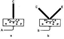
FIG. 13 Point contact diode and point contact transistor
The major practical problem, that of maintaining the two contacts sufficiently close together to allow effective collection of the emitted electrons was solved by Bardeen and Brattain, in their first successful experimental model, by the use of a ' V shaped wedge of polystyrene, which had been coated on its angled faces with a thin film of metallic gold. The continuity between the two faces was then broken at the apex of the ' V by cutting off the tip of the wedge.
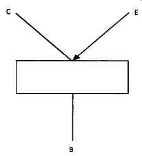 FIG. 14 Symbol for PNP transistor - derived from structure of early experimental
model.
FIG. 14 Symbol for PNP transistor - derived from structure of early experimental
model.
While this early experiment is of little practical importance, apart from establishing the feasibility of such a device, it has given both the 'emitter', 'base' and 'collector' terminology to the transistor, and also the graphic symbol which is now used to represent the device, as shown in FIG. 14 -- in spite of the fact that the physical structure of contemporary transistors is a long way removed from this layout.
In early point-contact transistors, the only practical method of operation was to inject a current into the low impedance emitter circuit, so that a substantially identical current could be drawn from the collector.
Amplification was possible because the output impedance, at 10,000-20,000 ohms, was very much greater than the input impedance, which might be typically in the range 25-200 ohms.
Because of the possibility of voltage gain arising from this characteristic, the term 'transfer resistor' or 'transistor' was coined.
While, ideally, the collector current would be identical to that of the emitter, too great a spacing between emitter and collector points would reduce this figure, while any ionization due to the electrostatic stress at the collector point might even increase the current transfer ratio to rather greater than unity.
All in all, the point contact transistor was never much more than a laboratory curiosity, since its mechanical fragility and the general unpredictability of its electrical characteristics made it a difficult component to use. However, the possibility of achieving the required proximity between collector and emitter regions, by diffusion of suitable impurities within the crystal body, allowed the construction of fully usable and reliable components.
The bipolar junction transistor
In the previous sections we have considered the nature of the semiconductor P-N junction, and the way in which such a P-N junction can be used to make a robust solid state rectifier diode. While such semiconductor diodes are valuable components, in that they are much more compact, much more efficient and simple to use than the thermionic equivalents, and have both greater reliability and much greater life expectancy, it’s the fact that this mechanism can also be used - in various different arrangements - to make an amplifying device which has caused semiconductor technology to have such an enormous impact on the electronics field.
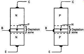
FIG. 15 Single crystal junction transistor structures. Note: Depletion zone
The normal 'bipolar' junction transistor is made by combining a pair of P-N junctions, so as to form a composite three-segment N-P-N or P-N-P element, within a single crystal block, to which connecting wires are attached by 'ohmic' (i.e. non-rectifying) contacts, in the manner which is shown schematically in FIG. 15. Because of the way in which these regions of the semiconductor material operate when the device is used, the upper section is called the 'collector', the central one the 'base', and the lower one the 'emitter'. For practical reasons, the P type base region in the NPN slice - or the N type base region in the PNP one - will have a relatively low impurity level, as will the collector region. The emitter region will have a relatively high doping level.
As explained above, when a P-N junction is formed within a single crystal block a depletion band arises on either side of the junction, in which all the normal carriers are removed by recombination as a result of electron diffusion across the junction. In the case of a thin, lightly doped, base layer, sandwiched between two oppositely doped regions, the whole of the base region will be depleted of carriers. Therefore, when the collector-base junction is reverse biased, as shown in FIG. 16, no significant amount of current will flow from the base region to the collector at any potential below the collector-base junction reverse breakdown voltage. If, on the other hand, the switch Si is closed, forward biasing the emitter-base junction, a substantial flow of electrons will pass from the emitter into the base region, and, since this region is almost entirely depleted of carriers, these electrons will be swept up by the accelerating effect of the base-collector electrostatic field.
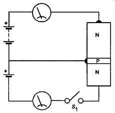
FIG. 16
The only loss of emitter current on its way to the collector will be due to recombination with the residual holes present in the base, and provided that the base region is thin (of small volume) and lightly doped, this loss will be small.
The same circuit can be rearranged as shown in FIG. 17, when similar considerations will apply, in that when S2 connects the base region to the emitter there will be no current flow from the emitter to the base, so that the only collector current will be that due to the reverse leakage current of the base-collector junction.
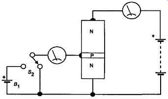
FIG. 17
If, however, S2 connects the base to the battery B1, the emitter-base junction will now be forward biased, and virtually the whole emitter current will be swept up by the collector. The only base current which will flow into Bi will be due to those parts within the base region where the accelerating base-emitter field is locally stronger than the collector-emitter one. The internal layout of modern junction transistors is chosen to minimize this.
The base current flow therefore effectively controls the emitter collector current flow, and the ratio of the collector to base currents is known as the (common emitter) 'current gain', and denoted by the Greek symbol 'beta'. This can have a value in the range 15-50, for high-current power transistors, to 100-1000 for low current 'small signal' devices. The less commonly specified ratio of collector to emitter current, as would be found in the circuit layout of FIG. 16, is denoted by the Greek symbol 'alpha'. Since the emitter current in a transistor is the sum of the base and collector currents, the relationship between these two ratios can be derived, and is:
Although the example of an NPN transistor has been chosen to explain junction transistor action, the same arguments will apply equally to a PNP one if the applied potentials are reversed in polarity and the action of 'holes' is substituted for that of electrons.
Modern manufacturing techniques allow the production of PNP transistors which are substantially identical, in their current gain and other characteristics, to NPN ones. However, because the motion of holes is slower than that of electrons, PNP transistors, in which the P regions are relatively thick, are slower in response speed than the NPN ones where the only P region is the very narrow base section.
The collector-base breakdown characteristics of PNP type silicon junction transistors are also worse than NPN ones, due, at least in part, to the differences in the effectiveness of the technology available for producing N doped silicon, as compared with P doped material, so that high voltage silicon transistors will almost invariably be NPN ones.
The converse is true for germanium devices, where the performance of PNP devices is superior to that of the NPN ones. Because of their inferior reverse leak age characteristics, due mainly to their lower maximum operating temperature, germanium devices have now been supplanted almost completely by those based on silicon.
Moreover, because manufacturing skills and techniques depend on research, and, for commercial reasons, this is mainly devoted to those aspects of the business which offer the greatest market return, a very substantial gulf in manufacturing and applications technology now exists between germanium and silicon materials, and this disparity is entirely in favor of silicon based components. The semiconductor circuit designs, and related comments, offered in this guide will therefore apply to silicon based devices, unless otherwise stated.
To summarize, in a P-N junction, electronic current can flow easily from an N type (electron surplus) region into a P type (electron deficient) one, provided that the forward potential is enough to overcome the potential barrier which will exist at the junction. This potential barrier will depend on the nature of the materials forming the junction, on the junction temperature, and, to a lesser extent, on the doping levels used.
Electronic current won’t flow from a P type junction to an N type one, at potentials below those high enough to cause reverse junction breakdown, apart from a leakage current mainly due to minority carriers, and this leakage current is strongly dependent on junction temperature, reverse junction potential, impurity (doping) level and the presence of defects in the crystal structure.
If, however, within a single crystal body, two PN junctions are formed to make an NPN or PNP three layer sandwich, and if the outer regions of this sandwich are sufficiently close together that the depletion zones which will arise in the central layer can overlap, then electrons (or holes) drawn into the intermediate region (known as the base) from a forward biased one (known as the emitter) can readily cross this depleted base region, without loss due to recombination.
If the other P-N junction is reverse biased with respect to the base, this means that it will have a forward bias in respect to any electrons or holes injected by the emitter, so that these current carriers (electrons or holes) will be swept up by the accelerating potential present on the third (or collector) region in this NPN or PNP sandwich.
In practice, this allows a relatively small current injected into, or drawn from, the base region, at a relatively low potential - of the order of 0.5- 0.6V - to control a much larger current at a much higher collector potential, and this allows a large degree of signal amplification.
The current gain or beta of such a three-layer device, known as a junction or bipolar transistor, will depend on the thinness of the base region, as will the high frequency response, since it will take a finite time for an electron or hole to cross the base region.
The maximum operating voltage at which such a transistor may be used will also depend on the width of the base layer, and will increase as the base region thickness is increased. For this reason, high levels of current gain, or good high frequency response characteristics, are more readily obtained in transistors intended to operate at relatively low collector voltage levels.