AMAZON multi-meters discounts AMAZON oscilloscope discounts
(cont from part 1)
Phase-splitter systems:
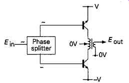
The need arises quite frequently to convert a single alternating input signal into a pair of identical 'mirror image' waveforms, as illustrated in FIG31, per haps for driving a so-called 'push-pull' amplifier stage, as shown, schematically, in FIG32, where a pair of transistors are driven with opposed signal voltages so that their outputs will combine to give a symmetrical drive.
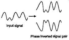
FIG31 Phase Inverted signal pair
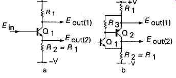
Since Q1 is acting as an emitter follower, with unity gain, the voltage gains of this system will be very nearly +1 and-1. Also, since Q1 is an emitter follower, the circuit can be elaborated by the use of any one of the improved forms shown in FIG25, as For example, as shown in FIG33b.
While this arrangement would be quite satisfactory for AC coupled systems, in which there were DC blocking capacitors in the two output limbs to avoid problems due to the dissimilar DC potentials at the two output points, it would be inconvenient for use in DC amplifying circuits.
An alternative arrangement which is sometimes used, in spite of its lack of elegance in design, is that shown (neglecting DC potentials) in FIG34a, where a second amplifier stage, Q2, is added simply to invert the phase of the output signal at Q2 collector, and the degree of signal attenuation introduced by the potential divider R2/^3 is chosen to remove the additional gain provided by Q2. This does, however, allow the two output signals to be delivered at the same static DC level.
A greatly improved form of this circuit, known as a 'floating paraphase', is shown -- again neglecting DC coupling potentials -- in FIG34b. In this, the resistors R2/R3 are part of a negative feedback network which will allow the output signal voltages from Q1 and Q2 to be maintained accurately equal, though in.
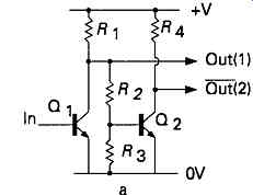
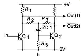
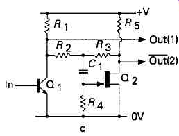
FIG34 Phase-splitter circuit arrangements antiphase, over a wide frequency
range, and independently of variations in the gain of Q2. The difficulty
with this circuit, in DC operation, lies in the provision of a proper DC
bias for Q2, though a zener diode between the junctions of R2 and R3 and
Q2 base could provide a somewhat restricted answer. For circuits using thermionic
valves, or various field effect devices, intended for use only in AC systems,
the use of a DC blocking capacitor, C1, illustrated, in the case of a junction
FET, in FIG34c, provides a very satisfactory answer to this problem.
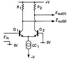
However, by far the best answer to this requirement is the use of a long-tailed pair circuit, shown in FIG35, where, if Q1 and Q2 are matched in their characteristics, and the common emitter circuit resistance, shown in FIG15a, is replaced by a constant cur rent source having a high dynamic impedance, the two output potentials will remain closely similar over a very wide frequency (and temperature) range.
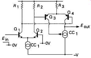
If more amplification is required, the input long tailed pair can be followed by a further pair, Q3 and Q4, as shown in FIG36. If the two push-pull outputs are then recombined by a current mirror, this layout forms very linear symmetrical high gain amplifier stage, an arrangement which has formed the basic gain stage in both operational amplifier, and high quality audio amplifier circuitry.
Other small-signal junction transistors:
The designs shown above have been intended, almost exclusively, for use with silicon planar transistors, because these are by far the most commonly found in practice, and are, generally, the least expensive in cost.
There are, however, other junction semiconductor types based on germanium and gallium arsenide- the latter being an artificial type of semiconductor made, expensively, by the co-crystallization of a trivalent element, gallium, with a pentavalent one, arsenic, a so-called 3-5 semiconductor -- which have uses in specific applications. Of these, germanium junction transistors are currently made by similar manufacturing techniques to those used for silicon devices, and differ from them, principally, in having higher leakage currents and lower maximum working temperatures, which leads, in turn, to lower permissible power dissipations for any given 'chip' size. They do, however, have a lower 'turn-on' point in their base voltage/collector current curve, as shown in FIG37, and this can be useful in circuitry for which the available supply voltage is limited. In general, though, they represent an obsolescent area of semiconductor technology.
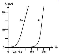
FIG37 Conduction characteristics of silicon and germanium transistors.
This is far from being the case with gallium arsenide, which has, in several ways, superior performance to silicon -- for example, lower noise and a higher possible operating frequency, due to the greater electron mobility within the crystal lattice -- but limited in use by the higher material cost. Its principal application, to date, is in the manufacture of VHF (micro wave) field effect transistors, operational up to beyond 12GHz.
Bipolar junction power transistors:
These, also, are mainly made from silicon, though some germanium types are still available. They are, in essence, substantially identical to small signal device s, except that the method of construction is specifically adapted to allow high working voltages as well as large collector/emitter currents and power dissipations.
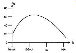
The penalty incurred by the use of the larger junction areas, and greater junction thicknesses, required for this type of use, is that the current gain will usually be much less than that of small-signal junction transistors, and will be more strongly dependent on collector current, as shown in FIG38. Because, as shown in equation (1), the mutual conductance, gm of a bipolar transistor depends on its collector current, power transistors can offer very high values of gm indeed, up to 200 Siemens (A/V). Also, because for low input impedances, the output impedance of a simple emitter follower, of the type shown in FIG24, approximates to i/gm ohms, very low output impedances can be provided by power transistors, when operated at large quiescent currents.
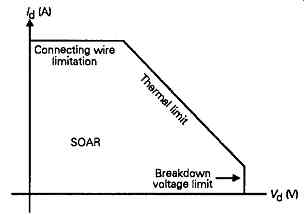
There is a restriction in the use of silicon junction power transistors in respect of the permissible collector current which may pass for any given value of collector voltage. This then leads to the need to define usable operating conditions, referred to as the 'safe operating area rating' (SOAR). This problem arises from the fact that, owing to the large emitter junction areas necessary to permit high collector currents, the thermal conductivity across the junction may not be high enough to ensure that the whole area of the junction will always be at the same temperature.
Also, because of manufacturing imperfections, there are likely to be some variations in junction thickness and dopant concentration across this junction, so there is a probability that the current flow through the transistor, even if the junction temperature is constant across its width, won’t be uniformly distributed across this junction. This means that, in use, some small areas of the base/emitter junction may become hotter than others, and since the current flow for a given base voltage will increase as the junction temperature increases, this can lead to a situation in which current will tend to flow increasingly through these areas of the junction -- which will cause these regions to get still hotter, so that more current will tend to flow through them, and so on. In the absence of any external restriction on the collector current flow, this effect could result in a destructively high current through some small region or regions of the junction, a condition known as 'thermal runaway'. To avoid this problem, the manufacturers of power transistors publish safe operating area curves, which define safe values of collector current at specified values of collector voltage, of the kind shown in FIG39. In this, that part of the graph between points ' A' and ? ' relates simply to the maximum current which can be carried by the wires used for the internal connections to the transistor before these wires fuse. The part between points 'B' and *C defines the maximum thermal dissipation of the transistor, (the simple pro duct of current and voltage) when the transistor mounting pad is held at a fixed temperature, usually 20°C.
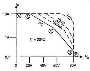
FIG39 Safe operating area rating (SOAR) for typical power transistor.
It should be noted that this quoted value is usually unrealistically high, since even the best transistor heat sinks won’t keep the transistor at room temperature, so it’s wise not to approach this value too closely in practical designs.
That portion of the curve between points 'C and 'D' indicates the area of likely thermal runaway, if either the current or voltage levels are exceeded. Finally, the portion between points 'D' and ?' simply defines the value of collector/emitter reverse breakdown voltage of the transistor at relatively low current and dissipation values.
The actual boundaries of the thermal limits and the secondary breakdown threshold are time dependent, because of the thermal inertia of the junction, so an 'overrun', if of very short duration, and not repeated at too high a rate, won’t necessarily lead to device failure.
It should also be noted that the actual voltage at which this breakdown will occur, for any transistor, will depend on the base/emitter circuit conditions, in that the collector/base breakdown voltage, ???, at zero collector current, particularly when the base/emitter junction is reverse biased, is greater than the collector/emitter breakdown voltage, Vceo, at zero base bias. In addition, the value for Vceo will depend on the base/emitter circuit resistance, and will be higher for low values of base/emitter external resistance.
In general, for reliable operation, the designer should ensure that the operating conditions of the transistor keep well within the SOAR curve.
Improvements in manufacturing technology, principally in respect of the purity of material and uniformity of thickness of the junctions, and in keeping the total thickness of the ‘die' (the tiny slice of single crystal semiconductor on which the diffused regions are formed) as small as possible consistent with its required operating voltage -- so that proximity to the thermally conductive 'header' will hold the junction temperature more uniform -- mean that recent designs of power transistor will tend to have a better performance, and may be more reliable under arduous operating conditions.
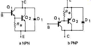
FIG40 Monolithic Darlington transistor construction
So, in the case of US 'JAN' 2N.', and the Japanese '2SK/2SA' series devices, as well as for the European Tro- Electron' *BD...' type nomenclature, the higher type numbers may indicate improved designs.
A widely available form of power transistor is the so-called Darlington device, in which an input transistor, Q1, is fabricated, as an emitter follower driver stage, on the same silicon chip as the power transistor, Q2, as shown in FIGs 40a and 40b, for the NPN and PNP versions. These devices are widely used in hi-fi audio amplifiers, and the 'economies of scale' therefore means that they are relatively inexpensive for their operating voltage and power ratings.
Darlington output transistors offer very high values of current gain, up to, say, 2500, which means that they require relatively low values of input drive current for full output. As output transistor pairs in push-pull Hi-Fi amplifiers they suffer from the small drawback that, since the driver transistor is on the same chip as the power device, it will also heat up at the same time, which makes maintaining the correct value of forward bias for the transistor pair- which will, of course, alter with chip temperature -- somewhat more difficult.
Circuit characteristics of Field effect devices
Junction field effect transistors (FETs)
General characteristics
The construction of these transistors was discussed in Section 5, but, in general, they rely on the fact that any P-N junction, especially if reverse biased, will generate a depletion zone (a region denuded of current carriers) on either side of the junction, and that this depletion zone can be widened by increasing the reverse bias on the junction, or narrowed by reducing the bias, to provide a means for controlling current flow through any semiconductor region in proximity to this junction. This action is illustrated, schematically, for an N-channel FET, in FIG41. Although this summary of the method of operation of an FET, and the circuit applications which I have shown, refer to N-channel devices, (i.e. those in which the conducting channel is an N type material, and the gate electrodes are P type), the method of operation and the circuitry shown, will apply equally to a P-channel FET, except that it could be a little slower in operational speed.
In FIG41a, a thin strip of N type semiconductor has been formed with ohmic (ie. non-rectifying) contacts, X and Y at either end, and a pair of P type junctions has been diffused into either side of the strip.
With no negative bias applied to the P junctions, the depletion zones will extend uniformly on either side of the P-N junction leaving a channel through which current can flow from X to Y. If the P type regions are at the same potential as the current source, X and the drain, Y, is then made more positive, the potential drop along the strip of semiconductor material, due to current flow, will reverse bias the gate junction to wards the drain end of the slice, and will cause the boundaries of the depletion regions to become de formed, as shown in FIG41b, restricting the thickness of the open channel through which current carriers can flow.
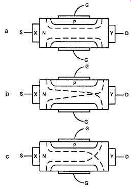
FIG41 Effect of increasing drain voltage on FET with constant source-gate
bias
Finally, when the drain voltage, on Y is high enough, depending on the doping level and thickness of the channel strip, the two depletion zones will meet, which will cut off the free flow of carriers, as shown in Figure 641c. When this happens, there will be no residual potential gradient along the rest of the channel -- all of which, up to the point where the depletion zones join, will be at the same potential with respect to the P type gate region. With normal small-signal junction FETs this effect occurs at a drain voltage of 2-3V, with respect to the source, and, in this condition, the flow of current along the channel is restricted by the ability of the carriers to tunnel through the depleted neck of the channel at the end nearest to the drain: a condition in which the drain current flow is largely independent of the source-drain potential.
This condition is known as pinch-off- a term which should not be confused with cut-off, where the negative gate bias has been increased to the point where all current flow along the channel has been cut off -- and is the normal operating condition for a junction FET, when used as an amplifier.
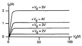
All normal bipolar junction FETs are of depletion type, which is to say that the drain current will be at a maximum value when the gate voltage is zero with respect to the source and will decrease as the gate is made more negative (in the case of an N-channel FET). When operated in the pinch-off condition, the drain current depends almost entirely on the ability of the current carriers -- electrons in the case of an N channel FET -- to tunnel through the depletion zone, and this is largely unaffected by drain voltage. How ever, the breadth of this pinched-off region is still affected by gate bias, giving the characteristic drain current vs drain voltage curves shown in FIG42, for various values of gate voltage.
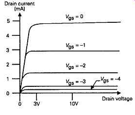
FIG42 Drain current vs. voltage
Circuit applications
Because the drain current is almost completely independent of drain voltage, this gives the junction FET a very high dynamic impedance, as measured at its drain, and also allows the FET to be used as a very simple and efficient 'two- terminal' constant current source, in either of the circuits shown in FIG43, up to the drain/gate breakdown voltage of the device -- usually in the range 25-40V for a small signal FET. In the case of the circuit shown in FIG43a, the output current will be predetermined by the characteristics of the FET; a fact which allows the manufacture of two-terminal constant current sources which can, by suitable choice of channel thickness and doping level, be offered with a range of output currents, usually within the range 02-20mA. The circuit shown in FIG43b is usable with most junction FETs, and allows the current through any given FET to be con trolled by the chosen value of source resistor, RVV which can be adjustable.
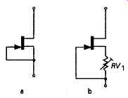
FIG43 FET constant current sources
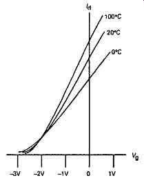
FIG44 influence of temperature on drain current characteristics
The drain current vs. gate voltage relationship of a typical small-signal N-channel junction FET is shown in FIG44. Because the energy of the carriers is dependent on temperature, and their energy influences the boundaries of the depletion zone, the drain current for any gate voltage is still somewhat temperature dependent. It will be noted also that the usable gate voltage extends only up to some +0.5V, beyond which the gate/channel junction will become just a conducting junction diode, and FET action will cease until the gate is once more reverse biased.
The slope of the Id/Vg curve is governed, for an ideal device, by the relationship where Id is the drain current, I_dss is the drain current at zero gate voltage (gate shorted to source), Vs is the gate-source voltage, and Vgc is the gate (cut-off) volt age for zero drain current.
Although this relationship specifies a curved I/Vg characteristic, it’s still significantly more linear than the comparable base voltage/collector current relationship for a typical silicon junction transistor. How ever, for typical small-signal FETs it’s also much less steep, with gm values of only 2-10mS (mA/V) as compared with, say, 45mS for the bipolar transistor.
This means that a small-signal amplifier stage based on a junction FET will have a lower stage gain, by a factor of some 5-20 times, than the equivalent stage using a bipolar transistor, as can be seen from the relationship:
…where Rx is the load impedance.
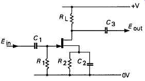
When the FET gate is in a reversed bias condition -- which is that of normal operation -- the gate input impedance is very high indeed, up to a million megohms, and the drain impedance can be as high as 2 megohms. This makes the junction FET very suitable for high impedance circuitry. It’s also a very convenient device for circuit design, since it’s not necessary to derive a specific forward bias for the gate from the supply line (which can lead to problems of unwanted signal breakthrough), instead of which, 'source bias' -- similar to the 'cathode bias' used with thermionic valves -- can be used, as shown in the simple amplifier stage of FIG45. Where the input signal excursions are less than +/- 0.5V p-p, the bias circuit, R2/C2, can even be dispensed with entirely, with suitable FETs.
The junction FET has similar characteristics in use to a low power 'pentode' valve, and will give similar levels of stage gain and distortion, if used at the same supply voltage levels. However, operation at valve type supply voltages is not usually practicable, since junction FETs are mainly limited to drain voltages in the range 15-50V, so with usable values of drain load impedance, the stage gain won’t usually be very high.
'Cascode' operation:
The junction FET can, within the limitations indicated above, be used in almost all the circuit designs shown above for bipolar junction transistors. However, there are some applications where the fact that a small signal FET will operate at a 2-3 V negative gate bias is very convenient, such as the high output impedance cascode circuit shown in FIG46. This layout gives very good isolation between the input and the output circuits, and allows use at radio frequencies without 'neutralization' -- see Section 14. If the gate of Q2 is returned to some positive voltage, rather than the zero volt line, a junction FET can be used in place of Q1, to allow advantage to be taken of the FETs very high input impedance.
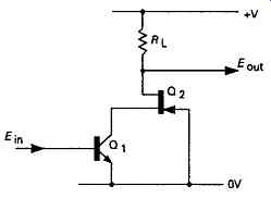
FIG46 Bipolar FET cascode amplifier
The circuit of FIG46 can be adapted, as shown in FIG47, to give an extremely high stage gain, probably in excess of 10,000, by using another junction FET, Q3, as a high impedance load, and then interposing a high input impedance emitter follower circuit, Q4/Q5, between the output of Q2 and the load.
Moreover, because the stage gain is so high, the input signal voltage required by this circuit, even for the maximum possible output voltage swing, is very small, so that the distortion introduced by the curvature of the base voltage characteristics will also be kept to a very low level.
Very similar circuit arrangements, but based on bi polar transistors rather than junction FETs, are avail able in IC form, as, for example, the National Semiconductors LM3900 and LM3301, or the later LM359 IC. This particular device offers a typical gain, at frequencies up to 100kHz, of some 4000, into a 10k/2 load, a very low input noise level, when used as an inverting amplifier, and an HF gain/bandwidth pro duct of up to 400MHz. For reasons noted above, it will also offer a very low level of harmonic distortion.
However, the problem with all circuit arrangements which obtain high stage gain values by the use of very high values of load impedance is that they are dependent on keeping the value of stray capacitance at the collector or drain of the amplifying device to a very low level, which can pose problems in discrete circuit layouts. So, if high gain values are required it’s usually better to use several conventional amplifying stages in cascade than to seek to get it in one go.
MOSFET devices
General characteristics of low power types There is a wide class of semiconductor devices, known variously as insulated gate FETs, or MOSFETs (named after their usual method of construction, met al-oxide-semiconductor FETs), usually based on a slice of very high purity single crystal silicon (though, in some very high frequency devices, gallium arsenide is also used), which rely on the ability of a potential applied to a gate electrode to electrostatically induce negative or positive electric charges, electrons or holes, in an otherwise non-conducting semiconductor layer.
Historically, this was one of the earliest forms of semiconductor device whose manufacture was at tempted, and is illustrated schematically in FIG48. In this, a strip of some semiconductor material having a very low impurity level, and therefore having a very low level of intrinsic conductivity, is formed with two more highly doped regions (the source and drain electrodes), diffused into it -- the regions designated N+ in the case of the N-channel MOSFET illustrated. A thin layer of some non-conducting material, usually silicon dioxide or silicon nitride in the case of a silicon substrate, is then formed on its surface. (In practice, (his would normally be done as a first step, and the N+ regions diffused through apertures etched through it). On top of this insulating layer a conducting electrode, the gate, is deposited, whose geometry is chosen so that it overlaps both the source and drain N+ regions. If the insulating layer is very thin, when a positive potential is applied to the gate metalizing a layer of electrons will be formed, by electrostatic induction, under the surface of the insulating layer, in the very low conductivity (P-) material joining the two N+ regions. These electrons are mobile, and will move from source to drain, or vice versa, in response to an applied positive potential, with the vacancies left by their removal being instantaneously replaced by electrostatic induction.
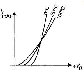
FIG49 Characteristics of enhancement type MOSFET
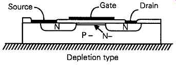
FIG50 Construction of N-channel MOSFETs
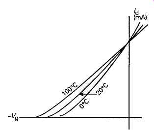
FIG51 Characteristics of depletion-type MOSFET

FIG52 Construction of dual-gate MOSFET
This type of device, in which little or no current will flow from source to drain in the absence of a gate voltage, is described as an N-channel 'enhancement mode' MOSFET, and it will have a gate voltage vs. drain current characteristic of the kind shown in FIG49.
As in the case of junction FETs, 'complementary polarity' MOSFETs (ie, P-channel rather than N-channel) can be made by diffusing highly doped P regions, usually known as P+, into the silicon strip, in place of N+ ones, and these devices will have very similar characteristics, though of opposite working polarity, to the N-channel types.
If, in the case of an N-channel MOSFET, a thin layer of N-doped silicon is formed underneath the gate region by surface diffusion, before the oxide or nitride insulating layer is formed, as shown in FIG50, some source-drain current will flow, even in the absence of an applied gate voltage, to give the kind of gate voltage vs. drain current relationship shown in FIG51. This type of device would be described as an N-channel depletion mode MOSFET, since the residual n-doped conducting layer can be 'depleted' of carriers by the application of a negative gate voltage.
This kind of MOSFET is usually only found in small signal N-channel devices, especially where two separate gate regions are formed, as shown in FIG52, a dual-gate MOSFET, to provide electrostatic screening between gate 1 and the drain, for use in RF applications.
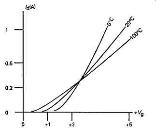
As shown in FIGs 49 and 51, there is a degree of temperature dependence of the drain current for a given gate voltage, though, because these curves intersect, there will be some point on the Jd/Vg curve where the effect of temperature will fall to near zero.
Circuit applications MOSFETs can be used in almost all of the circuit layouts applicable to junction FETs, or even to bipolar junction transistors, with the added advantage that the operating gate voltage range can extend on either side of 0V, up to the level at which the gate/substrate insulation breaks down, when the device is destroyed.
The characteristics of MOSFETs cannot be predicted from any theoretical model, since the relation ship between gate voltage and drain current will depend to a large extent on the thickness and dielectric constant of the gate insulating layer, in relation to which the skill of the manufacturer lies in producing an insulating barrier which is very thin, so that a voltage as low as 2-3V will allow a usable (mobile) charge layer to be induced in the channel, while being able to sustain voltages of the order of 30-40V without breakdown.
However, apart from the minor stray field effects due to errors in the manufacturing geometry, which mainly affect the shape of the /d/V curve at the onset of conduction, the linearity of the 7d/Vg curve is very high, since it’s largely controlled by the physical relationship between applied voltage and induced charge, which is very linear. Also, because of the nearly instantaneous induction of charge in the channel, following on application of a potential to the gate, and the absence of 'hole storage' effects, MOSFETs are extremely fast in operation -- limited mainly by the relatively high gate-source capacitance, which forms a capacitor which must be charged or discharged through the gate/source circuit impedance before the gate-source voltage can increase or decrease. This encourages the use of MOSFETs in RF applications, where they can outperform both bipolar transistors and junction FETs. Otherwise, they can be used in most of the circuits shown above, with the reservation that care must be taken to ensure that the gate-source, or gate drain breakdown voltage is never exceeded, however briefly, or the device will be destroyed.
Power MOSFETs
The high speed and relatively high linearity of the MOSFET transistor encouraged the development of these devices in both higher voltage and higher power forms. The main difficulty in a simple development of the lower power versions arose because in the small signal designs the device is formed in a way which makes the channel parallel to the surface of the chip.
This kind of device would be described as a lateral FET, because the current flow will be from side to side, in contrast to the flow of current through a bipolar junction transistor, which would be vertical, through differently doped semiconductor layers formed one on top of another.
For higher drain currents, the impedance of the channel must be made as low as possible, which entails, among other things, making the channel length as short as possible. In normal lateral FETs the closeness of the two ends of the channel to one another is determined by the skill of the manufacturer in forming and applying photo-resist masks, through which diffusion and etching processes can be carried out.
With the technology available at the time, it was difficult to produce very short channel lengths by this means, so the makers adopted 'V' and U designs, in which the device was manufactured, like a bipolar transistor, with appropriately doped semiconductor layers formed one on top of another, as in a junction transistor, and then V or IF shaped channels were etched into the device, as shown in FIGs 53a and 53b. The exposed surface was then oxidized to form an insulating layer, so that the gate metallization could be applied across the now vertical channel region. In these cases, for manufacturing convenience, the channel would be formed in a very low conductivity layer which had a very small residual P type impurity level, described as P-, giving the equivalent of an NPN junction transistor in which the emitter and base are connected together.
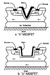
FIG53 a V MOSFET; Drain; b. U' MOSFET
The U MOSFET was somewhat better for high voltage use because the rounded bottom of the groove led to lower levels of unwanted electrostatic stress across the electrically fragile gate insulating layer.
Neither of these types are particularly suited to the manufacture of P-channel MOSFETs, for which the 'T' MOSFET construction is now preferred.
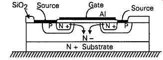
The construction of this kind of device is shown in FIG54, and employs the lateral diffusion of the N+ source regions into preformed P- zones to reduce the resulting effective length of the channel below that which the surface masking alone could easily provide.
As in all power MOSFETs, the possible channel cur-rent flow is increased by constructing a large number of channels, connected in parallel. An elegant design of this type is that introduced by International Rectifier Corp., of the USA, in their 'HEXFET devices, in which the parallel MOSFET regions are fabricated as a series of hexagonal pits, as in a honeycomb, and illustrated in FIG55. This paralleling of the channels also increases the mutual conductance (gm) of the device, so the gm is related, as a function of manufacturing technique, to the total drain current, for any given gate voltage. A typical power MOSFET gate voltage vs drain current relationship is illustrated in FIG56. As with other MOSFETs, the power MOSFET has a negative temperature coefficient of drain current vs gate voltage above a certain drain current value.
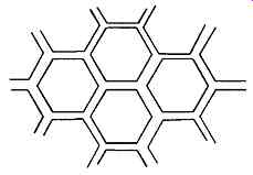
FIG55 Honeycomb construction of parallel connected MOSFET cells
For N-channel devices gm values in the range 0.5-1.5 S/ampere are usual, with P-channel devices falling mainly towards the lower end of this range. They will not, therefore, lend themselves to high gain stages, but they are very linear. Like junction FETs, they have an extremely fMIJVa curve, shown in FIG57, so that they can, within their permissible operating volt age range, make excellent constant current sources, and high dynamic impedance loads.
Two points which must be remembered in relation to power MOSFETs are that, because of their excellent high frequency characteristics, they can readily break into unwanted -- and possibly destructive -- oscillation as a result of the internal capacitances of the device, and the unavoidable inductance of the gate and source leads. This tendency to parasitic oscillation is best avoided by ensuring that the gate and source leads are as short as possible, and that they don’t run parallel to one another, and by including a 'gate stopper' resistor, of 50-330 ohms value, as shown in FIG58. The second point is that, as a function of their method of manufacture, as with Darlington type power transistors, all power MOSFETs have an internal diode, also shown in FIG58, which has identical reverse breakdown voltage and forward current carrying characteristics to the MOSFET itself.

FIG58 Gate stopper resistor connection
As with the small-signal versions of this device, the Vg/Ia characteristics are very linear, once within its conducting region, and this encourages the use of such devices as the output emitter followers (actually source followers) in the output stages of high quality audio amplifiers. Provided that their gate-channel breakdown voltage limitations are respected, and they are operated within the boundaries of the safe working area domain, shown in FIG59, MOSFETs, as a whole, can be used in most of the circuit layouts shown above for bipolar transistors, allowing for their some what different operating characteristics, and, as an example of the simultaneous use of bipolar transistors, junction FETs and MOSFETs, a 40-50 watt, very high quality, audio amplifier is illustrated in FIG60. In this circuit, internal loop negative feedback is employed (see Section 7) to stabilize the performance of the circuit, and to reduce the extent of residual waveform distortions to allow, for example, a total harmonic distortion (THD) of less than 0.01%, at full output power, over the frequency range 200Hz - 10 kHz.
MOSFET
Safe operating area for typical power
However, in order to avoid HF instability, some loop stabilization components such as Ca, the 'Zobel network', CyJRb, and the output inductor, Lc, must be included; particularly in order to avoid the possibility of malfunction when used with a reactive load, such as a loudspeaker unit.
An application for which both junction FETs and MOSFETs are well suited, but especially MOSFETs, is analogue signal switching, and this is covered in a later section.
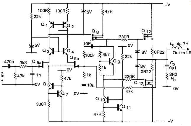
FIG60 High quality MOSFET output audio power amplifier.
Protection from gate breakdown Although power MOSFETs don’t suffer from the type of secondary breakdown which can damage power transistors due to the funneling of the emitter/collector current through small regions of the base-emitter junction, and the excessive localized heating which this will cause, they can fail catastrophically if the breakdown voltage of the gate insulating layer is exceeded.
Because power MOSFETs have very high gate channel capacitances, up to 3nF in some designs, they are much less susceptible to inadvertent damage due to induced electrostatic charges during handling, than the small signal devices, whose gate-channel capacitance may only be a few pF. On the other hand, it’s not practicable, in high power devices, to diffuse a pair of protective diodes, connected to the gate electrode as illustrated in FIG61, into the MOSFET chip, as is customarily done with small signal devices, since this can lead to thyristor-type '4 layer' (PNPN) type breakdown, which would be destructive in a high power circuit.
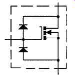
FIG61 Gate protection for small signal MOSFET
There is, however, no difficulty in using externally connected zener diodes, as shown in FIG60, to prevent some safe level of gate-channel voltage from being exceeded, and this is a sensible precaution. A somewhat less obvious reason for destructive gate channel breakdown can be seen from FIGs 53 and 54, in that there are regions of the transistor in which the gate metalizing is in proximity to that part of the transistor which is connected to the drain. In this case, where the gate-drain voltage exceeds the gate break down potential, the device will only survive so long as the voltage drop across the N-path between the channel and the drain is sufficiently greater than that across that part of the channel opposed to the gate electrode for the gate-drain voltage not to be exceeded, and the relative apportionment of these voltage drops will be drain current dependent. This means that under dynamic conditions, where both high drain currents and large gate-drain voltages can coexist, even briefly, gate insulation breakdown can occur, even though the limitation imposed by short-term thermal dissipation had not been exceeded, and this is a source of possible failure which must be considered.
Even so, the reliability of power MOSFETs, for high power use under difficult load conditions, is generally very much easier to ensure than with nominally equivalent bipolar junction power transistors.
Voltage reference sources:
In many linear circuit applications, such as, for example, the DC amplifier layout of FIG14b, or the current source of FIG16., a device giving some constant potential drop, or a local source of some reference voltage is needed. The simplest answer is to use a suitable zener or avalanche diode, but these will introduce a certain amount of wideband noise, which may be unacceptable for some circuit applications. In this case, it may be preferable to use a string of small signal diodes, connected in their 'forward', i.e. conducting, mode and to choose a sufficient number of these to build up the required voltage drop from the sum of the individual 0.57-0.6V diode voltage drops, since a junction diode operated in its forward mode is a relatively low noise device.
DC Amplifiers
Requirements for stability of output voltage level
Most of the circuit applications described above have been aimed at voltage amplification, or impedance conversion, functions in which the absolute DC value of the output voltage level was not important, provided that it stayed within some satisfactory working voltage range. However, the need arises from time to time to amplify a small DC voltage signal so that it can be used to give an instrument reading, or operate some mechanism requiring a higher power input. In these cases the absolute DC voltage level at the output will be important, and 'drift' in this value, for a constant input voltage signal, must be avoided.
As has been shown in FIGs 12a, 42 and 57, the collector or drain currents, for a fixed base or gate potential, of both bipolar junction transistors, and junction and MOSFET type field effect devices, are strongly temperature dependent, so that the output voltage any amplifier circuit using these components will be affected by changes in the ambient temperature of the devices, and also by any heating effects brought about by internal thermal dissipation.
FIGs 44, 49, 51 and 56 show that, for both junction FETs and MOSFETs, there is some value of gate voltage, depending on the device design, for which the temperature dependence of the drain current can be eliminated or minimized. This is a helpful circumstance, but, in general, the lessening or elimination of such voltage offset drifts due to thermal changes will be achieved by the use of the long-tailed pair arrangement of FIG15a, or the base-emitter offset potential cancelling layout of FIG62, or by using differential amplification techniques, as shown in FIG63, in which the comparative rather than the absolute value of the output voltage is used, for example, to operate a voltmeter. All of these approaches should be combined with means for keeping thermal dissipation effects, within the active devices, to the lowest possible level, by using the lowest usable working voltages and currents.
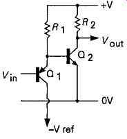
FIG62 Base-emitter offset voltage cancelling circuit
For very high degrees of long term DC stability, the amplifier unit may be enclosed in a temperature con trolled housing, or use 'chopper stabilization of the kind shown schematically in FIG64. In this, in FIG63 principle, the input DC signal voltage is converted into an AC voltage waveform by chopping it into a train of pulses whose peak amplitude is equivalent to the original input DC level. This pulse train can then be amplified by a conventional AC amplifier, whose AC gain is stabilized by the use of loop negative feedback (see Section 7). The amplified AC signal can then be converted back into a DC output voltage by means of some conventional rectifying' circuit. Commercially available DC amplifiers, particularly those in 'hybrid' form (i.e. encapsulated blocks containing surface mounted discrete components) may contain all these functions within a single package.
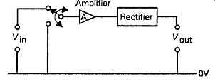
FIG64 Chopper stabilized DC amplifier; Amplifier; Rectifier
These chopper stabilized hybrid amplifiers tend, however, to be costly, and the performance they offer is being approached by more conventional, and much less expensive, operational amplifier IC packages, and it’s suggested that the use of these ICs should be considered when DC amplification is required.
These linear IC DC amplifiers either employ quite normal circuitry, with the components and layout optimized to ensure very low DC drift in the input and output offset voltages, such as the ??G ??07' and 'NS' 'LM12T ICs, or so-called chopper systems, such as the National Semiconductors 'LMC668', in which a normal amplifier stage is arranged so that its zero setting is continuously trimmed by a further amplifier within the IC package, as shown schematically in FIG65. This arrangement employs two nominally identical amplifier packages, A1 and A2, which have external Offset null' correction points, p and q. These amplifiers are connected to internal CMOS switches, S1 and S2a/S2b, operated by an external 'clock'. At the beginning of the switch cycle, the two inputs of the 'nulling amplifier', A2 are shorted together, and its output is connected to the two nulling points, through S2a and S2b. In the case of A2, this generates a DC negative feedback loop which operates to zero the DC output voltage, and this correction, being applied to Ax as well, has the effect of generating the necessarily offset which would have been required to cancel any output errors in A19 had its inputs been short-circuited as well. In the interval between the switching cycles, the required zero adjust voltages are stored in two (external) low leakage capacitors, C1 and C2 Quoted long-term output voltage drift levels for the LMC668 are of the order of 100nV/month.
Thermal drifts in the other circuit components, of which the principal ones likely to affect the results in amplifier and other signal handling circuitry are the resistors, have now been reduced to very low levels by the choice of optimum constructional materials.
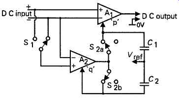
FIG65 Integrated circuit chopper stabilized operational amplifier
The final effect which can cause DC drift, in amplifiers and other circuitry, is the change of component characteristics due to ageing, and to a lesser extent, due to thermal cycling and mechanical vibration. Once the initial bum in time has elapsed, ageing effects in semiconductors, when operated well within their maximum permissible voltage, current and working temperature ratings, arc relatively small by comparison with those found in thermionic valves, where the mechanical changes due to internal outgassing and gradual loss of cathode emission are continuous throughout the lifetime of the device.
