AMAZON multi-meters discounts AMAZON oscilloscope discounts
[cont. from part 1]
Operational amplifier systems
Operational amplifiers, devices which are now readily available as integrated circuit functional blocks, are basically amplifier units in which the internal circuit design and 'HF compensation' arrangements are such that they will operate stably with 100% NFB -- a condition in which the output pin is connected directly to the inverting input pin, as shown in FIG23. -- an arrangement which, incidentally, provides a wide bandwidth, unity gain, 'buffer' block, having a high input impedance and a low output impedance.
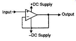
FIG23 Operational amplifier connected as unity gain buffer stage.
Commercial opamp ICs are normally operated from a pair of +ve and-ve supply lines, typically over the range +/-3V to +/-18V, depending somewhat on device type. (+/-15V is the most common maximum supply voltage value for normal commercial components, although there are some devices specially de signed to operate from much higher or lower supply line potentials.) It’s also normally practicable, by the use of a suitable circuit layout, to operate these devices between a single supply line and the 0V rail, and some opamp types arc designed specifically for this type of application, with the 0V level being part of their input signal range.
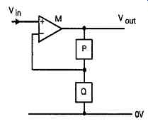
FIG24 Connection of opamp as series feedback system
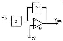
FIG25 Connection of opamp in shunt feedback system.
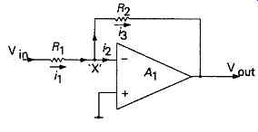
FIG26 Basic 'shunt feedback' layout.
Negative feedback can be applied either as series feedback -- the method considered above, in which the feedback signal is applied in series with the input signal -- or as shunt feedback, in which the input signal and the feedback signal are simultaneously applied to the inverting input of the opamp., as shown respectively in FIGs 24 and 25. Although both of these methods of feedback connection have a virtually identical effect upon the output impedance and band width of the system, they are not identical in respect of gain and internal distortion, and have very different effects upon the input impedance of the circuit.
In the case of the series feedback system shown in FIG24, in which the amplifier, M, has an open loop gain of A.
…where ß is the proportion of the output signal fed back by the feedback network [Q/(P + Q)], V\ is the actual voltage appearing across the input of the amplifier block, and Ra is the input resistance of the amplifying block. The input resistance of the circuit…
In the case of the shunt feedback layout shown in FIG26, if we define the circuit input current through R1 as n, the amplifier input current as i2, and the current through the feedback resistor, R2, as i3, then:
The impedance at the input point, X, of an amplifier using shunt feedback can be determined, approximately, by the following argument:
Let us postulate an ideal amplifier, in which neither of the inputs will draw current, so that i\ = 13. How ever, because M is an inverting amplifier, the voltage across R2 will be …
Since this can be very low indeed if A is high enough -- much lower in practice than the input impedance of any likely amplifier circuit--neglecting the amplifier input current, j'2, does not significantly affect the result.
The very low impedance at this point gives rise to the common term applied to the input of an inverting amplifier with feedback as a 'virtual earth', and allows the circuit arrangement shown in FIG27 to be used as a summing amplifier, or signal mixer, with very little interaction between the separate inputs, a, b and c, etc.
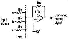
FIG27 Application of shunt feedback system, as input mixer stage. Input signals;
Combined output signal 4-0V
Another important difference in the way of operation of the series and shunt feedback layouts shown in FIGs 24 and 25, is that the gain of the shunt feedback layout can be made to fall to zero, if that part of the feedback network, P, is reduced to zero, whereas the gain for any series feedback system can only be reduced to unity if the limb P is made to have zero impedance. This difference in characteristics can be important when the impedances of limbs P and Q are made frequency dependent, as in frequency response shaping applications.
In both the shunt and series feedback circuits, the application of negative feedback will lower the output impedance of the amplifying block, at the point from which the feedback path is taken. The magnitude of this effect can be calculated by considering the case of an amplifier, which has a gain A, and an effective output resistance, without feedback, R0, which has its non-inverting input grounded, and which has a feed back signal returned to its inverting input through the attenuator network B, as shown in FIG28. If a voltage V is applied to its output, this will produce a feedback signal at the inverting input of the amplifier having a magnitude BV. Since the input is an inverting one, this will give rise to an output from the amplifier, Vout=-ABV. The voltage across R0 (Vo)> will be given by:
…so the output impedance, with feedback, R'0, which is V/I0, will be:
This effect is the same for both series and shunt feedback systems.
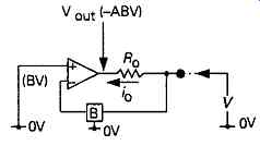
FIG28
The principal use of the series FB system, shown in FIG24, is to isolate the input signal from the feedback network, and allow the input impedance to be determined independently of other considerations, as shown in the gramophone input RIAA equalization stage of FIG29, where the required input load is commonly 47k-Ohm.
As mentioned above, a common application of such feedback systems is in the field of frequency response shaping circuitry, in which the networks P and Q, in FIGs 24 and 25, may contain combinations of capacitive, inductive and resistive elements, so that the LM833 Equalized signal output gramophone< pick-up.
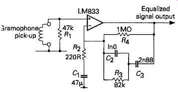
FIG29 Gramophone pick-up input amplifying stage with R.I.A.A. type frequency
response equalization impedance of the feedback limbs will depend on frequency,
which will alter the circuit gain, as a function of frequency.
In all cases, where negative feedback is applied around an opamp, care should be taken to make sure that any feedback network connected between the output and the input of the operational amplifier does not cause it to operate beyond the maker's design limits for closed-loop stability, a consideration which is explored later on in this section. The design of these ICs will normally be chosen so that there is an adequate safety margin for all normal uses, but the possibility that the external feedback networks may influence the opamp performance is a point which should be borne in mind.
Effects of negative feedback on distortion
It’s normally assumed that steady-state nonlinearities in any amplifying circuit will be reduced in direct proportion to the extent by which the gain of the system is reduced by negative feedback. It has been noted earlier that this assumption will only be strictly correct if the feedback is truly negative, and if the gain of the system is the same for all of the frequencies associated with the harmonic components introduced by the distortion of the signal as it’s for the fundamental frequency of the waveform. However, there is also the fact that if the amplifier introduces, say, 2nd and 3rd order harmonics, these components will be present in the feedback signal, and will, in turn, be distorted in their passage through the amplifier. So, while the anti-phase 2nd and 3rd harmonic feedback components will tend to cancel those introduced by the amplifier --and thereby reduce the magnitude of these unwanted signals present in the output -- the nonlinearities, and the intermodulation effects of the amplifier, acting on these reintroduced signals will generate higher order, and probably less desirable harmonic components.
A graphical illustration of this phenomenon, due to P. J. Baxandall (Wireless World, December 1978), showing the way in which the magnitudes of the harmonic components alter as the amount of negative feedback is increased, based on measurements made on a simple FET amplifier stage, is shown in FIG30.
Amount of negative feedback
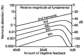
FIG30 Effect of increasing amount of NFB on distribution of harmonics in
simple FET amplifier stage.
A further point related to the distortion of a feedback amplifier stage is that less distortion, other things being equal, will always be given by a shunt feedback circuit, in comparison with a series feedback layout.
The reason for this is shown, using the example of a junction transistor input stage, in the circuit diagrams of FIGs 31 and 32.
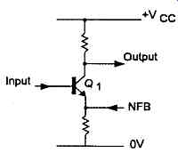
FIG31
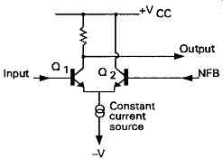
FIG32
In the first of these, where the NFB is applied to the emitter circuit of the input transistor, while the input signal is applied to its base, the assumption is made that the base-emitter potential of the input transistor will remain constant, throughout the excursions of the input signal. Unfortunately, this is not a valid assumption, since the base-emitter potential will vary as the emitter current changes during the transmission of a signal. This will add a voltage component (related to the input transistor signal) to the feedback voltage, and impair its effectiveness in reducing the amplifier distortions. This leads to a worsening of the distortion as the magnitude of the input signal is increased.
In the long-tailed pair input circuit of FIG32, most commonly used in operational amplifiers and other good quality amplifier systems, the problem of collector current modulation of the input base-emitter voltage in Q1 is somewhat lessened because of the compensating effect of the balancing transistor Q2.
The way this happens is that if a positive-going signal voltage is applied to Q1, which will increase its collector current and its base-emitter offset voltage, then this will cause a reduction in the collector current of Q2, since both transistors are fed from a constant current source. This will then reduce the base-emitter offset voltage of Q2, which will consequently increase the size of the NFB voltage applied to Q1 emitter by an amount which is closely equivalent to the increase in the base-emitter offset voltage of Q1. The result of this is that the sum of the base-emitter potentials of Q1 and Q2 tends to remain constant, so that there is more effective coupling of the feedback voltage into the feedback loop. Nevertheless, even in well designed amplifiers, the input signal voltage will have an effect on amplifier distortion, especially on those circuits which have a 'single-ended' input, such as that in FIG31.
This effect is well illustrated in the manufacturer's application note for the 'single-ended' Harris A-5033 buffer amplifier IC, for which the internal circuit and the relationship between input signal voltage and harmonic distortion is shown in FIGs 33 and 34.
However, even in circuits with an input long-tailed pair arrangement, of the type shown in FIG32, there is a residual difference in closed-loop distortion, as shown in the data sheet for the Texas Instruments LT1028, and shown in FIG35, for various values of closed-loop gain (Av). The extent to which such an amplifier is immune to the effect of a simultaneous application of input and feedback signals is known as the 'common-mode rejection ratio', and, for a competently designed opamp., will normally be of the order of 100dB or more, although, like many other quoted parameters, it’s likely to be quoted for the most favorable circumstances, and like other qualities it will get worse with increasing input signal frequency.
In a shunt feedback arrangement, there is no common mode signal, so the rejection ratio will always be infinite!
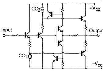
FIG33 Slightly simplified circuit layout of Harris A-5033 buffer amplification
Appendix
Operational amplifier parameters
There are many other aspects of opamp performance characteristics which one would normally expect to be specified in the manufacturers' data sheets and these will relate to both the steady-state and the dynamic operating conditions of the device.
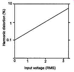
FIG34 Input signal voltage/distortion characteristics of A-5033
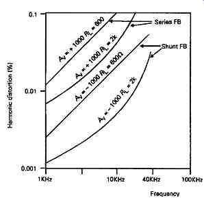
FIG35 Comparison of distortion characteristics of series and shunt NFB
in high quality opamp.
Slew rate
Among the latter, an important characteristic in relation to the HF performance of the amplifier is the slew rate -- the maximum rate at which the output voltage can change when it’s presented with an instantaneous change in its input voltage. This has a rigid limit- for reasons explained above in discussing the HF stabilization of the amplifier circuit shown in FIG20 -- because the design choice for this purpose is almost invariably the use of a 'dominant lag' capacitor, in the circuit position C1 in the analysis of this circuit. This parameter will be defined in terms of a slope, in volts/microsecond, and will usually be somewhat different for positive- and negative-going waveform edges. If loss of signal during this slewing process cannot be tolerated, then either the size of the input signal must be restricted so that the required output voltage change does not exceed the slewing capability of the amplifier, or the high frequency components of the input signal must be curtailed by a simple input RC network, of the kind shown in FIG11.
Gain bandwidth product (GBP)
This characteristic, like many other specifications offered by manufacturers, is misleading, in that it appears, at first sight, to indicate the usable bandwidth of the device. However, this is, in reality, very much less than the quoted value, since the gain bandwidth product defines the point at which the opamp gain falls to unity, and an amplifier with an open-loop gain of unity is unlikely to be of much use.
So, if the minimum open-loop gain which will be of use is, say, 10, then the maximum HF bandwidth will be the GBP value divided by ten, and so on.
Power supply rejection ratio (PSRR)
It will be obvious that the performance of any electronic circuit could be impaired if there is unwanted and unexpected intrusions of noise, hum or ripple, from the supply lines into the signal channel, and most data sheets will quote values for the ability of the circuit to reject such breakthrough.
However, although a value of, say, HO dB (300,000:1) may be quoted, which would appear to be excellent, it will probably be worse for the negative supply line than for the positive one, and, in both cases, will deteriorate with increasing frequency, so that it may only be 20dB (10:1) for a 300kHz supply line signal, as is the case for the 'LM312' IC. The values quoted should always be for open-loop operation, since the application of overall NFB will improve this figure, in any case, except at higher frequencies where the internal phase shift of the device is significant.
Output voltage swing
This is influenced both by the supply line voltage and also by signal frequency, since it will decrease beyond some point at which slew rate limiting begins to occur.
The makers graphs of this parameter, as a function of frequency, are a much better guide to the HF performance of the device than either the GBP or the quoted slew-rate figure.
Other characteristics---Many other operating characteristics will also usually be quoted, which may allow the optimum choice of a particular type of opamp for a particular application.
With high impedance circuitry, a low value of input bias current -- the input base currents required by the input transistors -- is desirable, though, for very high impedance circuitry, where very low amplifier noise is not also an essential quality, a JFET- or MOSFET-input opamp may be the preferred choice.
In amplifiers designed for low noise operation, one would also expect to find details of the equivalent input noise voltage, in nano-volts/__/Hz. Other details, such as output DC offset voltage, supply current, voltage gain, and the permissible or practicable input or output voltage swing, will also be given, together with information on the gain and phase margins of the device, to provide some guidance on the likely stability of the amplifier when negative feedback is applied. This is likely to be affected by output load characteristics, especially if these are inductive or capacitative.
It’s becoming increasingly common for opamp ICs to employ internal HF compensation so that they can be used (but usually only on a resistive output load) with 100% NFB (as a unity gain buffer) without danger of HF instability, even though this will lead to a rather poorer HF response than would have been possible if the device had only been compensated for the closed-loop gain level appropriate to its intended use. For this reason, there are still a few externally compensated opamps, available, for which the manufacturers will supply details of the necessary components which will be required to be connected to the device to ensure stability at a given closed-loop gain level. The data sheets may also, if one looks for it, give information on permissible load characteristics, where these affect closed-loop NFB stability.