AMAZON multi-meters discounts AMAZON oscilloscope discounts
(cont. from part 1)
So, with regard to the specification of filters, in addition to whether an HP or an LP type is required, and the desired turn-over frequency and attenuation rate, it’s also necessary, in the case of the Chebyshev or Cauer forms, to stipulate the extent of 'ripple' -- both within and beyond the pass-band -- which is accept able. In the case of multiple pole LCR filters used in RF circuitry, filter design has become a highly specialized field, which is largely outside the scope of this guide.
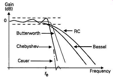
FIG33 General form of filter characteristics (illustrated for low-pass
systems): Gain (dB); Butterworth; Chebyshev; Bessel; Cauer; Frequency
Although the simple circuit shown in FIG31a does work, and would come within the broad category of active filters, it’s a rather crude approach to the design of such systems, of which a number of quite elegant circuits have been evolved by circuit engineers. As an example of such a design, an immediate improvement can be made to the performance of the circuit of FIG31a, by adding a further capacitor, C3, between the 0V line and the junction of Rx and R2, as shown in FIG34a. This substitutes an external phase shifting capacitor, C3, in the feedback path, in place of the incidental phase lag due to the amplifying block, and converts the circuit into a simple 'second order' filter system (i.e. one in which the characteristics are determined by two phase shifting elements, such as, in this case, the two RC networks), which has a Butterworth characteristic and a -12 dB/octave attenuation rate beyond the turn-over frequency, as shown in the graph of FIG34c. The layout shown in FIG34b is a simple modification of this circuit, which also gives excellent results, in which C1 is introduced in the NFB limb. Its value will require to be reduced, in relation to that used in FIG34a, by the amount A'+1, where A' is the gain of the amplifier after feedback has been applied. Both of these layouts are useful in that the filter will also provide gain, determined by the ratio R3:R^ A common application for a high-pass filter is to eliminate turntable 'rumble' in Hi-Fi audio equipment. This facility was often provided in earlier equipment designs, at a time when neither the turn-tables in domestic use, nor the record manufacturers' cutting lathes were as well engineered as they are now, and LF noise intrusion due to inadequate turntable bearings could be audibly objectionable. Such a rumble filter will usually require to have a ruler flat frequency response down to, say, 32Hz, and as rapid a rate of attenuation as is practicable (usually at least -20dB/octave), below this frequency, in order to exclude rumble components in the 2-10Hz frequency range without significantly reducing the magnitude of the wanted VLF components of the signal.
A typical circuit layout for this purpose is shown in FIG35. This incorporates a high-pass filter net work within the negative feedback path of a gain stage.
The frequency response generated by this circuit is shown in FIG36. A particular advantage of this kind of circuit is that the gramophone record replay frequency response correction network (the RIAA network), can also be connected between the output and inverting inputs of the amplifier, in parallel with the rumble filter components, without impairing the operation of this filter. This circuit is actually a filter of the general type classed as a bridged T design, which are usually con figured as 'third-order' (-18 dB/octave) designs, with some external passive element, in this case the input capacitor/resistor network, C1R1, used to remove the characteristic hump in the response curve at the turnover frequency.
The somewhat simpler circuit layout of the bridged T, when used as a low-pass filter as shown in FIG37a, can be used to illustrate this point. With the component values shown it will give the response curve shown in FIG38, with a prominent hump at 1kHz. If an additional RC low-pass network, R4C3, is added to the circuit, as shown in FIG37b, the hump can be flattened out to give a Chebyshev type of response, with a +/-3dB ripple, as shown in FIG39.
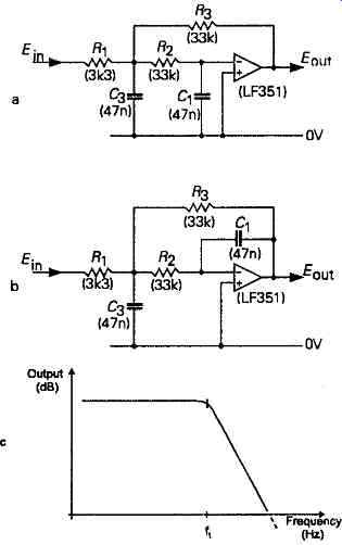
FIG34 Improved active low-pass filter circuits (component values quoted
are for ft = 1 kHz)
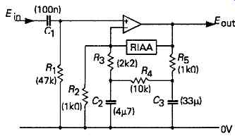
FIG35 Hi-Fi rumble filter circuit (ft = 32Hz)
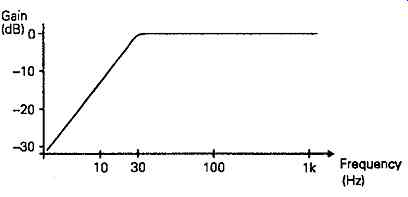
FIG36 Frequency response of circuit of FIG35
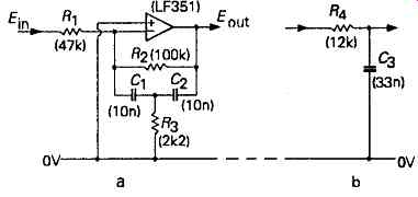
FIG37 Bridged-T filter (ft = 1Hz)
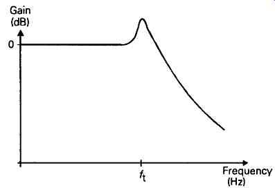
FIG38 Frequency response of FIG37a
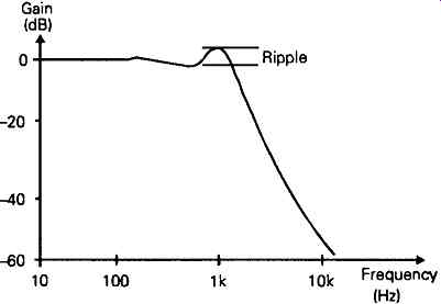
FIG39 Frequency response of circuit of FIG37 with addition of R^Cj network
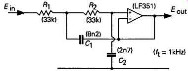
FIG40 Low-pass Sallen and Key filter circuit
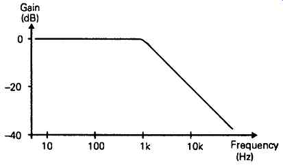
FIG41 Frequency response of circuit of FIG40
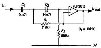
FIG42 High-pass Sallen and Key filter circuit
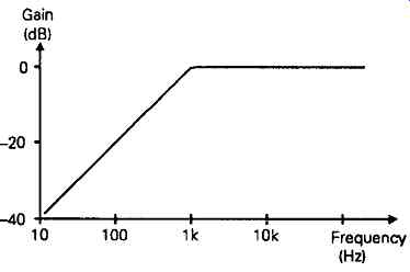
FIG43 Frequency response of circuit of FIG42
Two important categories of filter are the 'Sallen and Key' (Sallen, R. P., and Key, E. L. J RE Trans. Circuit Theory. March 1955, pp. 40-42), and the 'bootstrap' (JLH, Electronic Engineering, July 1976) filter types, which are built around unity gain impedance converter blocks -- though, with some adjustments to the circuit, they can also be employed with stages giving gain. The big advantage of these layouts is the ease with which the circuits can be transposed to give either LP or HP versions. Considering the Sallen and Key design first, this uses the layout shown, for a low-pass filter, in FIG40. This gives a second-order response (-12dB/octave), with a Butter worth type of characteristic, as shown in FIG41.
A high-pass version of the same kind of circuit, in which the position of the resistors and capacitors has been interchanged, is shown in FIG42, with the frequency response illustrated in FIG43.
A circuit curiosity is that this kind of filter can be further elaborated as shown in FIG44, to employ four pairs of RC networks. Sadly, this layout does not give the expected -24dB/octave attenuation rate, but only some -20dB/octave, as shown in FIG45. In the application in which it was shown (Philips Components and Applications, August 1980, pp. 215-218), it was used simply as a means of generating a time delay in the signal path.
As noted above, Sallen and Key filters of this design will usually be con figured to have a Butterworth characteristic. By contrast, the bootstrap designs are usually arranged as third-order Chebyshev response systems, with atypical pass-band ripple of +/-1dB and an initial attenuation rate of -20dB/octave. A suitable circuit design for a low-pass filter of this type is shown in FIG46, with the frequency response as shown in FIG47.
The equivalent high-pass bootstrap design is as shown in FIG48, for which the frequency response is shown in FIG49. The method by which the bootstrap filter operates can be visualized by considering the effect of R2C2, or C2R2, *n the feedback path. At frequencies within the pass-band of the filter, the impedance of the feedback limb is low in relation to that of the lower input limb, which has the effect, by bootstrap action, of making the impedance of the upper half of the input limb (R1 or C1), appear to be high, so that there is little input signal attenuation.
However, as the turn-over frequency is approached, the change in relative impedances of the feedback and lower input limbs causes the effectiveness of the boot strap action to diminish, which causes the input circuit attenuation to increase, and so on.
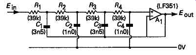
FIG44 Four element Sallen and Key filter
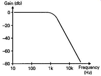
FIG45 Frequency response of circuit of FIG44
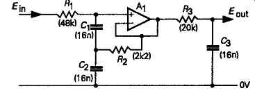
FIG46 Low-pass bootstrap filter (f = 1kHz)
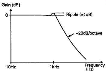
FIG47 Frequency response of circuit of FIG46
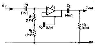
FIG48 High-pass bootstrap filter (f = 1kHz)
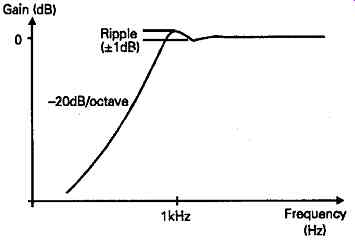
FIG49 Frequency response of circuit of FIG48
The turn-over frequencies of both the Sallen and Key and Bootstrap designs are given by the equation … though due allowance should be made for possible inaccuracies in component values.
The specific component values for the bootstrap filter can be calculated, in the case of a third-order low-pass filter, from the relationships:
In the case of a third-order high-pass filter, the values are given by …
In practice, the calculations can be simplified by making the ratio y equal to unity, which is satisfactory for general use. For a typical Chebyshev response, with a ripple between +/-1dB and +/-3dB, Q values between 1.8 and 2.2 should be chosen.
Although I have shown most of the preceding filter designs with component values chosen to give a 1kHz turn-over point, they can be con figured for different frequency values by simple proportional adjustments to the values of the resistors and capacitors.
The filter designs shown, so far, have allowed the generation of cut-off slopes up to some-20dB/octave.
In applications where a steeper attenuation rate is needed the simplest solution is merely to connect two or more filter blocks, tuned to the same frequency, in series. Care should be taken, depending on the type of filter, to ensure that the pass-band ripple is not made unacceptably high by this process -- perhaps by combining circuits of Butterworth and Chebyshev characteristics -- and that the output and input impedances of the succeeding stages are compatible.
A further possibility which can be of interest in sharpening up the cut-off slope of a simple filter system is by combining it with a notch filter -- especially if the whole arrangement is included within the negative feedback loop to flatten out the frequency response of the system within the required pass-band.
The cut-out response curve given by this type of arrangement will generally be of the Cauer type, with a pronounced ripple in the transmission characteristic beyond the cut-off point. This type of filter system is examined below in the section covering notch filters.
Variable slope filters
The cut-off slopes given by the simple CR filter types of FIGs 1c and 1d can be lessened by reducing the value of the resistor, Rc, across the capacitor or inductor, and this approach has been used in some commercial Hi-Fi circuitry where the network is used as a treble hiss filter.
A rather more elegant option is as shown in the case of the low-pass and high-pass bootstrap filters shown in FIGs 50 and 51, where if a variable resistor, RVV is inserted in the return paths of C3 or R3, as shown, the slope and characteristics of the circuits can be adjusted to provide frequency response curves which approximate to either Chebyshev, Butterworth or Bessel, as needed. This can be advantageous in audio circuitry since all filters, having a cut-off slope beyond some -6dB/octave, will introduce some degree of tonal coloration, particularly noticeable with low-pass filter systems in the mid- to treble band, where the peak in the voltage response as a function of time -- illustrated in FIG52 for a square-wave input signal -- characteristic of all steep filter cut-off rates, will tend to concentrate wide-band signal energy (e.g. that due to broad-band signal or noise components) in the region of the cut-off frequency, thereby giving it a degree of tonality.
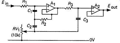
FIG50 Variable cut-off slope LP filter
Notch filters
Two types of CR network are commonly used to generate a null output at some chosen frequency: the parallel-T, also known as the twin-T, and shown in FIG19, and the Wien network, often called the Wien Bridge, shown in FIG53.
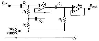
Fig. 51 Variable cut-off slope HP filter
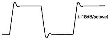
FIG. 52 Influence of filter slope on square wave waveform
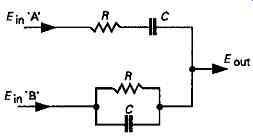
FIG. 53 Wien network
Considering the Wien circuit first, the impedance of the upper limb will be nearly infinite at some very low frequency, but will decrease with increasing frequency as the impedance of C decreases, until, at some very high frequency, the impedance of this limb will approach the value of R. However, the lower limb has an impedance at VLF equal to that of R, and it will continuously decrease with increasing frequency as the impedance of C falls, asymptoting to zero. At some intermediate frequency, at which the impedance of C is equal to R, the impedance of the upper limb will be twice that of the lower, but the phase shift in each limb will be the same. This means that if this network is fed with signal inputs at A and B, and if these two inputs are in anti-phase, and it’s arranged that the input at A is exactly twice the magnitude of that at B, then the two signal currents at X will exactly cancel at that frequency at which the impedance of C is equal to R, or, f0=1/(2 pi CR).
If an inverting amplifier having a gain of two is interposed, as shown in FIG54, to provide the required antiphase upper limb input, the attenuation characteristics of the circuit, as a function of frequency, is as shown in FIG55. With the component values indicated, f0 is approximately 1kHz (actually 994.7Hz).
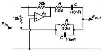
FIG54 Null network using Wien bridge
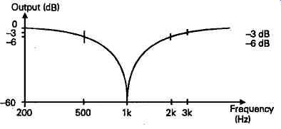
FIG55 Performance of circuit of FIG54 In the case of the parallel-T circuit,
its method of operation can best be explained by considering the attenuation
and phase shift given by each of the two limbs. In the RCR limb shown in
FIG56, the phase shift of the output voltage in relation to that of the input
is -63.44° at the frequency at which the phase shift of the CRC limb, shown
in FIG57, is +63.44°. Since both networks will give the same attenuation
at this frequency (994.7Hz for the values suggested), their combined outputs
will cancel -- which means that the circuit will give zero output at this
frequency.
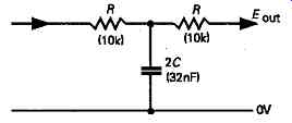
FIG56
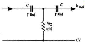
FIG57
The use of a gain block to sharpen up the notch given by a parallel-T filter was mentioned earlier, and the circuit layout was shown schematically in FIG19.
The effect on the notch characteristics of the network of a voltage feedback signal derived from the output of the gain block, using the circuit layout of FIG20, can be seen from FIG19, in which the solid line shows the attenuation characteristics of the parallel-T network on its own -- when RVX is set to give zero feedback -- and the dashed line shows the effect with RV1 set to give maximum feedback. Intermediate settings of RV1 will give intermediate degrees of notch sharpness.
However, the same type of approach can also be used to sharpen up the characteristics of other circuits of this type, such as the Wien network shown in FIG58, as Ra,Ca/Rb,Cb -- where NFB applied around the loop can be used to modify the response curve from that shown in the solid line of FIG59 to that shown in the dashed line. This kind of layout, because the actual notch frequency can be tuned by adjustment of Ca and Cb, which may, conveniently, be a pair of air-spaced dual gang capacitors, provides a useful basis for a 'total harmonic distortion' type of distortion meter, in which the residues of a notionally pure sinewave signal, after the fundamental frequency has been notched out, are presumed to be the harmonic distortion components together with any circuit noise and hum.
In the circuit of FIG58, the input buffer amplifier, A1, is used to provide a high input impedance, a low drive impedance for the Wien network R5/C1 and R6/C2, and also to provide a means by which NFB can be used to sharpen up the notch -- by way of the feedback path from A3 output, via Rn, to the resistor in the inverting input circuit of A,. A2 provides the required phase inversion and the two times increase in the signal voltage applied to R6/C1, with respect to that applied to R6/C2, needed to cause the network to provide zero transmission at the frequency determined by fo=1/(2 pi CR)
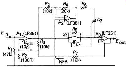
FIG58 Total harmonic distortion meter circuit based on Wien bridge network
using NFB to sharpen up notch response of circuit.
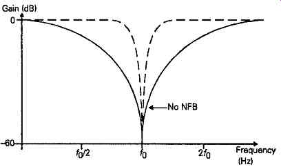
FIG59 Effect of NFB
...where the values of R and C are R^R^ and C1=C2. The need to sharpen up the notch arises from the need to ensure that the null network will pass the second and higher harmonics (2kHz, 3kHz, 4kHz etc.) at the same magnitude as the un-notched 1kHz fundamental, of which the value is determined by closing the switch, s1.
Clearly the simple circuit of FIG54; which gives the solid line response curve shown in FIG59; would not satisfy this requirement. On the other hand, too light a notch would be awkward in use, because of the great delicacy which would be needed to tune the circuit precisely to the null frequency. In the circuit example shown the amount of NFB is determined by the values of R3 and R7 in relation to R2.
Examples of published total harmonic distortion meter circuits are given in Section 17.
A notch filter can often be added to an existing active low-pass or high-pass filter circuit, and if the notch frequency is placed appropriately in frequency, and NFB is applied over the whole loop, the superimposition of the two curves can give a very high initial cut-off rate. An example of a circuit in which a parallel T notch filter is added to a Sallen and Key low-pass filter, is shown in FIG60, for which the overall frequency response is shown -- once again normalized to 1kHz -- in FIG61.
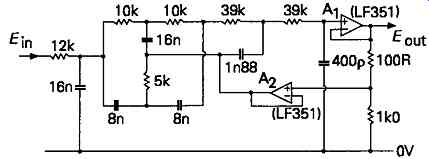
FIG60 Combination of Sallen and Key and parallel-T notch filter.
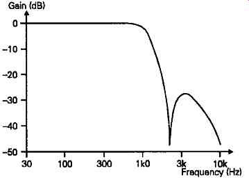
FIG61 Frequency response of circuit of FIG60
A similar layout to provide a steep cut-off high-pass filter is shown in FIG62, for which the frequency response is shown in FIG63.
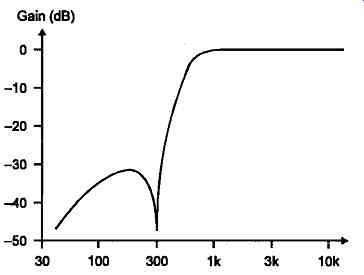
FIG62 High-pass filter using combination of Sallen and Key and parallel-T
filter
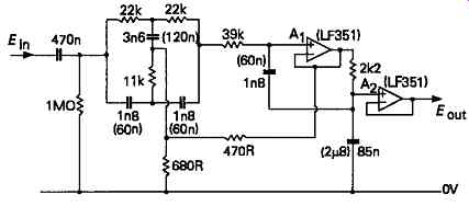
FIG63 Frequency response of circuit of FIG62.
The same kind of combination can be used with a bootstrap filter to give very high initial attenuation rates -- approaching -40dB/octave -- and with a skirt response which does not rise above -40dB at frequencies beyond the notch. Two circuit examples are shown, with component values chosen for/t values of 1kHz, in FIGs 64 and 65. The transmission graphs shown in FIGs 66 and 67, show the performance of the low-pass and high-pass designs respectively. The layout of FIG65 would make a splendid Hi-Fi rumble filter using the amended capacitor values shown in brackets, as appropriate for a 30Hz turn-over frequency, with an output below -40dB for signals of 14Hz and below.
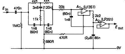
FIG64 Bootstrap and notch filter combination high-pass. Values in brackets
for ft = 30 Hz
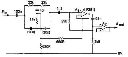
FIG65 Bootstrap and notch filter combination (f = 1 kHz)
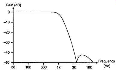
FIG66
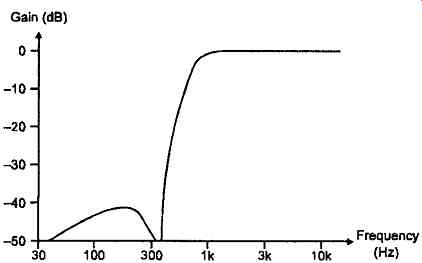
FIG67
Tuned response filters
The use of a parallel-T notch filter in the negative feedback path of an amplifier has been shown earlier, in FIG23, as a means of generating an increase in gain at some specific operating frequency. The same effect can be achieved by the use of a Wien network if it’s connected around a gain block in the same manner as in a Wien bridge oscillator, but with the amount of NFB adjusted so that the circuit just fails to oscillate. A suitable circuit arrangement is shown in FIG68, in which C1R1/C2R2 are the frequency determining components and RVX is used to set the circuit to just below the onset of continuous oscillation. The input signal can be injected into the inverting input of the opamp type gain block, using the virtual earth characteristics of this point to isolate the input signal from the feedback voltage.
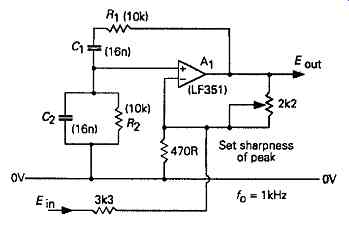
FIG68 Tuned response filter based on Wien bridge.
While this layout can give a very sharply tuned response, it suffers from the drawback that the actual circuit gain is critically dependent on the setting of RVV. A more predictable performance is given by the use of a pair of under-damped second-order active filters in cascade, as shown in FIG69, as a practical implementation of this arrangement. If the Q of each of these is set to give a response peak of, say, +6db, and the component values are chosen so that both filters operate at the same frequency, the outcome will be a circuit with a gain of + 12dB, at/0, and steep attenuation skirts on either side of this frequency.

FIG69 Tuned response filter based on cascaded bootstrap filters
Bandpass circuitry
The circuit shown in FIG26 is often advocated as a bandpass layout. However, in practice, the very low (6dB/octave) skirt slopes mean that it’s seldom of much practical use. A much better approach would seem to be to arrange a high-pass and a low-pass pair of suitable active filters in series, with op amp buffering in between them if necessary, to isolate their functions, as shown schematically in FIG70.
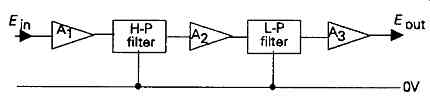
FIG70
Effect of filter slope on waveform shape
One of the characteristics of any filter which modifies the frequency response of a system is that it will cause a change in the shape of a step function, or square wave input waveform, and if the slope of a HP or LP filter is greater than -0dB/octave, this effect will be particularly marked. This is an effect which is particularly noticeable in the case of low-pass filters, where the result will be a pronounced ringing on the leading and trailing edges of the waveform, as illustrated in FIG52. This waveform distortion results from a combi nation of effects -- of which the alteration in the relative phase of the individual signal components which add together to make the square waveform; the removal of the higher frequency components; and the exaggeration of those frequency components lying close to the turn-over point due to any peaks in the transmission at this frequency, are the most important.
With a wide bandwidth input signal, for example white noise, the effect of a steep filter attenuation rate can be to modify the energy distribution of the input signal, and cause an increase in relative signal energy at or near the turn-over frequency. An additional point to remember is that alterations in the frequency response of any system will cause an associated change in the relative phase of the components of that signal within one decade of the turn-over frequency, and the steeper the filler slope, the greater this effect will be.