AMAZON multi-meters discounts AMAZON oscilloscope discounts
..
The ESR Zero
We ignored the ESR of the output capacitor in Fig. 14, and also in the list of transfer functions provided earlier. For example, earlier we had provided the following control-to-output transfer function for a buck ...where ?0 = 1/v(LC). The ESR zero adds a term to the numerator. A full analysis shows that the control-to-output transfer function now becomes ...
... where ?esr = 1/((ESR) × C) is the frequency (in radians per second) at which the ESR zero is located. Judging by the sign in front of the s-term in the numerator, this is a "well-behaved" (left-half-plane) zero. But it does increase the gain by +1 after the ESR zero location. So if the plant gain was falling at a slope of -2 (past its double pole, not cancelled), as soon as it encounters the ESR zero, its slope will change to -2 + 1 =-1.
If we were using only an op-amp integrator (no LC-pole cancellation), the open-loop gain will then fall with a slope of -2 instead of -3. But that is not enough. However, if we introduce just one zero (besides the pole-at-zero and the ESR zero), we can get the -1 intersection at crossover, as we are seeking.
However we should remember that ESR is a parasitic and is hard to control and define well.
In fact, vendors of capacitors rarely provide "min/max" limits for this parameter (usually assuming rather that the MAX of the ESR is the only concern to us). In addition, trace lengths will also contribute to the effective ESR, thereby changing the location of the ESR zero significantly from what we may have been expecting. In addition, the ESR zero is also likely to keep changing with respect to temperature, and also over time (especially for aluminum electrolytics). So the preferred strategy is to estimate rather crudely where the ESR zero is, and try to cancel its effect altogether - by means of a pole provided by the compensation network - at around the same location as the ESR zero.
In general, for making the control loop less sensitive to high-frequency switching noise, designers often put another pole roughly at about 10 times the crossover frequency (sometimes at half the switching frequency). So now the gain will cross the 0 dB axis with a slope of -1, but at higher frequencies it will drop off more rapidly, with a -2 slope. But why did we pick 10 times the crossover frequency? Because we know that the phase introduced by this high-frequency pole will actually start making itself felt at one-tenth the frequency of the pole, and we didn't want to adversely impact the phase angle in the vicinity of the crossover frequency (i.e. the phase margin). Later on we will realize that we can actually move this high-frequency pole much closer to the crossover frequency. In fact that is often desirable, because it "improves" the phase margin (by reducing it and bringing it closer to the ideal value of 45°).
Designing a Type 3 Op-amp Compensation Network
Three types of error amplifier compensation schemes are used most often - called the Type 1, Type 2, and Type 3 in order of increasing complexity and flexibility. The former two are just a subset of the latter, so we prefer to do a Type 3 compensation to demonstrate the full scope (though often, a Type 2 compensation should suffice).
The transfer function of a Type 3 error amplifier as shown in Fig. 15 can be worked out easily in the manner we did before. It’s given by ...
(Type 3 feedback transfer function)
... where ?p0 = 2p(fp0), ?z1 = 2p(fz1), and so on. Note that we are ignoring the minus sign in front of this transfer function, as we are separating out the 180° phase shift inherent in negative feedback systems.
There are two poles "p1" and "p2" (besides the pole-at-zero "p0"), and two zeros, "z1" and "z2" provided by this compensation. Note that several of the components involved play a ...
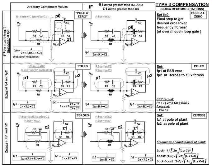
Fig. 15: Type 3 Conventional Operational Amplifier Compensation
... dual role in determining the poles and zeros. So the calculation can become fairly cumbersome and iterative. But a valid simplifying assumption that can be made is that R1 is much greater than R3, and C1 much greater than C3. So the locations of the poles and zeros are, finally, ...
Note that the reference designators of the components have changed in this section for convenience. What we are now calling "R1" was "Rf2" when we previously discussed the voltage divider. Similarly, the gray unnamed resistor in Fig. 15 was previously called "Rf1."
Let us take up a practical example to show how to proceed in designing a feedback loop with this type of compensation.
Example: Using a 300 kHz synchronous buck controller we wish to step down 15 V to 1 V.
The load resistor is 0.2 Ohm (5 A). The ramp is 2.14 V from the datasheet of the part. The selected inductor is 5 µH, and the output capacitor is 330 µF, with an ESR of 48 m-Ohm.
We know that the plant gain at dc for a buck is VIN/VRAMP = 7.009. Therefore, (20 × log) of this gives us 16.9 dB. The LC double pole for a buck is at ...
We want to set the crossover frequency of the open-loop gain at one-sixth the switching frequency, that is, at 50 kHz. Therefore we can solve for the integrator's "RC" by using our previous (simplified) equation ...
However, in all cases, we must ensure that the selected crossover frequency is at least an order of magnitude below the RHP zero (location provided previously)!! Optimizing the Feedback Loop
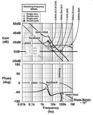
Fig. 16: Plotting the Results for the Type 3 Compensation Example (nonoptimized)
In Fig. 16 we have plotted the results of the previous example, and we can see that though the crossover frequency is high enough, the phase margin is rather too generous.
A very high phase margin may be "very stable," with almost no ringing, but there will be greater undershoot/overshoot.
But what did we expect? Let's analyze this further. For now, let us ignore the high-frequency pole "p2" of the error amplifier. Let us also ignore "p1" since it mutually cancels out with respect to the ESR zero coming from the plant. Therefore the plant just has a double pole at frequency fLC, and this tends to give it the ominous shift of 180° we talked about. But our two single-order zeros from our error amplifier mutually cancel this double pole. So that effectively leaves us with just the pole-at-zero coming from the integrator section of the error amplifier. And like any single pole, this provides a net -90° phase shift to the open-loop characteristics. The phase margin is therefore expected to be 90° short of -180°, that is, 90°.
It’s no surprise we got an actual phase margin of 79° as seen in Fig. 16. The conclusion is that we are certainly very stable, with no possibility of oscillations, but we are also over-damped. We can however accept this as a viable solution too, except perhaps in more critical applications. But if the application is critical, what we would really want to do is to be able to maintain the present crossover frequency of 50 kHz (1/6th of the switching frequency), but to make the phase margin slightly "worse" -- for better transient response.
We should also have realized by now that intuitively, poles are generally responsible for making matters "worse" - since they always introduce a phase lag, leading us closer to the danger level of -180°. On the other hand, zeros boost the phase angle (phase lead), and thereby help increase the phase margin away from the danger level.
Therefore, logically, to decrease the existing phase margin of 79° to say 45°, we need another pole -- that is, to make matters "worse," though in a calculated manner. And in fact, that is what p2 does (we have just not been considering it in our present discussion).
Looking back at our worked example and the resultant gain-phase plots, we realize that the reason its effect at the crossover frequency was minimal was that we had placed it too far out (10 × f_cross). Let us therefore now change its criterion and place it exactly at the crossover frequency. So we now have:+
fp2 = f_cross = 50 kHz
We can guess that the phase shift introduced by a single pole at its resonant frequency is 45°, so the new phase margin should be around 79° - 45° = 34°. We plot the gain-phase plots with this new high-frequency pole criterion (and freshly calculated compensation component values) and we get the curve shown in Fig. 17.
In Fig. 17, we see that the phase margin is now almost exactly 45°. The reason it’s a little more than our initial estimate of 34° (though we desired 45°), is that the crossover frequency has decreased slightly to 40 kHz.
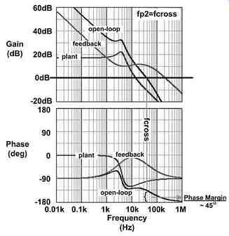
Fig. 17: Plotting the Results for the Type 3 Compensation Example (optimized)
Note that in terms of the asymptotic approximation, the open-loop gain crosses the 0 dB axis with a slope of -1, but then immediately thereafter falls off at a slope of -2. But since the pole is very close to the crossover frequency, the gain in reality falls by 3 dB at this break point (as compared to the asymptotic approximation). So the actual crossover occurs a little earlier. The reason the phase is affected by almost 45° at the crossover frequency is that phase starts changing a decade below where the pole really is.
It can therefore be shown that by trying to place the high-frequency pole exactly at the crossover frequency, the crossover frequency itself shifts downward by almost exactly 20%. So the corollary to that is - if we are starting a compensation network design in which we are going to use the high-frequency pole in this manner, we should initially target a crossover frequency about 20% higher than we actually desire (and get).
Note that engineers use various "tricks" to improve the response further. For example, they may "spread" the two zeros symmetrically around the LC double pole (rather than coinciding with it). One reason to put a zero (or two) slightly before the LC pole location is that the LC pole can produce a very dramatic 180° phase shift, and this can sometimes lead to conditional stability. So the zero absorbs some of that "abruptness" in a sense.
Conditional stability is said to occur if the phase gets rather too close to the -180° danger level at some frequency. Though oscillations don’t normally occur at this point, simply because the gain is high (crossover is not taking place at this location), under large-signal disturbances, the gain of the converter can suddenly fall momentarily toward 0 dB, thus increasing the chance of instability. For example, if there is a very large change in line and load, the error amplifier output may "rail," that is, reach a value close to its internal supply rails. Its output transistors may then saturate, taking a comparatively long time to recover and respond. So the gain would have effectively decreased suddenly, and it could end up crossing the 0 dB axis at the same location where the phase angle happens to be -180° - and that would meet the criterion for full-blown instability.
Input Ripple Rejection
Why are we interested in maximizing the open-loop gain T = GH anyway? Because it can be shown that the effect of line and load variations on the output is decreased by virtually the same factor 'T.' For example, looking at the earlier equation, we see that the line-to-output transfer function for the buck is the same as its control-to-output transfer function, except that the VIN/VRAMP factor is replaced by D. So for example, if VRAMP = 2.14 V, and D = 0.067 (as for 1 V output from a 15 V input), then the control-to-output gain at low frequencies is
...and the line-to-output transfer gain at low frequencies is therefore:
20 × log (D) = 20 × log (0.067) =-23.5 dB
The latter represents attenuation, since the response at the output is less than the disturbance injected into the input. But both these are without feedback considered (or with the error amplifier set to a gain of 1, and with no capacitors used anywhere in the compensation).
So when feedback is present ("loop closed"), it can be shown by control loop theory that the line-to-output transfer function changes to line-to-output with feedback = × line-to-output without feedback
… where T = GH.
Since T (the open-loop transfer function) at low frequencies is very large, so T + 1 ˜ T. Further, since 20 × log (1/T) =-20 × log (T), we conclude that at low frequencies, the additional attenuation provided when the loop is closed is equal to the open-loop gain. For example if the open-loop gain at 1 kHz is 20 dB, it attenuatesa1kHz line disturbance by an additional 20 dB - over and above the attenuation already present without feedback considered.
Let's conduct a more detailed analysis. Suppose we are interested in attenuating the 100 Hz (low-frequency) ripple component of the input voltage in an off-line power supply to a very small value. If our crossover frequency is 500 kHz, then by using the simple relationship derived in Fig. 6, we can find the open-loop gain at 100 Hz (here we are assuming we carried out the recommended compensation scheme, which leaves us effectively with only a pole-at-zero response in the open-loop gain). So the gain at 100 Hz is:
Open-Loop-Gain100Hz = f_cross
100Hz = 500
Expressed in dB, this is 20 × log
_ Open-Loop-Gain100Hz
= 20 × log (500) = 54 dB
So the additional attenuation is 54 dB here. But we already had |20 × log (D)|= 23.5 dB of attenuation. So by introducing feedback, the total attenuation of the 100 Hz input ripple component has increased to 54 + 23.5 = 77.5 dB. This is equivalent to a factor of 1077.5/20 = 7500. So if, for example, the low-frequency ripple component at the input terminals was ±15 V, then the output will see only ±15/7500 =±2 mV of disturbance.
Load Transients
Suppose we suddenly increase the load current of a converter from 4 A to 5 A. This is a "step load" and is essentially a nonrepetitive stimulus. But by writing all the transfer functions in terms of s rather than just as a function of j?, we have created the framework for analyzing the response to such disturbances too. We will need to map the stimulus into the s-plane with the help of the Laplace transform, multiply it by the appropriate transfer function, and that will give us the response in the s-plane. We then apply the inverse Laplace transform and get the response with respect to time. This was the procedure symbolically indicated in Fig. 3, and that is what we need to follow here too.
However, we won’t perform the detailed analysis for arbitrary load transients here, but simply provide the key equations required to do so.
The 'output impedance' of a converter is the change in its output voltage due to a (small) change in the load current. With feedback not considered it’s simply the parallel ...
... where R is the load resistance, and L is the actual inductance L for a buck, but is L/(1 - D) / 2 for a boost and a buck-boost. We have taken the three components in parallel as indicated by the symbol "||."
With feedback considered, the output impedance now decreases as follows:
Zout_ with feedback = 1 / 1 + T × Zout_ without feedback
Even without a detailed analysis (using Laplace transform), this should tell us by how much the output voltage will eventually shift (settle down to), if we change the load current.
Type 1 and Type 2 Compensations
In Fig. 18, we have also shown Type 1 and Type 2 compensation schemes (though with no particular strategy in placing the poles and zeros). These are less powerful schemes than Type 3. So whereas Type 3 gives us one pole-at-zero AND 2 poles AND 2 zeros, Type 2 gives us one pole-at-zero AND 1 pole AND 1 zero. Whereas Type 1 gives us ONLY a pole-at-zero (simple integrator).
We know that we always need a pole-at-zero in the compensation, for achieving high dc gain, good dc regulation, and low-frequency line rejection. So the -1 slope coming from the pole-at-zero adds to the -2 slope from the double pole of the LC filter and this gives us a -3 slope - that is if we don't put in any more zeros and poles. But still we want to intersect the 0 dB axis with a -1 overall slope. So that means we definitely need two (single-order) zeros to force the slope to become -1.
Type 2 compensation can also be made to work, because though it provides only one zero, we can use the zero from the ESR of the output capacitor (despite its relative unpredictability).
We remember, in Type 3 we canceled out the ESR zero completely, citing its relative unpredictability. But now we can consider using it to our advantage, if that is indeed possible. Of course, for the Type 2 scheme to work, the ESR zero must be located at a lower frequency than the intended crossover frequency.
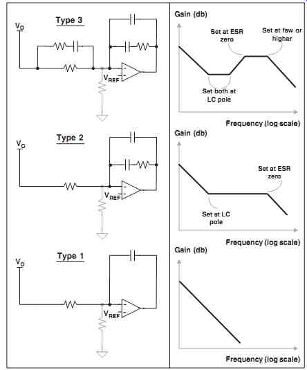
Fig. 18: Type 1, Type 2, and Type 3 Compensation Schemes (poles and zeros
arbitrarily placed and displayed)
Alternatively, we can easily use Type 2 compensation with current mode control, as explained later.
Type 1 compensation provides only a pole-at-zero, and in fact can only work with current mode control (that too with the ESR zero below crossover). Note that it’s just a simple integrator.
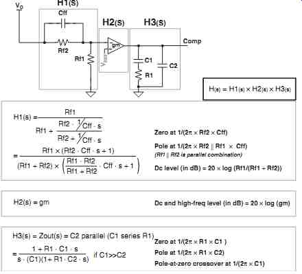
Fig. 19: "Full-blown'' Transconductance Operational Amplifier Compensation
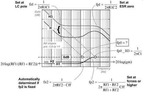
Fig. 20: The Intermediate Feedback Blocks of the Transconductance Op-amp
Transconductance Op-amp Compensation
The final stages of the analysis of voltage mode controlled converters are reserved for the transconductance op-amp. In Fig. 13 we had presented its transfer function rather generically. Now let us consider the details.
We can visualize this feedback stage as a product of three transfer functions, H1, H2, and H3 as shown in Fig. 19. When we plot the separate terms out as in Fig. 20, we see that this looks superficially like Type 3 compensation - but it’s not! Though it provides two zeros and two poles (besides the inevitable pole-at-zero), we see a big difference - especially in the behavior of H1 (the input side). The problem here is that the dc level of H1 is fixed by the resistive divider (now called Rf2 and Rf1). Its high-frequency value is also fixed at 0 (think of the capacitor Cff conducting fully). So along the way, it transits by means of one zero, followed by a pole. But the slope during this transition has to be +1as for any single-order (RC) combination. What all this means is that effectively, if we fix pole fp2 at some frequency, the location of the zero fz2 is automatically defined. There is no flexibility in using this zero and pole pair. For example, if we try to fix both zeros of the overall compensation network at the LC double-pole frequency, the pole fp2 will be literally dragged along with fz2, and so the overall open-loop gain would finally fall at -2 slope again, not at -1 as desired. Therefore, the zero of H1 can only be used if the associated pole fp2 is at or beyond the crossover frequency. Our final strategy for placing the poles and zeros is indicated in Fig. 20.
It actually requires a great deal of mathematical manipulation to solve the simultaneous equations and to come up with component values for a desired crossover frequency.
Therefore, the derivation is not presented here, but the steps are in accordance with the basic math-in-the-log-plane tools presented in Fig. 6. The final equations are presented below, through a numerical example, similar to what we did for Type 3 compensation.
Note: The way we have separated the terms of the transconductance op-amp, the "pole-at-zero" (fp0_H3) seems to be dependent only on C1 (no resistance term). However, we could have also "clubbed" the voltage divider section H1 along with H3 (since these are simply cascaded blocks, in no particular order). Then the "pole-at-zero" would have appeared differently (and also included a resistance term). However, whichever way we proceed, the final result, that is, H, will remain unchanged. In other words, H1, H2, and H3 are just intermediate mathematical constructs in calculating H (with no obvious physical meaning of their own necessarily). That is why the actual pole-at-zero frequency of the entire feedback block is designated as fp0, not fp0_H3.
Example: Using a 300 kHz synchronous buck controller we wish to step down 25 V to 5 V.
The load resistor is 0.2 Ohm (25 A). The ramp is 2.14 V from the datasheet of the part. The selected inductor is 5 µH, and the output capacitor is 330 µF, with an ESR of 48 m-Ohm. The transconductance of the error amplifier is gm = 0.3 (units for transconductance are "mhos," i.e. ohms spelled backwards). The reference voltage is 1 V.
The LC double pole occurs at ...
We have presented the computed gain-phase plots in Fig. 21. We see that we have an adequate 40° of phase margin, and the crossover frequency is 40 kHz. Note that for visual clarity we used a rather small output capacitance and a large ESR for this particular application and power level. And that is why C1 is not very much larger than C2. But the intention was to shift the ESR zero to less than the crossover frequency, just to demonstrate the principle and be able to plot it out easily. However, the equations and above procedure are valid for any output capacitance and ESR. ....
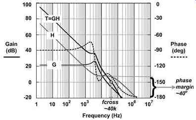
Fig. 21: Plotting the Results of the "Full-blown" Transconductance
Op-amp-based Compensation Example