AMAZON multi-meters discounts AMAZON oscilloscope discounts
..
Feedback Stage Transfer Functions
Let us now lump the entire feedback section, including the voltage divider, error amplifier, and the compensation network. However, depending on the type of error amplifier used, this must be evaluated rather differently. In Fig. 13 we have shown two possible error amplifiers often used in power converters.
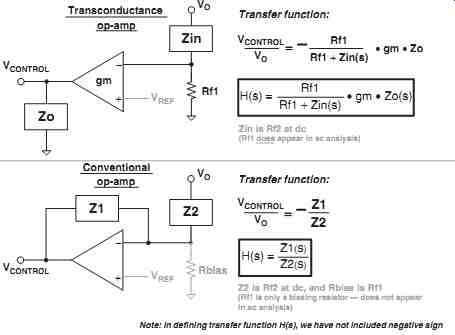
Fig. 13: Generic Representation of Feedback Stages: Note: In defining
transfer function H(s), we have not included negative sign
The analysis for these two cases is as follows:
++ The error amplifier can be a simple voltage-to-voltage amplification device, that is, the traditional "op-amp" (operational amplifier). This type of op-amp requires local feedback (between its output and inputs) to make it stable. Under steady dc conditions, both the input terminals are virtually at the same voltage level. This determines the output voltage setting. But, as discussed previously, though both resistors of the voltage divider affect the dc level of the converter's output, from the ac point of view, only the upper resistor enters the picture. So the lower resistor is considered purely a dc biasing resistor, and therefore we usually ignore it in control loop (ac) analysis.
++ The error amplifier can also be a voltage-to-current amplification device, that is, the "gm op-amp" (transconductance operational amplifier). This is an open-loop amplifier stage with no local feedback - the loop is in effect completed externally, and that again causes the voltages at its input terminals to get equalized (like a regular op-amp). If there is any difference in voltage between its two pins, ?V, it converts that into a current, ?I, flowing out of its output pin (as determined by its transconductance gm = ?I/?V). Thereafter, since there is an impedance Z connected from the output of this op-amp to ground, the voltage at the output pin of this error amplifier (i.e. the voltage across Z - also the control voltage) changes by an amount equal to ?I × Z. For example, in our converter, if VFB (the voltage from the divider, applied to the inverting pin) increases slightly above VREF, this will cause the op-amp to source less current. That will decrease the control voltage (across Z) and so the duty cycle will decrease. Ultimately, because of the high gain, the system again settles down only when the voltages on the input pins of the op-amp become virtually the same. For the gm op-amp, both Rf2 and Rf1 enter into the ac analysis, because together they determine the error voltage at the pins, and therefore the current at the output of the op-amp. Note that the divider can in this case be treated as a simple (step-down) gain block of Rf1/(Rf1 +Rf2), cascaded with the op-amp stage that follows.
Note: We may have wondered - why do we always use the inverting terminal of the error amplifier for applying the feedback voltage? The intuitive reason for that is that an inverting op-amp has a dc gain of Rf/Rin, where Rf is the feedback resistor (from the output of the op-amp to its negative input terminal), and Rin is the resistor between its inverting terminal and the input voltage source. So the output of an inverting op-amp can be made smaller than its input, if so desired (i.e. gain <1). Whereas, a noninverting op-amp has a dc gain of 1+ (Rf/Rin), where Rin in this case is the resistor between its inverting terminal and ground.
So its output will always be greater than its input (gain >1). This restriction on the dc gain has been known to cause some strange and embarrassing situations in the field, especially under certain abnormal conditions.
Therefore, a non-inverting error op-amp is generally not favored.
Lastly, note that by just using an inverting error amplifier, we have in effect also applied a -180° phase shift "right off the bat"! We will see in the following section, that this increases the possibility of oscillations by itself.
Closing the Loop
We’re now in a position to start tying all the loose ends together! For each of the three topologies, we now know both the forward transfer function G(s) (control-to-output) and also the feedback transfer function H(s). Going back to the basic equation for the closed-loop transfer function,
(closed-loop transfer function)
... we see that it will "explode" if...
But G(s)H(s) is simply the transfer function for a signal going through the G(s) block, and then through the H(s) block, that is, the open-loop transfer function. We know that the gain is the magnitude of the transfer function (using s = j?), and its phase angle is its argument. Let us calculate what these are for the transfer function of -1 above.
Note: When doing the tan-1 operation, we may often need to visualize where the number is actually located in the complex plane. For example, in this case, tan of 0° and tan of 180° are both zero, and we wouldn't have known which of these angles is the right answer -- unless we visualized the number in the complex plane. In our case, since the number was minus 1, we correctly placed it at 180° instead of 0°.
So we see that the system is unstable if a disturbance (of certain frequency) goes through the plant and feedback blocks, and returns at 180° angle, with the same magnitude.
The summing block that follows has one negative and one positive input, since it represents a negative feedback system. This implies that another 180° shift will occur after the signal leaves the H block. So we conclude that in general, a system would be unstable if a disturbance goes around the loop and comes back to the same point, with the same magnitude and the same phase.
In a typical gain vs. frequency plot, we will see that a gain of 1 usually occurs at only one specific frequency, and this is called the 'crossover' frequency. Beyond this point the gain becomes less than 1 (i.e. below the 0 dB axis).
The stability criterion is therefore equivalent to saying that the phase shift (of the open-loop transfer function) should not be equal to 180° (or -180°) at the crossover frequency. But we need to ensure a certain margin of safety - in terms of the degrees of phase angle at the crossover frequency required to prevent this from happening. This safety margin is called the 'phase margin. '
Note that the possibility of instability applies only at the crossover frequency. For example, it surprisingly doesn't matter even if the response somehow manages to come back larger than the stimulus itself, even at the same phase angle - that does not cause instant instability, simply because it can be shown this particular vector condition can't support any further increase in the amount of disturbance.
How much phase margin is enough? In theory, even an overall phase shift of -179° (i.e. a phase margin of 1°) would not produce full instability - though there would certainly be a lot of ringing at every transient, and at best it would be very, very, marginally stable. But component tolerances, temperature variations, and even small changes in the application conditions can change the loop characteristics significantly, ushering in full-blown instability.
It’s generally recommended that the phase lag introduced by the successive G and H blocks be about 45° short of -180° - that is, an overall phase lag of -135°. That gives us a phase margin of 45°. On the other hand, a phase margin of, say, 80° is certainly very stable, but is also usually not very desirable. Under transients, though there is no ringing (after the
first overshoot or undershoot), the correction is too slow, and the thus the amount of overshoot/undershoot can become quite significant. A phase margin of 45° would generally be seen to cause just one or two cycles of ringing, and the overshoot/undershoot would also be minimal.
Note: Under very large line or load steps, we will actually no longer be operating in the domain of the "small-signal" analysis which we have been performing so far. In that case, the initial overshoot/undershoot at the output is almost completely determined simply by how large a bulk capacitance we have placed at the output. That capacitance is needed to "hold" the output steady, until the control loop can enter the picture and help stabilize the output.
Criteria for Loop Stability
We should remember that phase angle can start changing gradually - starting at a frequency even 10 times lower than where the pole or zero may actually reside. We have also seen that a second-order double-pole (-2 slope with two reactive components) can cause a very sudden phase shift of about 180° at the resonant frequency if the Q is very high.
Therefore, in practice, it’s almost impossible to estimate the phase at a certain frequency, with certainty - nor therefore the phase margin - unless a certain strategy is followed! Therefore, one of the most popular (and simple) approaches to ensuring loop stability is as follows:
++ Ensure that the open-loop gain crosses the 0 dB axis with a -1 slope.
++ We also want to maximize the bandwidth to achieve quick response to extremely sudden load or line transients. By sampling theory, we know that we certainly need to set the crossover frequency to less than half the switching frequency. So, in practice, most designers set the crossover frequency at about one-sixth the switching frequency (for voltage mode control).
++ Ensure that the crossover frequency is well below any troublesome poles or zeros - like the RHP zero in continuous conduction mode (boost and buck-boost - with voltage mode or current mode control), and the "subharmonic instability pole" in continuous conduction mode (buck, boost, and buck-boost - with current mode control). The latter pole is discussed later.
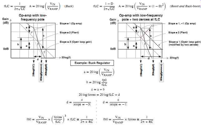
Fig. 14: Calculating the Open-loop Gain and Stabilizing the Loop
Plotting the Open-loop Gain and Phase with an Integrator
We’re interested in plotting the gain and phase of the open-loop transfer function T(s). This is the product of the transfer functions of the G (plant) and H (feedback) blocks in cascade.
Review the rules presented earlier in the section "mathematics in the log plane." Let us start by taking a typical plant and then following it up with the simple integrator (first described in Fig. 5). On the left-hand side of Fig. 14 we have plotted the plant gain, the gain of the op-amp integrator, and the overall gain. We can see that the latter is simply the sum of the previous gains (when expressed in dB). We also see that the plant gain falls off after its resonant frequency at a slope of -2. But the integrator slope is falling at -1. Therefore the overall (cascaded) slope is -1 before the double pole, and -3 thereafter. That is why we need a "compensation network" around the error amplifier, to meet our simple loop design strategy mentioned in the previous section.
In particular, at lower frequencies we can clearly see that the open-loop gain is offset vertically by an amount equal to the plant gain. If the plant is a buck, then we know its ...
Therefore, if we have a certain crossover frequency, 'f_cross,' in mind, this tells us the 'RC' that the integrator section must have, to make that happen.
However, we still have a problem. Though we can clearly set the open-loop crossover frequency almost where we want, we are still not crossing over with a -1 slope as desired.
Canceling the Double Pole of the LC Filter
In the right-hand side of Fig. 14 we have hypothetically (so far) modified the compensation of the previous section to now include two single-order zeros - placed exactly where the plant's double pole lies - thus effectively canceling the latter out completely. The op-amp still provides the necessary pole-at-zero from its "integrator section," and if extrapolated, this would cross over at fp0 with a slope of -1. But now, with the two-zeros present, the open-loop gain also now falls at a slope of -1 (except for the slight LC peaking along the way). Note that there is a vertical offset between these two curves by an amount equal to the plant gain at low frequencies (which we already know from above).
Therefore we can easily apply the equations given in the lower half of Fig. 6.
Simplifying, we will get the following relationship between 'f_cross' (the crossover frequency of the open-loop gain) and 'fp0'.
This equation therefore connects the desired crossover frequency with the required 'RC' product of the integrator section of the op-amp. We can thus adjust the RC to get the required crossover.
Note that for a boost or buck-boost, the only change required in the above analysis is ....
Our compensation analysis seems complete. However, there is one last complication still remaining. We may need at least one pole from our compensation network. This is for canceling out the 'ESR zero' coming from the output capacitor. We have been ignoring this particular zero so far, but it’s time to take a look at it now.