AMAZON multi-meters discounts AMAZON oscilloscope discounts
..
The Voltage Divider
The output VO of the power supply first goes to a voltage divider. Here it’s in effect, just stepped-down, for subsequent comparison with the reference voltage 'VREF.' The comparison takes place at the input of the error-amplifier, which is usually just a conventional op-amp (voltage amplifier).
We can visualize an ideal op-amp as a device that varies its output so as to virtually equalize the voltages at its input pins. Therefore in steady state, the voltage at the node connecting Rf2 and Rf1 (see "divider" block in Fig. 10) can be assumed to be (almost) equal to VREF.
Assuming that no current flows out of (or into) the divider at this node, using Ohm's law ...
So this tells us what ratio of the voltage divider resistors we must have, to produce the desired output rail.
Note however, that in applying control loop theory to power supplies, we are actually looking only at changes (or perturbations), not the dc values (though this was not made obvious in Fig. 9). It can also be shown that when the error amplifier is a conventional op-amp, the lower resistor of the divider, Rf1, behaves only as a dc biasing resistor and does not play any (direct) part in the ac loop analysis.
Note: The lower resistor of the divider, Rf1, does not enter the ac analysis, provided we are considering ideal op-amps. In practice, it does affect the bandwidth of a real op-amp, and therefore may on occasion need to be considered.
Note: If we are using a spreadsheet, we will find that changing Rf1 does in fact affect the overall loop (even when using conventional op-amp-based error amplifiers). But we should be clear that that is only because by changing Rf1, we have changed the duty cycle of the converter (its output voltage), which thus affects the plant transfer function. Therefore, in that sense, the effect of Rf1 is only indirect. We will see that Rf1 does not actually enter into any of the equations that tell us the locations of the poles and zeros of the system.
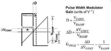
Fig. 12: Gain of Pulse Width Modulator
Pulse Width Modulator Transfer Function (gain)
The output of the error amplifier (sometimes called "COMP," sometimes "EA-out," sometimes "control voltage") is applied to one of the inputs of the pulse width modulator ('PWM') comparator. On the other input of this comparator, we have an applied sawtooth voltage ramp - either internally generated from the clock when using "voltage mode control," or derived from the current ramp when using "current mode control." Thereafter, by normal comparator action, we get pulses of desired width, with which to drive the switch.
Since the feedback signal coming from the output rail of the power supply goes to the inverting input of the error-amplifier, if the output is below the set regulation level, the output of the error amplifier goes high. This causes the pulse width modulator to increase pulse width (duty cycle) and thus try and make the output voltage rise. Similarly, if the output of the power supply goes above its set value, the error amplifier output goes low, causing the duty cycle to decrease. See the upper half of Fig. 11.
As mentioned previously, the output of the pulse width modulator stage is duty cycle, and its input is the 'control voltage' or the 'EA-out.' So, as we said, the gain of this stage is not a dimensionless quantity, but has units of 1/V. From Fig. 12 we can see that this gain is equal to 1/VRAMP, where VRAMP is the peak-to-peak amplitude of the ramp sawtooth.
Voltage Feedforward
We had also mentioned previously, that when there is a disturbance, the control does not usually know beforehand how much duty cycle correction to apply. In the lower half of Fig. 11, we have described an increasingly popular technique being used to make that really happen (when faced with line disturbances). This is called input-voltage/line feedforward, or simply "feedforward."
This technique requires that the input voltage be sensed, and the slope of the comparator sawtooth ramp increased, if the input goes up. In the simplest implementation, a doubling of the input causes the slope of the ramp to double. Then, from Fig. 11, we see that if the slope doubles, the duty cycle is immediately halved - as would be required anyway if the input to a buck converter is doubled. So the duty cycle correction afforded by this "automatic" ramp correction is exactly what is required (for a buck, since its duty cycle D = VO/VIN). But more importantly, this correction is virtually instantaneous - we didn't have to wait for the error amplifier to detect the error on the output (through the inherent delays of its RC-based compensation network scheme), and respond by altering the control voltage. So in effect, by input feedforward, we have bypassed all major delays, and so line correction is virtually instantaneous (i.e. "perfect" rejection of disturbance).
We just stated that in its simplest form, feedforward causes the duty cycle to halve if the input doubles. Let us double-check that that is really what is required here. From the dc input-to-output transfer function of a buck topology, ...
Therefore, on doubling the input,...
... which is what we are doing anyway, through feedforward. So, we can see that this simple feedforward technique will work very well for a buck. However, for a boost or a buck-boost, the duty-cycle-to-input proportionality is clearly not going to be the best answer.
Using voltage feedforward to produce automatic line rejection is clearly applicable only to voltage mode control. However, the original inspiration for this idea came from current mode control. But in current mode control, the ramp to the PWM comparator is being generated from the inductor current waveform. In a buck topology for example, the slope of the inductor current up-ramp is equal to (VIN - VO)/L. So if we double the input voltage, we don’t end up doubling the slope of the inductor current. Therefore, neither do we end up halving the duty cycle. But in fact, we need to do exactly that, if we are looking for complete line rejection (from D = VO/VIN). In other words, voltage mode control with feedforward in fact provides better line rejection than current mode control (for a buck).
Power Stage Transfer Function
The power stage formally consists of the switch plus the (equivalent) LC filter. Note that this is just the plant minus the pulse width modulator. (see Fig. 10).
We had indicated previously that whereas in a buck, the L and C are really connected to each other at the output (as drawn in Fig. 10), in the remaining two topologies they are not.
However, the small-signal (canonical) model technique can be used to transform these latter topologies into equivalent ac models - in which, for all practical purposes, a regular LC-filter does appear after the switch, just as for a buck. With this technique, we can then justifiably separate the power stage into a cascade of two separate stages (as for a buck):
++ A stage that effectively converts the duty cycle input (coming from the output of the PWM stage), into an output voltage
++ An equivalent post-LC filter stage, that takes in this output and converts it into the output rail of the converter With this understanding, we can build the final transfer functions presented in the next section.
Plant Transfer Functions of All the Topologies
Let us discuss the three major topologies separately here. Note that we are assuming voltage mode control and continuous conduction mode. Further, the "ESR zero" is also not included here (introduced later).
Buck Converter
Control-to-Output Transfer Function
The transfer function of the plant is also called the 'control-to-output transfer function' (see Fig. 10). It’s therefore the output voltage of the converter, divided by the 'control voltage' (EA-out). We’re of course talking only from an ac point of view, and are therefore interested only in the changes from the dc-bias levels.
The control-to-output transfer function is a product of the transfer functions of the PWM, the switch and the LC filter (since these are cascaded stages). Alternatively, the control-to-output transfer function is a product of the transfer functions of the PWM stage and the transfer function of the 'power stage'.
We already know from Fig. 12 that the transfer function of the PWM stage is equal to the reciprocal of the amplitude of the ramp. And as discussed in the previous section, the power stage itself is a cascade of an equivalent post-LC stage (whose transfer function is the same as the passive low-pass second-order LC filter we discussed previously), and a stage that converts the duty cycle into an output voltage. We’re interested in finding the transfer function of this latter stage.
The question really is - what happens to the output when we perturb the duty cycle slightly (keeping the input to the converter, VIN, constant)? Here are the steps for a buck:
Therefore, differentiating...
And this is the required transfer function of the intermediate duty-cycle-to-output stage! Finally, the control-to-output transfer function is the product of three (cascaded) transfer functions, that is, it becomes ...
Alternatively, this can be written as ...
Line-to-output Transfer Function
Of primary importance in any converter design is not what happens to the output when we perturb the reference (which is what the closed loop transfer function really is), but what happens at the output when there is a line disturbance. This is often referred to as 'audio susceptibility' (probably because early converters switching at around 20 kHz would emit audible noise under this condition).
The equation connecting the input and output voltages is simply the dc input-to-output transfer function, that is,...
So this is also the factor by which the input disturbance first gets scaled, and thereafter applied at the input of the LC filter. But we already know the transfer function of the LC low-pass filter. Therefore, the line-to-output transfer function is the product of the two, that is, ...where R is the load resistor (at the output of the converter).
Alternatively, this can be written as ...
Boost Converter
Control-to-Output Transfer Function
Proceeding similar to the buck, the steps for this topology are ...
Note that we have included a surprise term in the numerator above. By detailed modeling it can be shown that both the boost and the buck-boost have such a term. This term represents a zero, but a different type to the "well-behaved" zero discussed so far (note the sign in front of the s-term). If we consider its contribution separately, we will find that as we raise the frequency, the gain will increase (as for a normal zero), but simultaneously, the phase angle will decrease (opposite to a "normal" zero, more like a "well-behaved" pole).
We will see later that if the overall open-loop phase angle drops sufficiently low, the converter can become unstable because of this zero. That is why this zero is considered undesirable. Unfortunately, it’s virtually impossible to compensate for (or "kill") by normal techniques. The only easy route is literally to "push it out" - to higher frequencies where it can't affect the overall loop significantly. Equivalently, we need to reduce the bandwidth of the open-loop gain plot to a frequency low enough that it just doesn't "see" this zero. In other words, the crossover frequency must be set much lower than the location of this zero. ...
The name given this zero is the 'RHP zero' , as indicated earlier -- to distinguish it from the "well-behaved" (conventional) left-half-plane zero. For the boost topology, its location can be found by setting the numerator of the transfer function above to zero, that is, s × (L/R) = 1.
So the frequency location of the boost RHP zero is ....
Note that the very existence of the RHP zero in the boost and buck-boost can be traced back to the fact that these are the only topologies where an actual LC post-filter doesn't exist on the output. Though, by using the canonical modeling technique, we have managed to create an effective LC post filter, the fact that in reality there is a switch/diode connected between the actual L and C of the topology, is what is ultimately responsible for creating the RHP zero.
Note: Intuitively, the RHP zero is often explained as follows - if we suddenly increase the load, the output dips slightly. This causes the converter to increase its duty cycle in an effort to restore the output.
Unfortunately, for both the boost and the buck-boost, energy is delivered to the load only during the switch off-time. So, an increase in the duty cycle decreases the off-time, and there is now, unfortunately, a smaller interval available for the stored inductor energy to get transferred to the output. Therefore, the output voltage, instead of increasing as we were hoping, dips even further for a few cycles. This is the RHP zero in action. Eventually, the current in the inductor does manage to ramp up over several successive switching cycles to the new level consistent with the increased energy demand, and so this strange situation gets corrected - provided full instability has not already occurred!
Line-to-output Transfer Function
Note that the plant and line transfer functions of all the topologies don’t depend on the load current. That is why gain-phase plots (Bode plots) don’t change much if we vary the load current (provided we stay in CCM).
Note also that so far we have ignored a key element of the transfer functions -the ESR of the output capacitor. Whereas the DCR usually just ends up decreasing the overall Q (less "peaky" at the second-order (LC) resonance), the ESR actually contributes a zero to the open-loop transfer function. Because it affects the gain and the phase significantly, it usually can't be ignored - certainly not if it lies below the crossover frequency (at a lower frequency).