AMAZON multi-meters discounts AMAZON oscilloscope discounts
..
Simpler Transconductance Op-amp Compensation
There is a practical difficulty involved in using the "full-blown" transconductance op-amp compensation scheme discussed above - because the pole and zero from H1 are not independent. They will even tend to coincide if say Rf2 is much smaller than Rf1 (i.e. if the desired output voltage is almost identical to the reference voltage). In that case, the pole and zero coming from H1 will cancel each other out completely. Therefore, we can't proceed anymore, because we were counting on the zero from H1 to change the open-loop gain from -2, to -1, "just in time" before it crossed over.
But there is one other available zero that we can perhaps use -- coming from H3.
Unfortunately, we have used that up already to cancel part of the LC double pole. (Note that if we hadn't done that, then along with the -1 slope imparted to it by the integrator section (pole-at-zero), the open-loop gain would have had a slope of -3 after its LC double pole location). Therefore to correct the open-loop gain slope from -2to -1, we now must use the only other available zero - the ESR zero, which we had actually canceled out deliberately by a pole in the "full-blown" compensation scheme described previously. But if we do that, we no longer need fp1, or C2. So we are left with the simple transconductance stage shown in Fig. 22. The equations for this, based on the new strategy, are presented in the following example.
Example: Using a 300 kHz synchronous buck controller we wish to step down 25 V to 5 V.
The load resistor is 0.2 Ohm (25 A). The ramp is 2.14 V from the datasheet of the part. The selected inductor is 5 µH, and the output capacitor is 330 µF, with an ESR of 48 m-Ohm. The transconductance of the error amplifier is gm = 0.3 (mhos), and the reference voltage is 1 V.
The LC double pole occurs at ...
We choose our target crossover frequency "f_cross" as 100 kHz.
The crossover of the feedback gain (H) occurs at a frequency fp0 ...
We have presented the computed gain-phase plots in Fig. 22. We see we have a generous 78° of phase margin and a crossover frequency of 100 kHz. Based on the logic presented for the Type 3 compensation scheme (nonoptimized case, see section "optimizing the feedback loop"), the phase margin in this case is also expected to be around 90°.
Here too, one way to reduce the phase lag (if so desired) is to reintroduce the pole fp1 from H3 - by reintroducing C2 (as in Fig. 19). So we can then set the position of this new pole at the crossover frequency, for best effect. The value for C2 required for that is ...
Note that by reintroducing C2, the computed crossover again occurs slightly earlier (by about 20%) - at around 80 kHz, instead of 100 kHz. The phase margin is now 36° (closer to the optimal).
Also note that for this simpler compensation scheme to work, the ESR zero must lie between the LC pole frequency and the selected crossover frequency.
As before, for a boost or buck-boost, the only change required in the preceding analysis is ...
However, we must also always ensure that the selected crossover frequency is at least an order of magnitude below the RHP zero!!
Compensating with Current Mode Control
The plant transfer functions presented earlier were only for voltage mode control. In current mode control, the ramp to the pulse width (duty cycle) modulator is derived from the ....inductor current. It can be shown that in the process, the inductor effectively goes "out of the picture" and so there is no double LC pole anymore. So the compensation is supposedly simpler, and the loop can be made much faster. But the actual mathematical modeling of current mode control has proven extremely challenging - mainly because there are now two feedback loops in action - the normal voltage feedback loop, and a current feedback loop.
Various researchers have come up with different approaches, but even as of now, they don't seem to agree with each other completely.
However everyone does seem to agree that current mode control alters the poles of the system (as compared to voltage mode control), but the zeros are unchanged. So the boost and the buck-boost still have the same RHP zero, as we discussed earlier. And care is still needed to ensure that the RHP zero is at a much higher frequency than the chosen crossover frequency.
As mentioned, in current mode control, the ramp to the PWM comparator is derived from the inductor current. Actually, the most common way of producing the ramp is to simply sense the forward drop across the mosfet (or of course by using an external sense resistor in series with it). This small sensed voltage is then amplified by a current sense amplifier to get the voltage ramp, which is then applied to the PWM comparator. At the other pin of the PWM comparator, we have the output of the error amplifier (control voltage). Since the ramp itself gets terminated at the exact moment when it reaches the control voltage level, in effect, we end up regulating the peak of the inductor current ramp. That is why it’s often said that a converter with current mode control behaves like a current source.
The inductor/switch current ramp is obviously proportional to the voltage ramp at the PWM comparator. So the voltages and currents can be converted into each other through the use of the 'transfer resistance' V/I, as defined in Fig. 23. Therefore we realize that we can look at the overall effect either in terms of currents, or in terms of the voltages - as shown in Fig. 24. We will see that 'slope compensation' too (discussed below) can be expressed either as a certain A/s or as V/s. These are equivalent ways of talking about the same thing, and they are proportional to each other, through the transfer resistance RMAP.
One of the subtleties of current mode control is that (for all the topologies) we need to add a small ramp to the comparator ramp. This is called slope compensation. Its purpose is to prevent an odd artifact of current mode control called subharmonic instability. Subharmonic instability usually shows up as alternate wide and narrow switching pulses. We also discover that the transient response is severely degraded. A bench measurement of a converter that is currently exhibiting this strange pulsing pattern will give us a Bode plot that does not resemble anything we may have been expecting. For one, there is no way to know what the phase margin is.
For subharmonic instability to occur, two conditions have to be met simultaneously - the duty cycle should be close to or exceed 50%, and simultaneously, we should be in CCM (continuous conduction mode). Note that the propensity to enter this state increases as the duty cycle increases (input lowered). So we should always try to rule out this possibility at VINMIN. We could certainly avoid this problem altogether, by choosing DCM (discontinuous conduction mode). But otherwise, in CCM, slope compensation is the recognized sure-fix.
Though it’s interesting to note that by applying slope compensation, we are in effect blending a little voltage mode control with current mode control. In fact, it’s equivalent to taking the ramp generated from the switch/inductor current, and adding a small fixed voltage ramp to it. Or we can do what is more common - modifying the control voltage as shown in Fig. 24.

Fig. 23: How the "Transfer Resistance" Maps the Current in
the Switch, into a Voltage Sawtooth at the Comparator Input
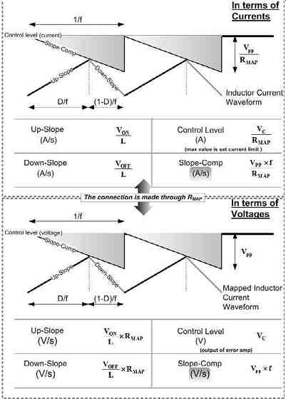
Fig. 24: Slope Compensation Can Be Expressed Either in Terms of Amperes/Second
or as Volts/Second, through the Use of the Transfer Resistance
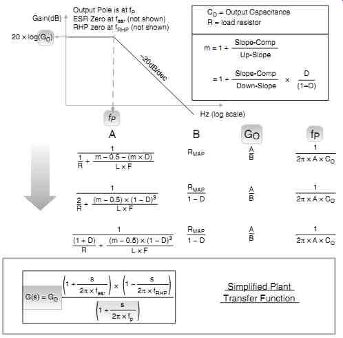
Fig. 25: Simplified Plant Transfer Function for Current Mode Control
If we take the Bode plot of any current mode controlled converter (one that has not yet entered this wide-narrow-wide-narrow state), we will discover an unexplained peaking in the gain plot, at exactly half the switching frequency. This is the "source" of subharmonic instability. Because, though this point is much past the crossover frequency, it’s potentially dangerous because of the fact that if it peaks too much, it can end up intersecting the 0 dB axis again - which we know is one of the prescriptions for full instability.
Subharmonic instability is nowadays being modeled as a pole at half the switching frequency. Note that in any case we never consider setting the crossover frequency higher than half the switching frequency. So in effect, this subharmonic pole will always occur at a frequency greater than the crossover frequency. However, we also realize that its effect on the phase angle may start at a much lower frequency.
The original models for current mode control did not predict this half-switching-frequency peaking (i.e. subharmonic instability). But it has been well known that we need to set a minimum amount of slope compensation - the value of which depends on the slopes of the up-ramp and down-ramp of the inductor current. But the criteria used for setting the precise amount of slope compensation, have been slightly differing. Our approach, outlined later, is based on more recent trends.
The subharmonic pole peaking is akin to the double-pole response of an LC filter. So it, too, has a certain "Q", which depends on the slopes of the inductor current, and the applied slope compensation. If the applied slope compensation is too low, the Q will increase, unless we increase the inductance (to decrease the slopes of the inductor current correspondingly).
In effect, this means we need a certain minimum inductance for a given slope compensation, to remain stable. Alternatively, we need a minimum slope compensation for a given inductance, to remain stable. However, slope compensation, the way it’s commonly applied, affects the peak current limit too, and that can affect the output power capability of the converter. We have to be careful about that too. In general, we should check that we are being able to meet the required output power, at both ends of the input voltage range.
So how much of slope compensation should we really apply? In the section on DC-DC converter design, equations for the minimum inductance were provided. These were actually based on ensuring that Q never exceeds a value of 2 - that value in turn being based on various bench measurements and data, using typical dc-dc converters. A smaller value of Q will certainly be more "safe", but it will require a larger inductor. A large value of Q will lead to subharmonic instability. Hence Q = 2 is normally a good compromise, but it’s prudent to confirm the resulting choice of inductor on the bench, on a case-by-case basis.
The design equations presented for the compensation network below, are based on the simpler model from Middlebrook. But they give a good match with far more elaborate models, provided we realize that:
++ We need to ensure that the RHP zero is much higher than the crossover frequency.
++ The half-switching-frequency pole is also higher than the crossover frequency.
++ In addition, the half-switching-frequency pole is sufficiently "damped" - by introducing the right amount of minimum inductance vis-à-vis the applied slope compensation (or the appropriate amount of slope compensation, based on the desired or optimum value of inductance - as For example for a current ripple ratio of 0.4).
Note that in our presentation, summarized graphically in Fig. 25, we are even ignoring some other poles from Middlebrook's original model, on the grounds that they usually fall well outside the crossover frequency, and therefore are of little practical interest.
In our simplified model, we are thus left with only a single pole in the plant transfer function for all the topologies. This pole comes from the output capacitor and the load resistor (the "output pole"). When we combine it with the inevitable pole-at-zero (from the integrator section of the op-amp), the overall (open-loop) gain will fall with a slope of -2 (after the output pole location). Therefore, we need just one single-zero to cancel part of this slope out, and finally get a -1 slope with which to cross over as desired. Further, this single zero can either be deliberately introduced using Type 2 compensation (in which case we could use its available pole to cancel out the ESR zero) - or we could simply rely on the naturally occurring ESR zero. In the latter case, we would need to ensure that the ESR zero is at a frequency lower than the crossover frequency. That could indirectly force us to move the crossover frequency out to a higher frequency (but without getting too close to the other trouble spots mentioned above). And if we can do that, we may be able to use just a Type 1 compensation scheme - because now we don't need even a single pole in our compensation, other than the inevitable pole-at-zero.
The design equations and steps for the transconductance op-amp are as follows (see Fig. 26).
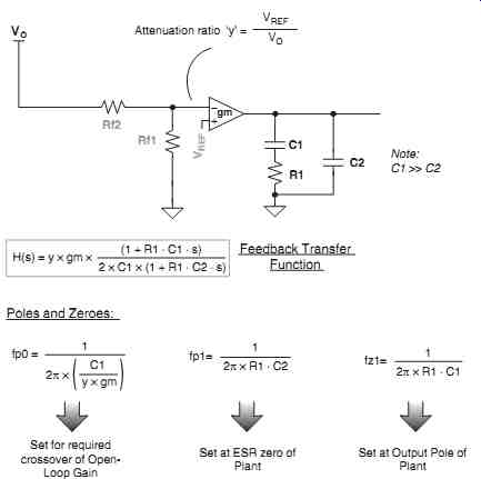
Fig. 26: Transconductance Op-amp for Current Mode Control --- Set for
required crossover of Open Loop Gain -- Set at ESR zero of Plant --- Set
at Output Pole of Plant --- Feedback Transfer Function
1. Choose a crossover frequency 'f_cross.' Although we would like to typically target one-third the switching frequency, we must manually confirm that this frequency is significantly below the location of the RHP zero (the equations for the RHP zero were presented earlier, and they still apply here).
2. We realize that, once again, while plotting the open-loop gain, the gain of the integrator will shift vertically by the amount GO (dc gain of plant). Therefore, using the simple rule in the lower half of Fig. 6, we can find the required fp0 that will ...
The design equations and steps for the conventional op-amp are as follows (see Fig. 27).
1. Choose a crossover frequency 'f_cross.' Although we would like to target one-third the switching frequency if possible, we must manually confirm that this frequency is significantly below the location of the RHP zero. The equations for the RHP zero were presented earlier, and they still apply here.
2. We realize that once again, while plotting the open-loop gain, we will find that the gain of the integrator will effectively shift vertically by the amount GO (dc gain of plant). Therefore, using the simple rule in the lower half of Fig. 6, we can find the required fp0 that will produce the desired crossover frequency (of the open-loop gain). So ...
The above design procedure is the same for all the topologies. We just have to use the appropriate row of the table provided inside Fig. 25. Note that for all the topologies, the "L" used is now the actual inductance of the converter (not the "equivalent" inductance of the canonical model).
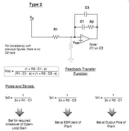
Fig. 27.