AMAZON multi-meters discounts AMAZON oscilloscope discounts
.The three-phase induction motor is probably the most important prime mover for integral-horsepower industrial applications. For the same weight, the rating of a single- phase induction motor is only about 60 percent that of the polyphase machine. Both efficiency and power factor are lower in single-phase motors. However, the three-phase induction motor has often exasperated the application engineer because of its resistance to speed control. Some extension of speed control is provided by the wound-rotor types, but the range is not competitive with that available from dc motors. “If only we could vary the applied frequency,” was a remark often made in the era before solid state. Of course, in some implementations, the frequency was made variable by the use of another motor/alternator set. Such strategy is obviously not economical.
The design of an adjustable frequency, three-phase supply is not difficult if a compromise is made with regard to waveshape. Although a square wave would result in high eddy current and hysteresis losses, it’s still not necessary to synthesize a true sine wave. A stepped waveform consisting of six segments can be created by mixing logic pulses. Such a waveform will have relatively low third-harmonic energy—the chief culprit in eddy current and hysteresis dissipation. The use of digital logic pro vides great simplification because the IC modules displace complex discrete circuits in all three phases.
Another aspect of variable-frequency control is the necessity of changing the motor voltage by the same percentage as the frequency change. In small motors, this basic requirement can be circumvented by inserting resistances in each motor lead. However, such a technique would not be allowable with large motors unless the speed variation were restricted. The use of such resistance also degrades the speed regulation of the motor.
FIG. 7 is a block diagram of a variable-frequency inverter for speed control of a 10-hp three-phase induction motor. Six power channels provide the required sequence of voltage steps needed to develop the quasi-sine wave. This sequence is repeated at 120° intervals in order to supply three-phase energy to the motor.
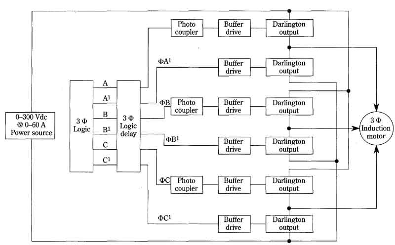
FIG. 7 Block diagram of a variable-frequency inverter for speed control
of 3-phase motors. This one by Delco Electronics.
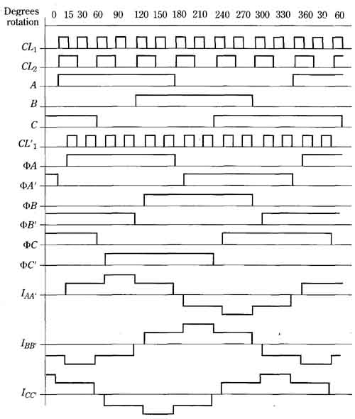
FIG. 8 Logic timing sequence for variable-frequency inverter. Delco
Electronics.
The three-phase wave synthesis imparted by the digital-logic modules commences with the CL pulse train. The subsequent modifications made to these pulses, together with various combining techniques, are illustrated in the logic-timing sequence shown in FIG. 8. Notice that a basic three-phase wave already exits with respect to waves A, B, and C. The circuit points from which these waves are derived in the CMOS logic are designated in FIG. 9. Flip-flops FF102, FF103, and FF104 are connected as a three-bit shift register. Notice that the shift register provides complement waves A’, B’, and C’ as well. These complement waves are used in the building- block process to modify the original ABC three-phase waves. One desired modification is a reduction in the half-wave duty cycle to 165° from the normal 180°. As mentioned previously, this prevents simultaneous conduction of power-output stages that are alternating their conduction states. The other desired modification is a very rough simulation of a sine wave. The CL and CL waves are also used here. (Although the stepped waves ‘i ‘BB and I ultimately delivered to the motor could never actually be mis taken for sine waves, they are nearly as suitable for operation of the motor as a true sine wave. Their salient features are the ease with which they are produced iii logic circuits and their reasonably low third-harmonic content.
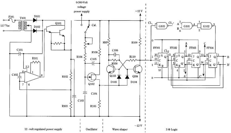
FIG. 9 Voltage-controlled oscillator and 3-phase logic circuit. By
Delco. Labels show: 12-volt regulated power supply; Oscillator; Wave
shaper; 3 -phi Logic.
The NAND gates, G101 and G102, inhibit forbidden-state operation of the shift register. Flip-flop FF101 halves the pulse rate received from the waveshaper, thereby producing wave CL which clocks the modules in the shift register. Finally, an additional clock signal is produced by gate G103. This clock signal, CL is not utilized iii the generation of the basic three-phase waves. Rather, it’s used to clock flip- flops FF411, FF421, FF431, FF451, and FF461, which appear in the schematic diagram of FIG. 10. These flip-flops constitute the 3 Logic Delay shown in the block diagram of FIG. 7. This logic operation imparts the zero-voltage step to each wave m the three-phase sequence.
The basic frequency generated by the voltage-controlled oscillator is 24 times higher than that ultimately delivered to the motor. This is a useful technique of logic synthesis. A low-frequency wave can be constructed from higher-frequency “building blocks.” Although suggestive of Fourier synthesis, the method is simpler—rectangular pulses are manipulated and combined to produce the desired waveform. The pulse synthesis is accomplished in the 3–phi Logic function block of FIG. 7.
An important aspect of the wave shape produced by the logic circuitry is the zero- voltage step. As a consequence of this step, the duration of half cycles applied to the motor is 165°, rather than the usual 180°. This prevents conduction overlap between power-output stages that are turning off and those that are turning on. The function block that produces this zero-voltage step is the 3-phi Logic Delay in FIG. 7. Photo- couplers provide electrical isolation between the three-phase logic circuitry and the motor-drive circuits.
The schematic diagram of FIG. 9 shows the voltage-controlled oscillator and the basic three-phase logic of the inverter. Note that only the charging circuit for Q102, the uni-junction transistor, connects to the external 0-300-volt variable-voltage supply. This allows adjustment of the charging rate of capacitor C 104, and therefore of the pulsing rate of the emitter-base breakdown phenomenon of Q102. As a consequence, the generated frequency and the voltage applied to the motor go up and down together. The near-constant frequency produced by most uni-junction oscillators is due to the fact that the emitter and base circuits connect to the same power source. In this circuit, the interbase voltage is fixed at 12 volts by the internal regulated power supply.
Following the unijunction voltage-controlled oscillator is a driven multivibrator involving transistors Q103 and Q104. This stage processes the oscillator signal to a suitable level and form for actuation of the 3-phi logic modules. The output from Q104 consists of a periodic wave train of rectangular pulses CL These pulses are at half the frequency of those initially generated by the unijunction stage.
Figure 10 is the schematic diagram of the three-phase inverter. This circuitry supplies power to the motor when driven by the signals generated in three-phase logic circuit previously described. Included in this schematic are the delay logic for imparting the zero-voltage step in the motor waveforms, and the photocouplers, which pro vide electrical isolation between low-level logic signals and the power circuits.
The circuit in FIG. 10 is simpler than it looks from an initial inspection. There is much repetition in the circuit configurations. Not only are all circuits for each of the three phases identical, but each of the six power channels contain five Darling- ton output amplifiers connected in parallel. The Darlington amplifiers are type-DTS, triple-diffused silicon units. They have only three terminals, further simplifying the connections as well as reducing the component count. The use of “snubber net works,” exemplified by R512 and C511, is worthy of comment. These RC networks contribute more than mere “despiking” of the waveforms. Actually, they keep the dynamic excursion of Darlington voltage and current within the safe operating area prescribed by the manufacturer. Such load-line “shaping” pays worthwhile dividends in reliability and efficiency.
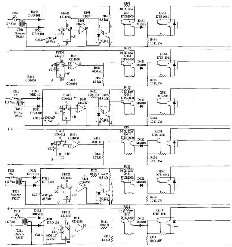
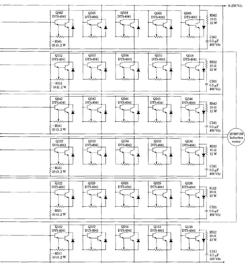
FIG. 10 Schematic diagram of variable-frequency inverter for speed
control of 3-phase motors. from Delco Electronics.
The external dc power supply should have a current capability of about 60 amperes and should permit variation of its output voltage from 0 to 300 volts. Such requirements are best served by a voltage-regulated switching supply, which minimizes power dissipation. An alternative is a simple full-wave power supply with autotransformer control in the power line. A single-phase power line can be used for the dc supply, but three-phase, 60-Hz power would probably be more practical. When the dc supply is adjusted for 250 volts, the motor receives three-phase power at 60 Hz. With 20 volts from the dc supply, the three-phase power supplied to the motor has a frequency of 5 Hz. The speed range corresponding to such a voltage reduction is approximately 1750 RPM to 145 RPM.