AMAZON multi-meters discounts AMAZON oscilloscope discounts
OUTLINE
1. Voltage Regulation (below)
2. Basic Linear Series Regulators (below)
3. Basic Linear Shunt Regulators (below)
4. Basic Switching Regulators (below)
5. Integrated Circuit Voltage Regulators
6. Integrated Circuit Voltage Regulator Configurations Application Activity
GOALS
-- Describe the concept of voltage regulation
-- Describe and analyze the operation of linear series regulators
-- Describe and analyze the operation of linear shunt regulators
-- Discuss the principles of switching regulators
-- Discuss integrated circuit voltage regulators
-- Describe applications of IC voltage regulators
TERMINOLOGY
-- Regulator
-- Line regulation
-- Load regulation
-- Linear regulator
-- Switching regulator
-- Thermal overload
APPLICATION ACTIVITY PREVIEW
In the Application Activity, the dc power supply from Unit 3 is redesigned to produce a regulated variable output voltage from 9 V to 30 V. The company that manufactures the power supply will introduce it as a new line that can be preset to a specified voltage at the factory or adjusted by the customer to any desired value in the output voltage range.
INTRODUCTION
A voltage regulator provides a constant dc output voltage that is essentially independent of the input voltage, output load current, and temperature. The voltage regulator is one part of a power supply. Its input voltage comes from the filtered output of a rectifier derived from an ac voltage or from a battery in the case of portable systems.
Most voltage regulators fall into two broad categories: linear regulators and switching regulators. In the linear regulator category, two general types are the series regulator and the shunt regulator. These are normally available for either positive or negative output voltages. A dual regulator provides both positive and negative outputs. In the switching regulator category, three general configurations are step down, step-up, and inverting.
Many types of integrated circuit (IC) regulators are available. The most popular types of linear regulator are the three-terminal fixed voltage regulator and the three-terminal adjustable voltage regulator. Switching regulators are also widely used. In this Unit, specific IC devices are introduced as representative of the wide range of available devices.
1. VOLTAGE REGULATION
Two basic categories of voltage regulation are line regulation and load regulation. The purpose of line regulation is to maintain a nearly constant output voltage when the input voltage varies. The purpose of load regulation is to maintain a nearly constant output voltage when the load varies.
After completing this section, you should be able to:
-- Describe the concept of voltage regulation
-- Explain line regulation
-- Calculate line regulation
-- Explain load regulation
-- Calculate load regulation
Line Regulation
When the ac input (line) voltage of a power supply changes, an electronic circuit called a regulator maintains a nearly constant output voltage, as illustrated in FIG. 1. Line regulation can be defined as the percentage change in the output voltage for a given change in the input voltage. When taken over a range of input voltage values, line regulation is expressed as a percentage by the following formula:
Line regulation can also be expressed in units of %/V. For example, a line regulation of 0.05%/V means that the output voltage changes 0.05 percent when the input voltage in creases or decreases by one volt. Line regulation can be calculated using the following formula ( Δ means "a change in"):
Line regulation. A change in input (line) voltage does not significantly affect the output voltage of a regulator (within certain limits).
Load Regulation. When the amount of current through a load changes due to a varying load resistance, the voltage regulator must maintain a nearly constant output voltage across the load, as illustrated in FIG. 2.
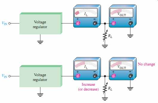
FIG. 2 Load regulation. A change in load current has practically no effect
on the output voltage of a regulator (within certain limits).
Load regulation can be defined as the percentage change in output voltage for a given change in load current. One way to express load regulation is as a percentage change in output voltage from no-load (NL) to full-load (FL).
Alternately, the load regulation can be expressed as a percentage change in output voltage for each mA change in load current. For example, a load regulation of 0.01%/mA means that the output voltage changes 0.01 percent when the load current increases or decreases 1 mA.
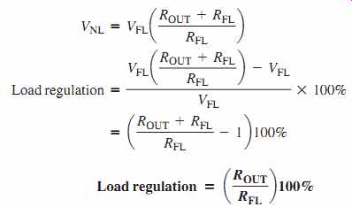
Sometimes power supply manufacturers specify the equivalent output resistance of a power supply (ROUT) instead of its load regulation. Recall that an equivalent Thevenin circuit can be drawn for any two-terminal linear circuit. FIG. 3 shows the equivalent Thevenin circuit for a power supply with a load resistor ROUT. The Thevenin voltage is the volt age from the supply with no load (VNL) and the Thevenin resistance is the specified output resistance, ROUT. Ideally, ROUT is zero, corresponding to 0% load regulation, but in practical power supplies ROUT is a small value. With the load resistor in place, the output voltage is found by applying the voltage-divider rule:
VOUT = VNL [RL/(ROUT + RL)]

FIG. 3 Thevenin equivalent circuit for a power supply with a load resistor.
If we let RFL equal the smallest-rated load resistance (largest-rated current), then the full-load output voltage is (VFL)
VOUT = VNL [RFL/ROUT + RL]
By rearranging and substituting into EQN. 3,
EQN. 4 is a useful way of finding the percent load regulation when the output resistance and minimum load resistance are specified.
SECTION 1 CHECKUP
1. Define line regulation.
2. Define load regulation.
3. The input of a certain regulator increases by 3.5 V. As a result, the output voltage in creases by 0.042 V. The nominal output is 20 V. Determine the line regulation in both % and in %/V.
4. If a 5.0 V power supply has an output resistance of 80 mOhm and a specified maximum output current of 1.0 A, what is the load regulation? Give the result as a % and as a %/mA.
2. BASIC LINEAR SERIES REGULATORS
The fundamental classes of voltage regulators are linear regulators and switching regulators. Both of these are available in integrated circuit form. Two basic types of linear regulator are the series regulator and the shunt regulator.
After completing this section, you should be able to:
-- Describe and analyze the operation of linear series regulators
-- Explain regulating action
-- Determine the closed-loop gain - Determine the output voltage
-- Discuss overload protection
-- Explain constant-current limiting - Determine the maximum load current
-- Discuss fold-back current limiting
A simple representation of a series type of linear regulator is shown in FIG. 4(a), and the basic components are shown in the block diagram in FIG. 4(b). The control element is a pass transistor in series with the load between the input and output.
The output sample circuit senses a change in the output voltage. The error detector com pares the sample voltage with a reference voltage and causes the control element to compensate in order to maintain a constant output voltage. A basic op-amp series regulator is shown in FIG. 5.
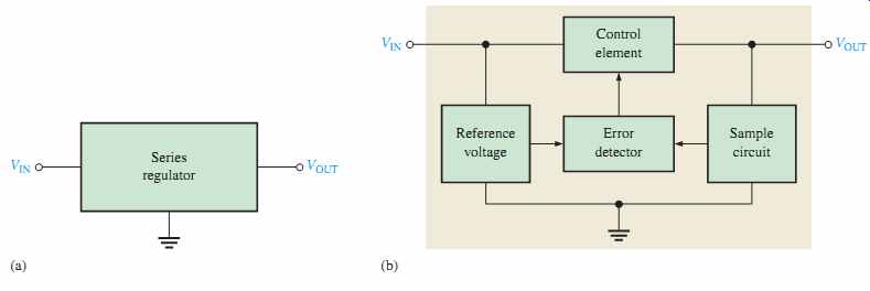
FIG. 4 Simple series voltage regulator and block diagram.
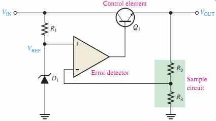
FIG. 5 Basic op-amp series regulator.
Regulating Action
The operation of the series regulator is illustrated in FIG. 6 and is as follows. The resistive voltage divider formed by R2 and R3 senses any change in the output voltage. When the output tries to decrease, as indicated in FIG. 6(a), because of a decrease in Vin or because of an increase in IL caused by a decrease in RL, a proportional voltage decrease is applied to the op-amp's inverting input by the voltage divider. Since the zener diode (D1) holds the other op-amp input at a nearly constant reference voltage VREF, a small difference voltage (error voltage) is developed across the op-amp's inputs. This difference voltage is amplified, and the op-amp's output voltage, increases. This increase is applied to the base of Q1 causing the emitter voltage VOUT to increase until the voltage to the inverting input again equals the reference (zener) voltage. This action offsets the attempted decrease in output voltage, thus keeping it nearly constant. The power transistor, Q1, is usually used with a heat sink because it must handle all of the load current.
The opposite action occurs when the output tries to increase, as indicated in FIG. 6(b). The op-amp in the series regulator is actually connected as a noninverting amplifier where the reference voltage is the input at the noninverting terminal, and the R2/R3 voltage divider forms the negative feedback circuit. The closed-loop voltage gain is:
Acl = 1 + R2/R3
=================
(a) When VIN or RL decreases, VOUT attempts to decrease. The feedback voltage, VFB, also attempts to decrease, and as a result, the op-amp's output voltage VB attempts to increase, thus compensating for the attempted decrease in VOUT by increasing the Q1 emitter voltage.
Changes in VOUT are exaggerated for illustration.
When VIN (or RL) stabilizes at its new lower value, the voltages return to their original values, thus keeping VOUT constant as a result of the negative feedback.
(b)When VIN or RL increases, VOUT attempts to increase. The feedback voltage, VFB, also attempts to increase, and as a result, VB, applied to the base of the control transistor, attempts to decrease, thus compensating for the attempted increase in VOUT by decreasing the Q1 emitter voltage.
When VIN (or RL) stabilizes at its new higher value, the voltages return to their original values, thus keeping VOUT constant as a result of the negative feedback.
================
Therefore, the regulated output voltage of the series regulator (neglecting the base-emitter voltage of Q) is:
From this analysis, you can see that the output voltage is determined by the zener voltage and the resistors R2 and R3. It is relatively independent of the input voltage, and therefore, regulation is achieved (as long as the input voltage and load current are within specified limits).
Short-Circuit or Overload Protection
If an excessive amount of load current is drawn, the series-pass transistor can be quickly damaged or destroyed. Most regulators use some type of excess current protection in the form of a current-limiting mechanism. FIG. 8 shows one method of current limiting to prevent overloads called constant-current limiting. The current-limiting circuit consists of transistor Q2 and resistor R4.
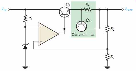
FIG. 8 -- Series regulator with constant-current limiting.
The load current through R4 produces a voltage from base to emitter of Q2. When IL reaches a predetermined maximum value, the voltage drop across R4 is sufficient to forward-bias the base-emitter junction of Q2, thus causing it to conduct. Enough op-amp output current is diverted through Q2 to reduce the Q1 base current, so that IL is limited to its maximum value, IL(max). Since the base-to-emitter voltage of Q2 cannot exceed approximately 0.7 V, the voltage across R4 is held to this value, and the load current is limited to:
IL(max) = 0.7V/R4 [ EQN. 6 ]
Regulator with Fold-Back Current Limiting
In the previous current-limiting technique, the current is restricted to a maximum constant value. Fold-back current limiting is a method used particularly in high-current regulators whereby the output current under overload conditions drops to a value well below the peak load current capability to prevent excessive power dissipation.
The basic concept of fold-back current limiting is as follows, with reference to FIG. 10. The circuit in the green-shaded area is similar to the constant current-limiting arrangement in FIG. 8, with the exception of resistors R5 and R6. The voltage drop developed across R4 by the load current must not only overcome the base-emitter voltage required to turn on Q2 but it must also overcome the voltage across R5. That is, the voltage across R4 must be:
VR4 = VR5 + VBE
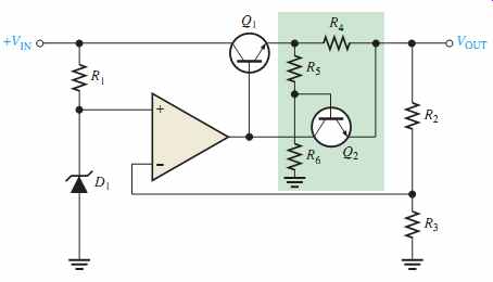
FIG. 10 Series regulator with fold-back current limiting.
In an overload or short-circuit condition, the load current increases to a value, IL(max), that is sufficient to cause Q2 to conduct. At this point the current can increase no further.
The decrease in output voltage results in a proportional decrease in the voltage across R5 thus, less current through R4 is required to maintain the forward-biased condition of Q1. So, as decreases, decreases, as shown in the graph of FIG. 11.
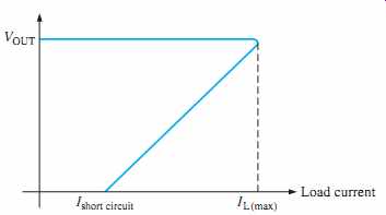
FIG. 11: Fold-back current limiting (output voltage versus load current).
The advantage of this technique is that the regulator is allowed to operate with peak load current up to IL(max); but when the output becomes shorted, the current drops to a lower value to prevent overheating of the device.
SECTION 2 CHECKUP
1. What are the basic components in a series regulator?
2. A certain series regulator has an output voltage of 8 V. If the op-amp's closed loop gain is 4, what is the value of the reference voltage?
3. BASIC LINEAR SHUNT REGULATORS
The second basic type of linear voltage regulator is the shunt regulator. As you have learned, the control element in the series regulator is the series-pass transistor.
In the shunt regulator, the control element is a transistor in parallel (shunt) with the load.
After completing this section, you should be able to
-- Describe and analyze the operation of linear shunt regulators: - Determine the maximum load current; - Compare series and shunt regulators
A simple representation of a shunt type of linear regulator is shown in FIG. 12(a), and the basic components are shown in the block diagram in part (b).
In the basic shunt regulator, the control element is a transistor, Q1, in parallel with the load, as shown in FIG. 13. A resistor, R1, is in series with the load. The operation of the circuit is similar to that of the series regulator, except that regulation is achieved by controlling the current through the parallel transistor Q1. When the output voltage tries to decrease due to a change in input voltage or load current caused by a change in load resistance, as shown in FIG. 14(a), the attempted decrease is sensed by R3 and R4 and applied to the op-amp's noninverting input. The resulting difference voltage reduces the op-amp's output driving less, thus reducing its collector current (shunt current) and increasing the collector voltage. Thus, the original decrease in voltage is compensated for by this increase, keeping the output nearly constant.
The opposite action occurs when the output tries to increase, as indicated in FIG. 14(b). With IL and VOUT constant, a change in the input voltage produces a change in shunt current (IS) as follows (Δ means "a change in"):
[Δ IS = Δ VIN/R1]

FIG. 12 Simple shunt regulator and block diagram.
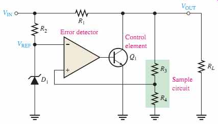
FIG. 13 Basic op-amp shunt regulator with load resistor.
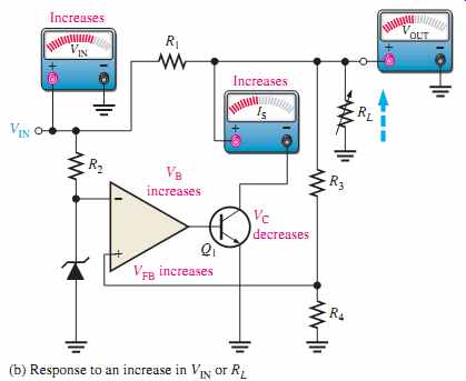

FIG. 14 Sequence of responses when VOUT tries to decrease as a result
of a decrease in RL or VIN (opposite responses for an attempted increase).
With a constant VIN and VOUT , a change in load current causes an opposite change in shunt current. If IL increases, IS decreases, and vice versa.
[Δ IS =-Δ IL]
The shunt regulator is less efficient than the series type but offers inherent short-circuit protection. If the output is shorted (VOUT = 0) the load current is limited by the series resistor R1 to a maximum value as follows (IS = 0).
SECTION 3 CHECKUP
1. How does the control element in a shunt regulator differ from that in a series regulator?
2. What is one advantage of a shunt regulator over a series type? What is a disadvantage?
---
4. BASIC SWITCHING REGULATORS
The two types of linear regulators, series and shunt, have control elements (transistors) that are conducting all the time, with the amount of conduction varied as demanded by changes in the output voltage or current. The switching regulator is different because the control element operates as a switch.
After completing this section, you should be able to:
-- Discuss the principles of switching regulators
-- Describe the step-down configuration of a switching regulator
-- Determine the output voltage of the step-down configuration
-- Describe the step-up configuration of a switching regulator
-- Describe the voltage-inverter configuration
A much greater efficiency can be realized with a switching type of voltage regulator than with the linear types because the transistor switches on and off and dissipates power only when it is on. In a linear regulator, the transistor is always on and constantly dissipates power because the transistor looks like a variable resistor. This causes heat to be generated and wastes power. In a switching regulator, the transistor operates only on the ends of the load line except during the very short switching time. As a result, efficiencies can be greater than 90%. Switching regulators are particularly useful where efficiency is important, such as for computers. An efficient converter avoids excessive heat, which can destroy electronic components.
Switching regulators are designed for various power levels. They range in power levels from less than one watt for some battery-operated portable equipment to hundreds and thou sands of watts in major applications. The requirements for the application determine the particular design, but all switching regulators require feedback to control the on-off time for the switch. Three basic configurations of switching regulators are step-down, step-up, and inverting. In some cases, such as a laptop computer, all three types may be employed for various parts of the system; for example, the display typically will use an inverting type, the microprocessor would use a step-down type, and the disk drive may use a step-up type.
Step-Down Configuration
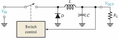
FIG. 16 Simplified step-down regulator.
In the step-down configuration (also called a buck converter), the output voltage is always less than the input voltage. The basic idea for a step-down type is shown in the simplified circuit shown in FIG. 16. The basic control element is a high-speed switch, which opens and closes rapidly from a control circuit that senses the output, and it adjusts the on time and the off-time to keep the desired output. When the switch is closed, the diode is off and the magnetic field of the inductor builds, storing energy. When the switch opens, the magnetic field collapses, keeping nearly constant current in the load. A path for the load current is provided through the forward-biased diode (as long as the load resistance is not too large). The capacitor smoothes the dc to a nearly constant level.
Let's look at the circuit, including the switching device, in more detail. The switch turns on and off the input voltage at a rapid rate and with a duty cycle that is based on the regulator's load requirement. FIG. 17 shows a basic step-down switching regulator using a D-MOSFET switching transistor. MOSFET transistors can switch faster than BJTs and have been improved in recent years, so they have become the preferred type of switching device, provided that the off-state voltage is not too high. As in most electronic devices, there are trade-offs for designers in choosing a switching device.
Differences in break-down voltage, on-state resistance, and switching time must all be considered for a given design. In addition to transistor switches, you may see thyristors used occasionally.
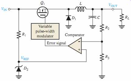
FIG. 17 A basic step-down switching regulator.
The pulsed current from the transistor switch is smoothed by an LC filter. The inductor tries to keep current constant, and the capacitor tends to keep voltage constant. Ideally, these components do not dissipate power, but in practice some loss is encountered due to various factors. To avoid requiring large (and expensive) inductors and capacitors, the switching frequency is selected to be much higher than the utility frequency; 20 kHz is common. The drawback to higher frequencies is electrical noise. Switching power supplies can radiate harmonic frequency noise to nearby circuits, so they need to be well shielded and frequently require EMI (electromagnetic interference) filters. Since the switching de vice spends most of its time either in cutoff or saturation, the power lost in the control element is usually relatively small (although instantaneous power dissipated in the switching device can be large).
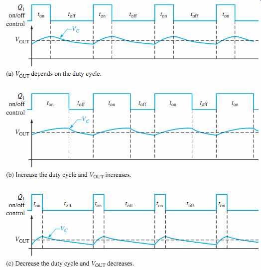
FIG. 18 Switching regulator waveforms. The VC waveform is shown for no
inductive filtering to illustrate the charge and discharge action (ripple).
L and C smooth VC to a nearly constant level, as indicated by the dashed
line for VOUT.
The on and off intervals of Q1 are shown in the waveform of FIG. 18(a). For an n-channel D-MOSFET, the control voltage swings between a negative value (off) to a positive value (on). The capacitor charges during the on-time (ton) and discharges during the off-time (toff). When the on-time is increased relative to the off-time, the capacitor charges more, thus increasing the output voltage, as indicated in FIG. 18(b). When the on-time is decreased relative to the off-time, the capacitor discharges more, thus decreasing the out put voltage, as in FIG. 18(c). The inductor further smoothes the fluctuations of the output voltage caused by the charging and discharging action.
Ideally, the output voltage is expressed as:
T is the period of the on-off cycle of and is related to the frequency by T = 1/f Q1. The period is the sum of the on-time and the off-time.
T = ton + toff
As you know ton/T the ratio is called the duty cycle.
The regulating action is as follows and is illustrated in FIG. 19. When VOUT tries to decrease, the on-time Q1 of is increased, causing an additional charge on C to offset the attempted decrease. When VOUT tries to increase Q1, the on-time of is decreased, causing the capacitor to discharge enough to offset the attempted increase.
Step-Up Configuration
A basic step-up type of switching regulator (sometimes called a boost converter) is shown in FIG. 20, where transistor Q1 operates as a switch to ground.
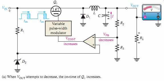
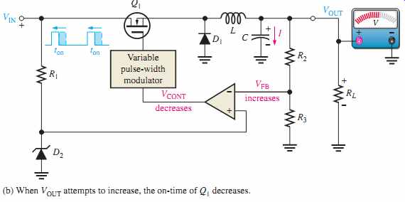
FIG. 19 Basic regulating action of a step down switching regulator.
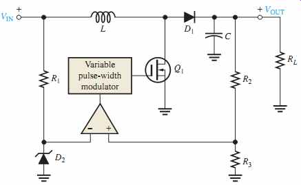
FIG. 20 Basic step-up switching regulator.
The switching action is illustrated in Figures 21 and 22. When Q1 turns on, a voltage equal to approximately VIN is induced across the inductor with a polarity as indicated in FIG. 21. During the on-time (ton) of Q1 the inductor voltage, VL, decreases from its initial maximum and diode D1 is reverse-biased. The longer Q1 is on, the smaller VL becomes. During the on-time, the capacitor only discharges an extremely small amount through the load.
When Q1 turns off, as indicated in FIG. 22, the inductor voltage suddenly reverses polarity and adds to VIN forward-biasing diode D1 and allowing the capacitor to charge.
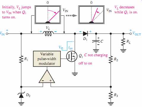
FIG. 21 Basic action of a step-up regulator when Q1 is on.
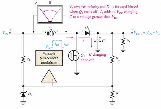
FIG. 22 Basic switching action of a step-up regulator when Q1 turns off.
The output voltage is equal to the capacitor voltage and can be larger than VIN because the capacitor is charged to VIN plus the voltage induced across the inductor during the off-time of Q1. The output voltage is dependent on both the inductor's magnetic field action (determined by ton) and the charging of the capacitor (determined by toff).
Voltage regulation is achieved by the variation of the on-time of Q1 (within certain limits) as related to changes in VOUT due to changing load or input voltage. If VOUT tries to increase, the on-time of Q1 will decrease, resulting in a decrease in the amount that C will charge. If VOUT tries to decrease, the on-time of Q1 will increase, resulting in an increase in the amount that C will charge. This regulating action maintains VOUT at an essentially constant level.
Voltage-Inverter Configuration
A third type of switching regulator produces an output voltage that is opposite in polarity to the input. A basic diagram is shown in FIG. 23. This is sometimes called a buck boost converter.
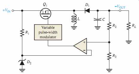
FIG. 23 Basic inverting switching regulator.
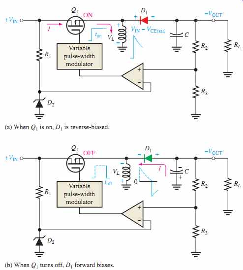
FIG. 24 Basic inverting action of an inverting switching regulator.
When Q1 turns on, the inductor voltage jumps to approximately VIN - VCE(sat) and the magnetic field rapidly expands, as shown in FIG. 24(a). While Q1 is on, the diode is reverse-biased and the inductor voltage decreases from its initial maximum. When Q1 turns off, the magnetic field collapses and the inductor's polarity reverses, as shown in FIG. 24(b). This forward-biases the diode, charges C, and produces a negative output voltage, as indicated. The repetitive on-off action of Q1 produces a repetitive charging and discharging that is smoothed by the LC filter action.
As with the step-up regulator, the less time is on, the greater the output voltage is, and vice versa. This regulating action is illustrated in FIG. 25.
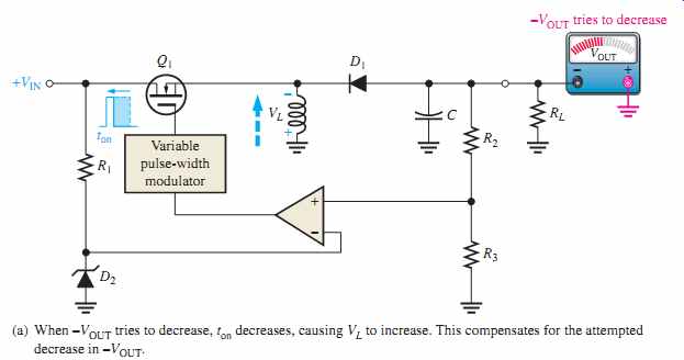
FIG. 25 Basic regulating action of an inverting switching regulator.
SECTION 4 CHECKUP
1. What are three types of switching regulators?
2. What is the primary advantage of switching regulators over linear regulators?
3. How are changes in output voltage compensated for in the switching regulator?


