AMAZON multi-meters discounts AMAZON oscilloscope discounts
5. RELAXATION OSCILLATORS
The second major category of oscillators is the relaxation oscillator. Relaxation oscillators use an RC timing circuit and a device that changes states to generate a periodic waveform. In this section, you will learn about several circuits that are used to pro duce nonsinusoidal waveforms.
After completing this section, you should be able to:
-- Describe and analyze the operation of relaxation oscillators
-- Describe the operation of a triangular-wave oscillator
-- Discuss a practical triangular-wave oscillator
-- Define function generator
-- Determine the UTP, LTP, and frequency of oscillation
-- Describe a sawtooth voltage-controlled oscillator (VCO)
-- Explain the purpose of the PUT in this circuit
-- Determine the frequency of oscillation
-- Describe a square-wave oscillator
A Triangular-Wave Oscillator
The op-amp integrator covered in Section 13 can be used as the basis for a triangular-wave oscillator. The basic idea is illustrated in FIG. 27(a) where a dual-polarity, switched input is used. We use the switch only to introduce the concept; it is not a practical way to implement this circuit. When the switch is in position 1, the negative voltage is applied, and the output is a positive-going ramp. When the switch is thrown into position 2, a negative-going ramp is produced. If the switch is thrown back and forth at fixed intervals, the output is a triangular wave consisting of alternating positive-going and negative-going ramps, as shown in FIG. 27(b).

FIG. 27 Basic triangular-wave oscillator. (b) Output voltage as the switch
is thrown back and forth at regular intervals
A Practical Triangular-Wave Oscillator
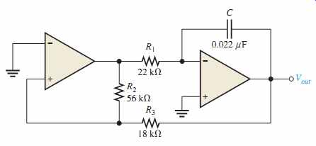
One practical implementation of a triangular wave oscillator utilizes an op-amp comparator with hysteresis to perform the switching function, as shown in FIG. 28. The operation is as follows. To begin, assume that the output voltage of the comparator is at its maximum negative level. This output is connected to the inverting input of the integrator through R1, producing a positive-going ramp on the output of the integrator. When the ramp voltage reaches the upper trigger point (UTP), the comparator switches to its maximum positive level. This positive level causes the integrator ramp to change to a negative-going direction. The ramp continues in this direction until the lower trigger point (LTP) of the comparator is reached. At this point, the comparator output switches back to the maximum negative level and the cycle repeats. This action is illustrated in FIG. 29.
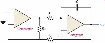
FIG. 28 A triangular-wave oscillator using two op-amps.
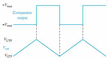
FIG. 29 Waveforms for the circuit in FIG. 28.
Since the comparator produces a square-wave output, the circuit in FIG. 28 can be used as both a triangular-wave oscillator and a square-wave oscillator. Devices of this type are commonly known as function generators because they produce more than one output function. The output amplitude of the square wave is set by the output swing of the comparator, and the resistors and set the amplitude of the triangular output by establishing the UTP and LTP voltages according to the following formulas:
---p826
where the comparator output levels, and are equal. The frequency of both waveforms depends on the time constant as well as the amplitude-setting resistors, and By varying the frequency of oscillation can be adjusted without changing the output amplitude.
A Sawtooth Voltage-Controlled Oscillator (VCO)
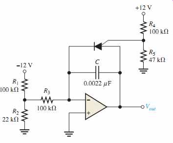
The voltage-controlled oscillator (VCO) is a relaxation oscillator whose frequency can be changed by a variable dc control voltage. VCOs can be either sinusoidal or nonsinusoidal. One way to build a sawtooth VCO is with an op-amp integrator that uses a switching device (PUT) in parallel with the feedback capacitor to terminate each ramp at a prescribed level and effectively "reset" the circuit. FIG. 31(a) shows the implementation.
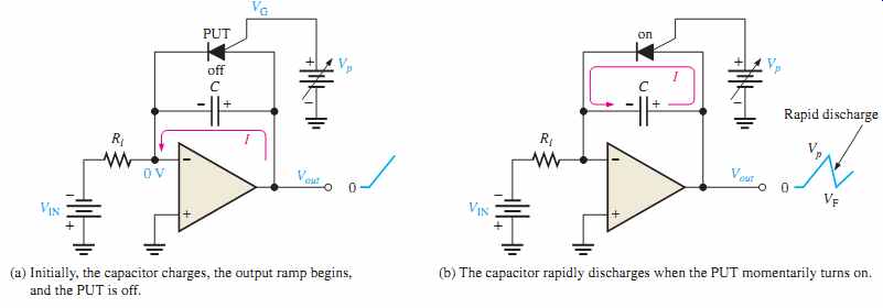
FIG. 31 Sawtooth VCO operation. (a) Initially, the capacitor charges,
the output ramp begins, and the PUT is off. (b) The capacitor rapidly discharges
when the PUT momentarily turns on.
As you learned in Section 11, the PUT is a programmable unijunction transistor with an anode, a cathode, and a gate terminal. The gate is always biased positively with respect to the cathode. When the anode voltage exceeds the gate voltage by approximately 0.7 V, the PUT turns on and acts as a forward-biased diode. When the anode voltage falls below this level, the PUT turns off. Also, the current must be above the holding value to maintain conduction.
The operation of the sawtooth VCO begins when the negative dc input voltage, produces a positive-going ramp on the output. During the time that the ramp is increasing, the circuit acts as a regular integrator. The PUT triggers on when the output ramp (at the anode) exceeds the gate voltage by 0.7 V. The gate is set to the approximate desired saw tooth peak voltage. When the PUT turns on, the capacitor rapidly discharges, as shown in FIG. 31(b). The capacitor does not discharge completely to zero because of the PUT's forward voltage, . Discharge continues until the PUT current falls below the holding value. At this point, the PUT turns off and the capacitor begins to charge again, thus generating a new output ramp. The cycle continually repeats, and the resulting output is a repetitive sawtooth waveform, as shown. The sawtooth amplitude and period can be adjusted by varying the PUT gate voltage.
The frequency of oscillation is determined by the time constant of the integrator and the peak voltage set by the PUT. Recall that the charging rate of a capacitor is
The time it takes a capacitor to charge from to is the period, T, of the sawtooth waveform (neglecting the rapid discharge time).
---p828
From f = 1>T,
EQN. 11
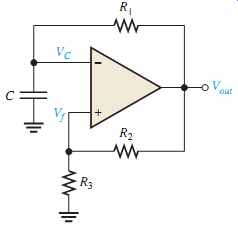
FIG. 34 A square-wave relaxation oscillator.
A Square-Wave Oscillator
The basic square-wave oscillator shown in FIG. 34 is a type of relaxation oscillator because its operation is based on the charging and discharging of a capacitor. Notice that the op-amp's inverting input is the capacitor voltage and the noninverting input is a portion of the output fed back through resistors R2 and R3 and to provide hysteresis. When the circuit is first turned on, the capacitor is uncharged, and thus the inverting input is at 0 V.
This makes the output a positive maximum, and the capacitor begins to charge toward Vout through R1. When the capacitor voltage reaches a value equal to the feedback voltage on the noninverting input, the op-amp switches to the maximum negative state. At this point, the capacitor begins to discharge from +Vf toward -Vf. When the capacitor voltage reaches the op-amp switches back to the maximum positive state. This action continues to repeat, as shown in FIG. 35, and a square-wave output voltage is obtained.
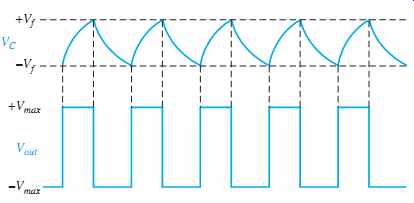
FIG. 35 Waveforms for the square-wave relaxation oscillator.
SECTION 5 CHECKUP
1. What is a VCO, and basically, what does it do?
2. Upon what principle does a relaxation oscillator operate?
6. THE 555 TIMER AS AN OSCILLATOR
The 555 timer is a versatile integrated circuit with many applications. In this section, you will see how the 555 is configured as an astable or free-running multivibrator, which is essentially a square-wave oscillator. The use of the 555 timer as a voltage controlled oscillator (VCO) is also discussed.
After completing this section, you should be able to:
-- Discuss and analyze the 555 timer and use it in oscillator applications
-- Describe the astable operation of a 555 timer
-- Determine the frequency of oscillation ? Determine the duty cycle
-- Discuss the 555 timer as a voltage-controlled oscillator
-- Describe the connections
The 555 timer consists basically of two comparators, a flip-flop, a discharge transistor, and a resistive voltage divider, as shown in FIG. 36. The flip-flop (bistable multivibrator) is a digital device that may be unfamiliar to you at this point unless you already have taken a digital fundamentals course. Briefly, it is a two-state device whose output can be at either a high voltage level (set, S) or a low voltage level (reset, R). The state of the output can be changed with proper input signals.
The resistive voltage divider is used to set the voltage comparator levels. All three resistors are of equal value; therefore, the upper comparator has a reference of 2/3VCC, and the lower comparator has a reference of 1/3VCC. The comparators' outputs control the state of the flip-flop. When the trigger voltage goes below 1/3VCC, the flip-flop sets and the output jumps to its high level. The threshold input is normally connected to an external RC timing circuit. When the external capacitor voltage exceeds 2/3VCC, the upper comparator resets the flip-flop, which in turn switches the output back to its low level.
When the device output is low, the discharge transistor is turned on and provides a path for rapid discharge of the external timing capacitor. This basic operation allows the timer to be configured with external components as an oscillator, a one-shot, or a time delay element.
(Qd)
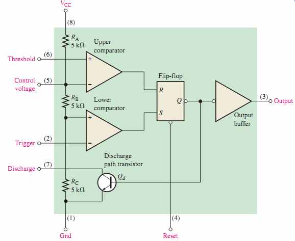
FIG. 36 Internal diagram of a 555 integrated circuit timer. (IC pin numbers
are in parentheses.)
Astable Operation
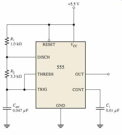
A 555 timer connected to operate in the astable mode as a free-running relaxation oscillator (astable multivibrator) is shown in FIG. 37. Notice that the threshold input (THRESH) is now connected to the trigger input (TRIG). The external components R1, R2, and Cext form the timing circuit that sets the frequency of oscillation. The capacitor 0.01 uF connected to the control (CONT) input is strictly for decoupling and has no effect on the operation.
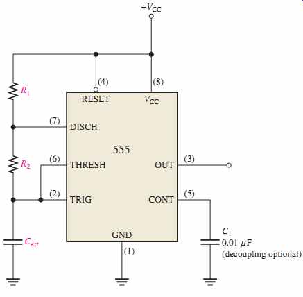
FIG. 37 The 555 timer connected as an astable multivibrator.
Initially, when the power is turned on, the capacitor is uncharged and thus the trigger voltage (pin 2) is at 0 V. This causes the output of the lower comparator to be high and the output of the upper comparator to be low, forcing the output of the flip-flop, and thus the base of low and keeping the transistor off. Now, Cext begins charging through R2 and as indicated in FIG. 38. When the capacitor voltage reaches 1/3VCC, the lower comparator switches to its low output state, and when the capacitor voltage reaches 2/3VCC, the upper comparator switches to its high output state. This resets the flip-flop, causes the base Qd of to go high, and turns on the transistor. This sequence creates a discharge path for the capacitor through and the transistor, as indicated. The capacitor now begins to discharge, causing the upper comparator to go low. At the point where the capacitor discharges down to 1/3VCC, the lower comparator switches high, setting the flip-flop, which makes the base of Qd low and turns off the transistor. Another charging cycle begins, and the entire process repeats. The result is a rectangular wave output whose duty cycle depends on the values of R1 and R2.
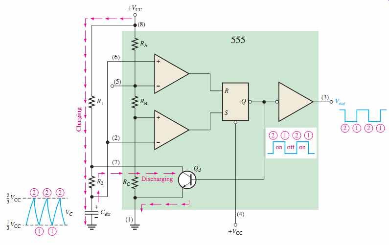
FIG. 38 Operation of the 555 timer in the astable mode.
The frequency of oscillation is given by EQN. 12, or it can be found using the graph in FIG. 39.
EQN. 12
By selecting and the duty cycle of the output can be adjusted. Since charges through and discharges only through duty cycles approaching a minimum of 50 percent can be achieved if so that the charging and discharging times are approximately equal.
1/3VCC to 2/3VCC. It is expressed as
Cext (tH) R2 77 R1 R2, R1 + R2 Cext R2, R1
A formula to calculate the duty cycle is developed as follows. The time that the output is high is how long it takes to charge from
tH = 0.694(R1 + R2)Cext

FIG. 39 Frequency of oscillation (free-running frequency) of a 555 timer
in the astable mode as a function of Cext and R1 _ 2R2. The sloped lines
are values of R1 _ 2R2.
The time that the output is low is how long it takes to discharge from 2/3VCC to 1/3VCC. It is expressed as
The period, T, of the output waveform is the sum of and
The following formula for T is the reciprocal of f in EQN. 12.
Finally, the percent duty cycle is
Duty cycle = a tH T b100% = a tH tH + tL b100%
T = tH + tL = 0.694(R1 + 2R2)Cext tL. tH tL = 0.694R2Cext Cext (tL)
To achieve duty cycles of less than 50 percent, the circuit in FIG. 37 can be modified so that charges through only and discharges through This is achieved with a diode, placed as shown in FIG. 40. The duty cycle can be made less than 50
D1,
R2. R1 Cext
Duty cycle _ a R1 _ R2 R1 _ 2R2 b100%
FIG. 40 The addition of diode D1 allows the duty cycle of the output to be adjusted to less than 50 percent by making R1 < R2.
percent by making less than
Under this condition, the formulas for the frequency and percent duty cycle are (assuming an ideal diode)
R2. R1
Operation as a Voltage-Controlled Oscillator (VCO)
A 555 timer can be set up to operate as a VCO by using the same external connections as for astable operation, with the exception that a variable control voltage is applied to the CONT input (pin 5), as indicated in FIG. 42.
As shown in FIG. 43, the control voltage changes the threshold values of 1/3VCC and 2/3VCC for the internal comparators. With the control voltage, the upper value is and the lower value is 1/2VCONT, as you can see by examining the internal diagram of the 555 timer. When the control voltage is varied, the output frequency also varies. An VCONT (VCONT) increase in increases the charging and discharging time of the external capacitor and causes the frequency to decrease. A decrease in decreases the charging and discharging time of the capacitor and causes the frequency to increase.
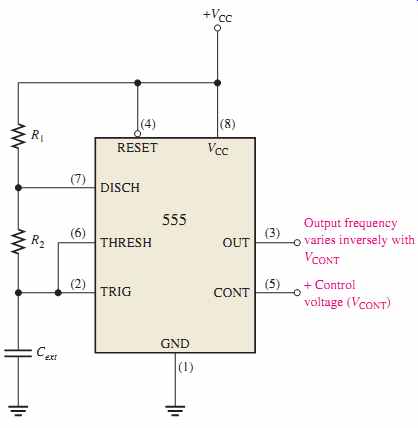
FIG. 42 The 555 timer connected as a voltage-controlled oscillator (VCO).
Note the variable control voltage input on pin 5.

FIG. 43 The VCO output frequency varies inversely with VCONT because the
charging and discharging time of Cext is directly dependent on the control
voltage.
An interesting application of the VCO is in phase-locked loops, which are used in various types of communication receivers to track variations in the frequency of incoming signals.
VCONT VCONT
SECTION 6 CHECKUP
1. Name the five basic elements in a 555 timer IC.
2. When the 555 timer is configured as an astable multivibrator, how is the duty cycle determined?
===============
Application Activity: ASK Test Generator
The RFID reader board that was developed in the Section 15 Application Activity re quires an ASK modulated source to test it. Recall that the RFID tag transmits a 125 kHz ASK (amplitude shift keyed) signal modulated with coded information represented by a digital waveform. The basic block diagram is shown in FIG. 44.
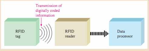
FIG. 44 Basic block diagram of an RFID system.
The ASK Test Generator
The purpose of this application is to develop a signal source for testing the RFID reader circuit board. The source must produce a 125 kHz signal that is modulated with a 10 kHz pulse signal to simulate the RFID tag. An oscillator is used to generate the 125 kHz carrier signal, and a 555 timer produces the modulating pulse signal. The modulating device is an analog switch that allows the carrier signal to be turned on and off by the modulating pulse signal. A basic block diagram is shown in FIG. 45.
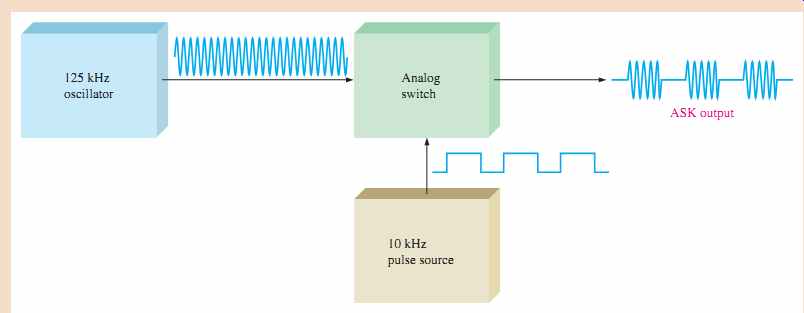
FIG. 45 Basic block diagram of the ASK test generator.
Simulation The first step is to design the 125 kHz oscillator circuit. The type of oscillator chosen for this application is the Colpitts oscillator. The simulated circuit is shown in FIG. 46(a), and the output waveform is shown in part (b).
1. Calculate the gain of the Colpitts oscillator in FIG. 46.
2. Calculate the frequency of the Colpitts oscillator and compare to the frequency measured in the simulation.
In the second step, the 10 kHz pulse oscillator is designed using a 555 timer. The simulated circuit and output waveform are shown in FIG. 47.
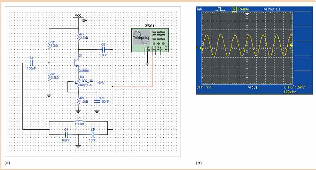
FIG. 46 Colpitts oscillator for generating the 125 kHz carrier signal.
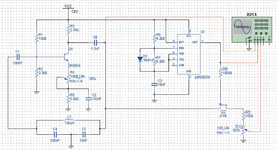
FIG. 47 555 timer configured for generating a 10 kHz square wave.
3. Calculate the frequency of the pulse oscillator in FIG. 47 and compare to the measured frequency in the simulation.
4. Describe a possible reason for the difference in the calculated and the simulated value of frequency.
The third step in the simulation of the ASK test generator is to combine the Colpitts oscillator with the 555 timer and add an analog switch. For the purpose of switching the carrier signal on and off, a p-channel JFET is used. When the timer output is low, the JFET turns on and passes the carrier signal to the ASK output. When the timer output is high, the JFET turns off and blocks the signal from the output. The complete circuit is shown in FIG. 48, and the resulting waveforms are shown in FIG. 49.
5. What is the purpose of Q2 in the ASK test generator circuit? Finally, a simulation is run with the ASK test generator driving the RFID reader. This is shown in FIG. 50.
6. Identify each waveform in FIG. 50.

FIG. 48 The complete ASK test generator.
Simulate the ASK test generator using your Multisim software. Observe the operation with the oscilloscope.
Prototyping and Testing
Now that the circuit has been simulated, the prototype circuit is constructed and tested.
After the circuit is successfully tested on a protoboard, it is ready to be finalized on a printed circuit board.
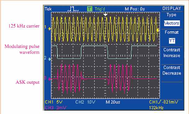
FIG. 49 Waveforms for the ASK test generator.
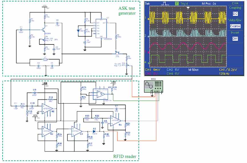
FIG. 50 Simulation of the ASK test generator driving the RFID reader.
Lab Experiment
To build and test a circuit similar to one used in the ASK test generator, go to Experiment 16-A in your lab manual (Laboratory Exercises for Electronic Devices by David Buchla and Steven Wetterling).
Circuit Board
The ASK test generator is implemented on a printed circuit board as shown in FIG. 51 and will be housed in a unit for use in testing RFID readers on the assembly line.
The dark gray lines represent backside connections.
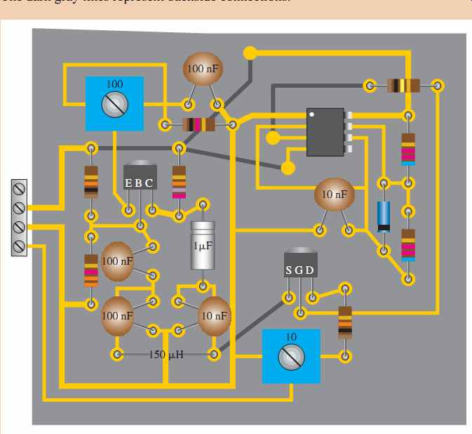
FIG. 51 ASK test generator board.
7. Check the printed circuit board and verify that it agrees with the simulation schematic in FIG. 48.
8. Label each input and output pin according to function.
============================
Programmable Analog Technology
Oscillators with various types of outputs can be programmed into an FPAA or a dpASP. These are described as follows.
Sine-Wave Oscillator
Oscillators can be implemented in programmable analog arrays using software. A sine-wave oscillator is shown in FIG. 52 using AnadigmDesigner2.
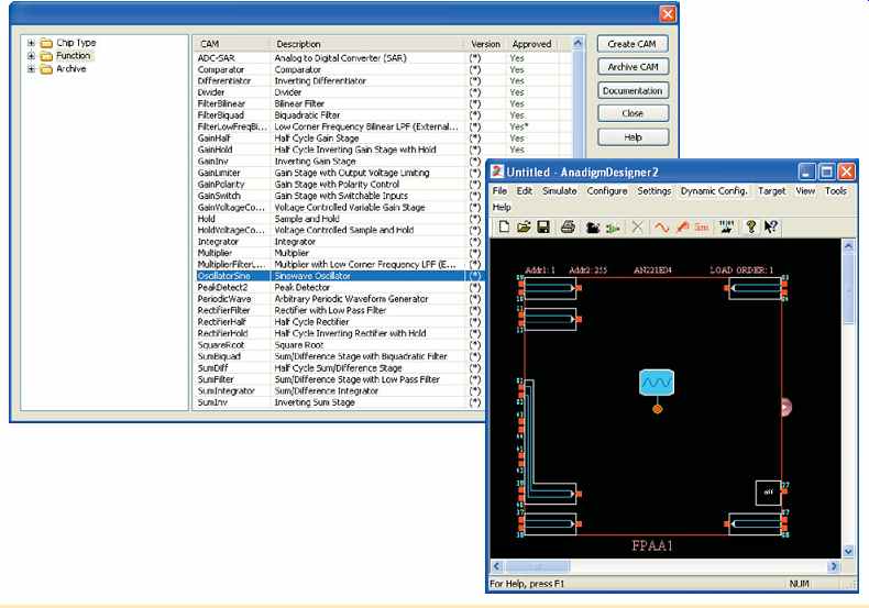
FIG. 52 Selection and placement of the sine-wave oscillator CAM.
The frequency and peak amplitude of the oscillator can be programmed, and the oscillator CAM can be connected to an output as shown in FIG. 53(a). Running the simulation produces the results shown in part (b).
Square-Wave Oscillator
A square-wave oscillator can be programmed using the sine-wave oscillator CAM and the comparator CAM, as illustrated in FIG. 54. The frequency of the square wave can be changed by re programming the frequency of the sine-wave oscillator.
Variable Duty Cycle Pulse Oscillator
By adding a variable reference to the comparator CAM and by changing its value, the duty cycle as well as the frequency of the pulse waveform can be varied, as shown in FIG. 55.
Triangular-Wave Oscillator
One way to program a triangular-wave oscillator is shown in FIG. 56. A sine-wave oscillator is used to drive an inverting gain stage into nonlinear operation. This is followed by an integrator with a properly selected integration constant. A comparator could have been used instead of the over-driven gain stage except that Designer2 does not allow the output of a comparator to be connected to anything but a chip output.
Programming Exercises
1. How do you adjust the duty cycle of the variable duty cycle pulse oscillator?
2. To change the frequency of the triangular-wave oscillator, what parameters must be changed by programming?
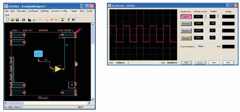
FIG. 54 A square-wave oscillator.

FIG. 53 Programming a chip as a sine-wave oscillator.
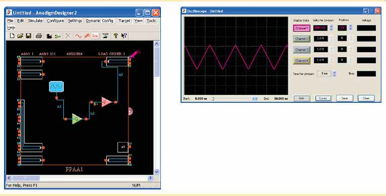
FIG. 56 A triangular-wave oscillator.
SUMMARY
SECTION 1
-- Sinusoidal feedback oscillators operate with positive feedback.
-- Relaxation oscillators use an RC timing circuit.
SECTION 2
-- The two conditions for positive feedback are the phase shift around the feedback loop must be and the voltage gain around the feedback loop must equal 1.
-- For initial start-up, the voltage gain around the feedback loop must be greater than 1.
SECTION 3
-- Sinusoidal RC oscillators include the Wien-bridge, phase-shift, and twin-T.
SECTION 4
-- Sinusoidal LC oscillators include the Colpitts, Clapp, Hartley, Armstrong, and crystal controlled.
-- The feedback signal in a Colpitts oscillator is derived from a capacitive voltage divider in the LC circuit.
-- The Clapp oscillator is a variation of the Colpitts with a capacitor added in series with the inductor.
-- The feedback signal in a Hartley oscillator is derived from an inductive voltage divider in the LC circuit.
-- The feedback signal in an Armstrong oscillator is derived by transformer coupling.
-- Crystal oscillators are the most stable type of feedback oscillator.
SECTION 5
A relaxation oscillator uses an RC timing circuit and a device that changes states to generate a periodic waveform.
-- The frequency in a voltage-controlled oscillator (VCO) can be varied with a dc control voltage.
SECTION 6
The 555 timer is an integrated circuit that can be used as an oscillator, in addition to many other applications.
0°
TERMS USED
Key terms and other bold terms in the Section are defined in the end-of-book glossary.
Astable -- Characterized by having no stable states.
Oscillator -- An electronic circuit that produces a periodic waveform on its output with only the dc supply voltage as an input.
Positive feedback -- The return of a portion of the output signal to the input such that it reinforces and sustains the output.
Voltage-controlled oscillator (VCO) -- A type of relaxation oscillator whose frequency can be varied by a dc control voltage.
FORMULAS
Wien-bridge positive feedback attenuation Wien-bridge resonant frequency Phase-shift feedback attenuation Phase-shift oscillator frequency Colpitts, Clapp, and Hartley approximate resonant frequency Colpitts amplifier gain
Colpitts resonant frequency Hartley self-starting gain Armstrong resonant frequency Triangular-wave oscillator frequency Sawtooth VCO frequency 555 astable frequency 555 astable
TRUE/FALSE QUIZ
1. Two categories of oscillators are feedback and relaxation.
2. A feedback oscillator uses only negative feedback.
3. Positive feedback is never used in an oscillator.
4. The net phase shift around the oscillator feedback loop must be zero.
5. The voltage gain around the closed feedback loop must be greater than 1 to sustain oscillations.
6. For start-up, the loop gain must be greater than 1.
7. A Wien-bridge oscillator uses an RC circuit in the positive feedback loop.
8. The phase-shift oscillator utilizes RC circuits.
9. The twin-T oscillator contains an LC feedback circuit.
10. Colpitts, Clapp, Hartley, and Armstrong are examples of LC oscillators.
11. The crystal oscillator is based on the photoelectric effect.
12. A relaxation oscillator uses no positive feedback.
13. Most relaxation oscillators produce sinusoidal outputs.
14. VCO stands for variable-capacitance oscillator.
15. The 555 timer can be used as an oscillator.
CIRCUIT-ACTION QUIZ
1. If and are increased to in FIG. 12, the frequency of oscillation will (a) increase (b) decrease (c) not change
2. If the feedback potentiometer is adjusted to a higher value, the voltage gain in FIG. 12 will (a) increase (b) decrease (c) not change
3. In FIG. 14, if the is decreased, the feedback attenuation will (a) increase (b) decrease (c) not change
4. If the capacitors in FIG. 14 are increased to the frequency of oscillation will (a) increase (b) decrease (c) not change
5. In order to increase in FIG. 30, must (a) increase (b) decrease (c) not change
6. If the capacitor in FIG. 30 opens, the frequency of oscillation will (a) increase (b) decrease (c) not change
R3 VUTP
0.01 mF, Rf Rf 18 kOhm R2 R1
7. If the value of R1 in FIG. 32 is decreased, the peak value of the sawtooth output will (a) increase (b) decrease (c) not change
8. If the diode in FIG. 40 opens, the duty cycle will (a) increase (b) decrease (c) not change
SELF-TEST
SECTION 1
1. An oscillator differs from an amplifier because the oscillator (a) has more gain (b) requires no input signal (c) requires no dc supply (d) always has the same output SECTION 2
2. One condition for oscillation is (a) a phase shift around the feedback loop of 180° (b) a gain around the feedback loop of one-third (c) a phase shift around the feedback loop of 0° (d) a gain around the feedback loop of less than 1
3. A second condition for oscillation is (a) no gain around the feedback loop (b) a gain of 1 around the feedback loop (c) the attenuation of the feedback circuit must be one-third (d) the feedback circuit must be capacitive
4. In a certain oscillator, The attenuation of the feedback circuit must be (a) 1 (b) 0.01 (c) 10 (d) 0.02
5. For an oscillator to properly start, the gain around the feedback loop must initially be (a) 1 (b) less than 1 (c) greater than 1 (d) equal to B
SECTION 3
6. Wien-bridge oscillators are based on (a) positive feedback (b) negative feedback (c) the piezoelectric effect (d) high gain
7. In a Wien-bridge oscillator, if the resistances in the positive feedback circuit are decreased, the frequency (a) decreases (b) increases (c) remains the same
8. The Wien-bridge oscillator's positive feedback circuit is (a) an RL circuit (b) an LC circuit (c) a voltage divider (d) a lead-lag circuit
9. A phase-shift oscillator has (a) three RC circuits (b) three LC circuits (c) a T-type circuit (d) a -type circuit
SECTION 4
10. Colpitts, Clapp, and Hartley are names that refer to (a) types of RC oscillators (b) inventors of the transistor (c) types of LC oscillators (d) types of filters
11. The main feature of a crystal oscillator is (a) economy (b) reliability (c) stability (d) high frequency
SECTION 5
12. An oscillator whose frequency is changed by a variable dc voltage is known as (a) a crystal oscillator (b) a VCO (c) an Armstrong oscillator (d) a piezoelectric device
13. The operation of a relaxation oscillator is based on (a) the charging and discharging of a capacitor (b) a highly selective resonant circuit (c) a very stable supply voltage (d) low power consumption p Av = 50.
SECTION 6
14. Which one of the following is not an input or output of the 555 timer? (a) Threshold (b) Control voltage (c) Clock (d) Trigger (e) Discharge (f ) Reset
PROBLEMS
BASIC PROBLEMS
SECTION 1
The Oscillator
1. What type of input is required for an oscillator?
2. What are the basic components of an oscillator circuit?
SECTION 2
Feedback Oscillators
3. If the voltage gain of the amplifier portion of an oscillator is 75, what must be the attenuation of the feedback circuit to sustain the oscillation?
4. Generally describe the change required in the oscillator of Problem 3 in order for oscillation to begin when the power is initially turned on.
SECTION 3
Oscillators with RC Feedback Circuits
5. A certain lead-lag circuit has a resonant frequency of 3.5 kHz. What is the rms output voltage if an input signal with a frequency equal to and with an rms value of 2.2 V is applied to the input?
6. Calculate the resonant frequency of a lead-lag circuit with the following values: and
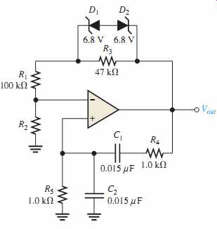
7. Determine the necessary value of in FIG. 57 so that the circuit will oscillate. Neglect the forward resistance of the zener diodes. (Hint: The total gain of the circuit must be 3 when the zener diodes are conducting.)
8. Explain the purpose of in FIG. 57.
R3 R2 C1 = C2 = 0.02 mF.
R1 = R2 = 6.2 kÆ, fr
9. For the Wien-bridge oscillator in FIG. 58, calculate the setting for assuming the internal drain-source resistance, of the JFET is when oscillations are stable.
10. Find the frequency of oscillation for the Wien-bridge oscillator in FIG. 58.
350 ohm r¿ ds, Rf,
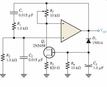
FIG. 58 Multisim file circuits are identified with a logo and are in the
Problems folder on the companion website.
Filenames correspond to figure numbers (e.g., F16-58).
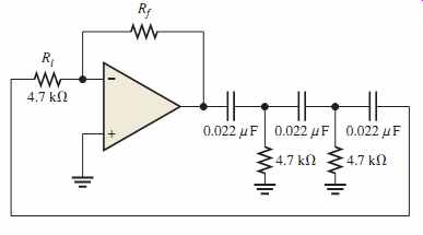
11. What value of is required in FIG. 59? What is fr? Rf
SECTION 4
Oscillators with LC Feedback Circuits
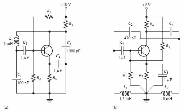
12. Calculate the frequency of oscillation for each circuit in FIG. 60 and identify the type of oscillator. Assume in each case. Q 7 10
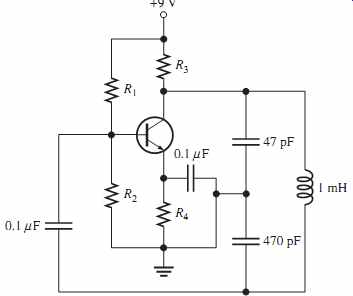
13. Determine what the gain of the amplifier stage must be in FIG. 61 in order to have sustained oscillation.
SECTION 5
Relaxation Oscillators
14. What type of signal does the circuit in FIG. 62 produce? Determine the frequency of the output.
15. Show how to change the frequency of oscillation in FIG. 62 to 10 kHz.
16. Determine the amplitude and frequency of the output voltage in FIG. 63. Use 1 V as the forward PUT voltage.
17. Modify the sawtooth generator in FIG. 63 so that its peak-to-peak output is 4 V.
18. A certain sawtooth generator has the following parameter values: VIN = 3V, R = 4.7 kOhm, Determine its peak-to-peak output voltage if the period is 10 ms. C = 0.001 mF.
SECTION 6
The 555 Timer as an Oscillator
19. What are the two comparator reference voltages in a 555 timer when 20. Determine the frequency of oscillation for the 555 astable oscillator in FIG. 64.
21. To what value must be changed in FIG. 64 to achieve a frequency of 25 kHz?
22. In an astable 555 configuration, the external resistor What must equal to produce a duty cycle of 75 percent?
R2 R1 = 3.3 kOhm.
Cext VCC = 10 V?

