AMAZON multi-meters discounts AMAZON oscilloscope discounts
SECTION OUTLINE
_1 The Oscillator
_2 Feedback Oscillators
_3 Oscillators with RC Feedback Circuits
_4 Oscillators with LC Feedback Circuits
_5 Relaxation Oscillators
_6 The 555 Timer as an Oscillator Application Activity Programmable Analog Technology
GOALS
-- Describe the operating principles of an oscillator
-- Discuss the principle on which feedback oscillators is based
-- Describe and analyze the operation of RC feedback oscillators
-- Describe and analyze the operation of LC feedback oscillators
-- Describe and analyze the operation of relaxation oscillators
-- Discuss and analyze the 555 timer and use it in oscillator applications
TERMS USED
-- Oscillator
-- Positive feedback
-- Voltage-controlled oscillator (VCO)
-- Astable
APPLICATION ACTIVITY PREVIEW
The application in this Section is a circuit that produces an ASK signal for testing the RFID reader developed in the last Section.
The ASK test generator uses an oscillator, a 555 timer, and a JFET analog switch to produce a 125 kHz carrier signal modulated at 10 kHz by a digital signal. The output amplitude is adjustable down to a low level to simulate the RFID tag signal.
INTRODUCTION
Oscillators are electronic circuits that generate an output signal without the necessity of an input signal. They are used as signal sources in all sorts of applications. Different types of oscillators produce various types of outputs including sine waves, square waves, triangular waves, and sawtooth waves.
In this Section, several types of basic oscillator circuits using both discrete transistors and op-amps as the gain element are introduced. Also, a popular integrated circuit, the 555 timer, is discussed in relation to its oscillator applications.
Sinusoidal oscillator operation is based on the principle of positive feedback, where a portion of the output signal is fed back to the input in a way that causes it to reinforce itself and thus sustain a continuous output signal. Oscillators are widely used in most communications systems as well as in digital systems, including computers, to generate required frequencies and timing signals. Also, oscillators are found in many types of test instruments like those used in the laboratory.
1. THE OSCILLATOR
An oscillator is a circuit that produces a periodic waveform on its output with only the dc supply voltage as an input. A repetitive input signal is not required except to synchronize oscillations in some applications. The output voltage can be either sinusoidal or nonsinusoidal, depending on the type of oscillator. Two major classifications for oscillators are feedback oscillators and relaxation oscillators.
After completing this section, you should be able to:
-- Describe the operating principles of an oscillator
-- Discuss feedback oscillators
-- List the basic elements of a feedback oscillator ? Show a test setup
-- Briefly describe a relaxation oscillator
-- State the difference between a feedback oscillator and a relaxation oscillator
Essentially, an oscillator converts electrical energy from the dc power supply to periodic waveforms. A basic oscillator is shown in FIG. 1.
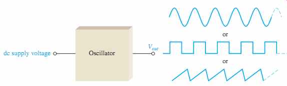
FIG. 1 The basic oscillator concept showing three common types of output
wave forms: sine wave, square wave, and sawtooth.
Feedback Oscillators
One type of oscillator is the feedback oscillator, which returns a fraction of the output signal to the input with no net phase shift, resulting in a reinforcement of the output signal. After oscillations are started, the loop gain is maintained at 1.0 to maintain oscillations. A feedback oscillator consists of an amplifier for gain (either a discrete transistor or an op-amp) and a positive feedback circuit that produces phase shift and provides attenuation, as shown in FIG. 2.
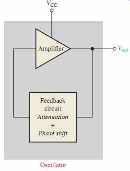
FIG. 2 Basic elements of a feedback oscillator.
Relaxation Oscillators
A second type of oscillator is the relaxation oscillator. Instead of feedback, a relaxation oscillator uses an RC timing circuit to generate a waveform that is generally a square wave or other nonsinusoidal waveform. Typically, a relaxation oscillator uses a Schmitt trigger or other device that changes states to alternately charge and discharge a capacitor through a resistor. Relaxation oscillators are discussed in SECTION 5.
1. What is an oscillator?
2. What type of feedback does a feedback oscillator require?
3. What is the purpose of the feedback circuit?
4. Name the two types of oscillators.
_2 FEEDBACK OSCILLATORS
Feedback oscillator operation is based on the principle of positive feedback. In this section, we will examine this concept and look at the general conditions required for oscillation to occur. Feedback oscillators are widely used to generate sinusoidal waveforms.
After completing this section, you should be able to:
-- Discuss the principle on which feedback oscillators is based
-- Explain positive feedback
-- Define oscillation
-- Describe the conditions for oscillation
-- Define closed loop gain
-- Discuss the conditions required for oscillator start-up
Positive Feedback
Positive feedback is characterized by the condition wherein a portion of the output voltage of an amplifier is fed back to the input with no net phase shift, resulting in a reinforcement of the output signal. This basic idea is illustrated in FIG. 3(a). As you can see, the in phase feedback voltage, Vf is amplified to produce the output voltage, which in turn produces the feedback voltage. That is, a loop is created in which the signal sustains itself and a continuous sinusoidal output is produced. This phenomenon is called oscillation. In some types of amplifiers, the feedback circuit shifts the phase and an inverting amplifier is required to provide another phase shift so that there is no net phase shift. This is illustrated in FIG. 3(b).
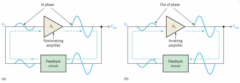
FIG. 3 Positive feedback produces oscillation.
Conditions for Oscillation
Two conditions, illustrated in FIG. 4, are required for a sustained state of oscillation:
1. The phase shift around the feedback loop must be effectively
2. The voltage gain, around the closed feedback loop (loop gain) must equal 1 (unity).
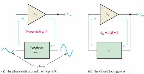
FIG. 4 General conditions to sustain oscillation.
The voltage gain around the closed feedback loop, is the product of the amplifier gain, and the attenuation, B, of the feedback circuit.
Acl = Av B
If a sinusoidal wave is the desired output, a loop gain greater than 1 will rapidly cause the output to saturate at both peaks of the waveform, producing unacceptable distortion. To avoid this, some form of gain control must be used to keep the loop gain at exactly 1 once oscillations have started. For example, if the attenuation of the feedback circuit is 0.01, the amplifier must have a gain of exactly 100 to overcome this attenuation and not create unacceptable distortion.
An amplifier gain of greater than 100 will cause the oscillator to limit both peaks of the waveform.
Start-Up Conditions
So far, you have seen what it takes for an oscillator to produce a continuous sinusoidal out put. Now let's examine the requirements for the oscillation to start when the dc supply voltage is first turned on. As you know, the unity-gain condition must be met for oscillation to be sustained. For oscillation to begin, the voltage gain around the positive feedback loop must be greater than 1 so that the amplitude of the output can build up to a desired level.
The gain must then decrease to 1 so that the output stays at the desired level and oscillation is sustained. Ways that certain amplifiers achieve this reduction in gain after start-up are discussed in later sections of this Section. The voltage gain conditions for both starting and sustaining oscillation are illustrated in FIG. 5.
A question that normally arises is this: If the oscillator is initially off and there is no out put voltage, how does a feedback signal originate to start the positive feedback buildup process? Initially, a small positive feedback voltage develops from thermally produced broad-band noise in the resistors or other components or from power supply turn-on transients. The feedback circuit permits only a voltage with a frequency equal to the selected oscillation frequency to appear in phase on the amplifier's input. This initial feedback voltage is amplified and continually reinforced, resulting in a buildup of the output voltage as previously discussed.
FIG. 5 When oscillation starts at t0, the condition Acl > 1 causes the sinusoidal output voltage amplitude to build up to a desired level. Then Acl decreases to 1 and maintains the desired amplitude.
SECTION 2 CHECKUP
1. What are the conditions required for a circuit to oscillate?
2. Define positive feedback.
3. What is the voltage gain condition for oscillator start-up?
_3 OSCILLATORS WITH RC FEEDBACK CIRCUITS
Three types of feedback oscillators that use RC circuits to produce sinusoidal outputs are the Wien-bridge oscillator, the phase-shift oscillator, and the twin-T oscillator.
Generally, RC feedback oscillators are used for frequencies up to about 1 MHz. The Wien-bridge is by far the most widely used type of RC feedback oscillator for this range of frequencies.
After completing this section, you should be able to
-- Describe and analyze the operation of RC feedback oscillators
-- Identify and describe the Wien-bridge oscillator
-- Discuss the response of a lead-lag circuit
-- Discuss the attenuation of the lead-lag circuit
-- Calculate the resonant frequency
-- Discuss the positive feedback conditions for oscillation
-- Describe the start-up conditions
-- Discuss a JFET stabilized Wien-bridge oscillator
-- Describe and analyze the phase-shift oscillator
-- Discuss the required value of feedback attenuation
-- Calculate the resonant frequency
-- Discuss the twin-T oscillator
The Wien-Bridge Oscillator
One type of sinusoidal feedback oscillator is the Wien-bridge oscillator. A fundamental part of the Wien-bridge oscillator is a lead-lag circuit like that shown in FIG. 6(a).R1 and C1 together form the lag portion of the circuit; and form the lead portion. The operation of this lead-lag circuit is as follows. At lower frequencies, the lead circuit dominates due to the high reactance of As the frequency increases, decreases, thus al lowing the output voltage to increase. At some specified frequency, the response of the lag circuit takes over, and the decreasing value of causes the output voltage to decrease.
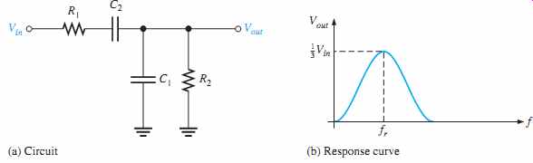
FIG. 6 A lead-lag circuit and its response curve.
The response curve for the lead-lag circuit shown in FIG. 6(b) indicates that the out put voltage peaks at a frequency called the resonant frequency, fr. At this point, the attenuation (Vout/Vin) of the circuit is 1/3 if R and X_c1 = X_c2 as stated by the following equation:

EQN. 1
The formula for the resonant frequency (also derived on the companion website) is:

EQN. 2
To summarize, the lead-lag circuit in the Wien-bridge oscillator has a resonant frequency fr, at which the phase shift through the circuit is and the attenuation is 1/3.
Below the lead circuit dominates and the output leads the input. Above fr, the lag circuit dominates and the output lags the input.
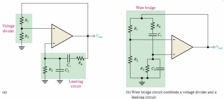
FIG. 7 The Wien-bridge oscillator schematic drawn in two different but
equivalent ways.
The Basic Circuit
The lead-lag circuit is used in the positive feedback loop of an op amp, as shown in FIG. 7(a). A voltage divider is used in the negative feedback loop.
The Wien-bridge oscillator circuit can be viewed as a noninverting amplifier configuration with the input signal fed back from the output through the lead-lag circuit. Recall that the voltage divider determines the closed-loop gain of the amplifier.
Acl = 1 / B = 1 / [R2>(R1 + R2)] = [R1 + R2] / R2
The circuit is redrawn in FIG. 7(b) to show that the op-amp is connected across the bridge circuit. One leg of the bridge is the lead-lag circuit, and the other is the voltage divider.
Positive Feedback Conditions for Oscillation
As you know, for the circuit to produce a sustained sinusoidal output (oscillate), the phase shift around the positive feedback loop must be 0° and the gain around the loop must equal unity (1). The 0° phase-shift condition is met when the frequency is fr because the phase shift through the lead-lag circuit is 0° and there is no inversion from the noninverting (+_) input of the op-amp to the output. This is shown in FIG. 8(a).
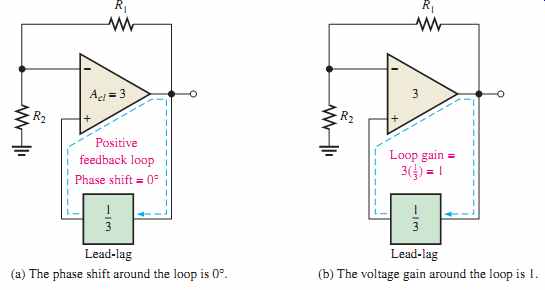
FIG. 8 Conditions for sustained oscillation. (b) The voltage gain around
the loop is 1. (a) The phase shift around the loop is 0°.
The unity-gain condition in the feedback loop is met when:
Acl = 3
This offsets the 1/3 attenuation of the lead-lag circuit, thus making the total gain around the positive feedback loop equal to 1, as depicted in FIG. 8(b). To achieve a closed-loop gain of 3,
R1 = 2R2
Then:
Acl = [R1 + R2]/ R2 = [2R2 + R2]/ R2 = 3R2/R2 = 3
---------
HISTORY NOTE
Max Wien (1866-1938) was a German physicist. He theoretically developed the concept of the Wien-bridge oscillator in 1891. At that time, Wien did not have a means of developing electronic gain, so a workable oscillator could not be achieved. Based on Wien's work, William Hewlett, co-founder of Hewlett-Packard, was successful in building a practical Wien-bridge oscillator in 1939.
---------
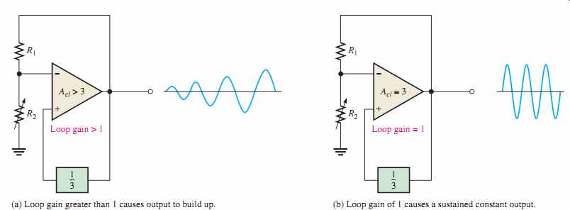
FIG. 9 Conditions for start-up and sustained oscillations. (a) Loop gain
greater than 1 causes output to build up. (b) Loop gain of 1 causes a sustained
constant output.
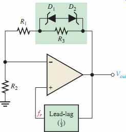
FIG. 10 Self-starting Wien-bridge oscillator using back-to-back zener
diodes.
Start-Up Conditions
Initially, the closed-loop gain of the amplifier itself must be more than 3 (Acl > 3) until the output signal builds up to a desired level. Ideally, the gain of the amplifier must then decrease to 3 so that the total gain around the loop is 1 and the output signal stays at the desired level, thus sustaining oscillation. This is illustrated in FIG. 9.
The circuit in FIG. 10 illustrates a method for achieving sustained oscillations.
Notice that the voltage-divider circuit has been modified to include an additional resistor in parallel with a back-to-back zener diode arrangement. When dc power is first applied, R3 both zener diodes appear as opens. This places R3, in series with R1 thus increasing the closed-loop gain of the amplifier as follows (R1 = 2R2):
Acl =R1 + R2 + R3 R2 = 3R2 + R3 R2 = 3 + R3 R2
Initially, a small positive feedback signal develops from noise or turn-on transients. The lead-lag circuit permits only a signal with a frequency equal to fr to appear in phase on the noninverting input. This feedback signal is amplified and continually reinforced, resulting in a buildup of the output voltage. When the output signal reaches the zener breakdown voltage, the zeners conduct and effectively short out R3. This lowers the amplifier's closed loop gain to 3. At this point, the total loop gain is 1 and the output signal levels off and the oscillation is sustained.
All practical methods to achieve stability for feedback oscillators require the gain to be self-adjusting. This requirement is a form of automatic gain control (AGC). The zener diodes in FIG. 10 limit the gain at the onset of nonlinearity, in this case, zener conduction. Although the zener feedback is simple, it suffers from the nonlinearity of the zener diodes that occurs in order to control gain. It is difficult to achieve an undistorted sinusoidal output waveform. In some older designs, a tungsten lamp was used in the feed back circuit to achieve stability.
A better method to control the gain uses a JFET as a voltage-controlled resistor in a negative feedback path. This method can produce an excellent sinusoidal waveform that is stable. A JFET operating with a small or zero is operating in the ohmic region. As the gate voltage increases, the drain-source resistance increases. If the JFET is placed in the negative feedback path, automatic gain control can be achieved because of this voltage-controlled resistance.
A JFET stabilized Wien bridge is shown in FIG. 11. The gain of the op-amp is con trolled by the components shown in the green box, which include the JFET. The JFET's drain-source resistance depends on the gate voltage. With no output signal, the gate is at zero volts, causing the drain-source resistance to be at the minimum. With this condition, the loop gain is greater than 1. Oscillations begin and rapidly build to a large output signal. Negative excursions of the output signal forward-bias D1, causing capacitor C3 to charge to a negative voltage. This voltage increases the drain-source resistance of the JFET and reduces the gain (and hence the output). This is classic negative feedback at work. With the proper selection of components, the gain can be stabilized at the required level. Example 16-1 illustrates a JFET stabilized Wien-bridge oscillator.
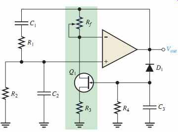
FIG. 11 Self-starting Wien-bridge oscillator using a JFET in the negative
feedback loop.
The Phase-Shift Oscillator
FIG. 13 shows a sinusoidal feedback oscillator called the phase-shift oscillator.
Each of the three RC circuits in the feedback loop can provide a maximum phase shift approaching 90°. Oscillation occurs at the frequency where the total phase shift through the three RC circuits is 180°. The inversion of the op-amp itself provides the additional 180° to meet the requirement for oscillation of a 360° (or 0°) phase shift around the feedback loop.
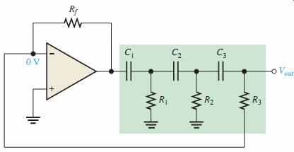
FIG. 13 Phase-shift oscillator.
The attenuation, B, of the three-section RC feedback circuit is

EQN. 3

EQN. 4
where B=R3/Rf. To meet the greater-than-unity loop gain requirement, the closed-loop voltage gain of the op-amp must be greater than 29 (set by and ). The frequency of oscillation is also derived on the companion website and is stated in the following equation, where R1 = R2 = R3 = R and C1 = C2 = C3 = C.
Twin-T Oscillator
Another type of RC feedback oscillator is called the twin-T because of the two T-type RC filters used in the feedback loop, as shown in FIG. 15(a). One of the twin-T filters has a low-pass response, and the other has a high-pass response. The combined parallel filters produce a band-stop or notch response with a center frequency equal to the desired frequency of oscillation, as shown in FIG. 15(b).
Oscillation cannot occur at frequencies above or below fr because of the negative feedback through the filters. At fr, however, there is negligible negative feedback; thus, the positive feedback through the voltage divider (R1 and R1) allows the circuit to oscillate.
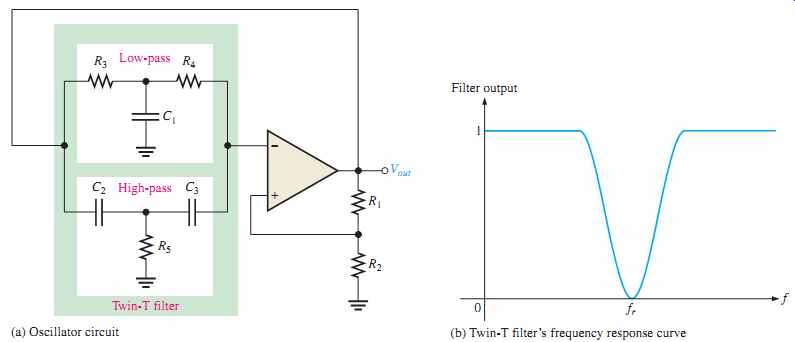
FIG. 15 Twin-T oscillator and twin-T filter response.
SECTION 3 CHECKUP
1. There are two feedback loops in the Wien-bridge oscillator. What is the purpose of each?
2. A certain lead-lag circuit has R1 = R2 and C1 = C2. An input voltage of 5 V rms is applied. The input frequency equals the resonant frequency of the circuit. What is the rms output voltage?
3. Why is the phase shift through the RC feedback circuit in a phase-shift oscillator 180°?
_4 OSCILLATORS WITH LC FEEDBACK CIRCUITS
Although the RC feedback oscillators, particularly the Wien bridge, are generally suitable for frequencies up to about 1 MHz, LC feedback elements are normally used in oscillators that require higher frequencies of oscillation. Also, because of the frequency limitation (lower unity-gain frequency) of most op-amps, discrete transistors (BJT or FET) are often used as the gain element in LC oscillators. This section introduces several types of resonant LC feedback oscillators: the Colpitts, Clapp, Hartley, Armstrong, and crystal-controlled oscillators.
After completing this section, you should be able to:
-- Describe and analyze the operation of LC feedback oscillators
-- Identify and analyze a Colpitts oscillator
-- Determine the resonant frequency
-- Describe the conditions for oscillation and start-up
-- Discuss and analyze loading of the feedback circuit
-- Identify and analyze a Clapp oscillator
-- Determine the resonant frequency
-- Identify and analyze a Hartley oscillator
-- Determine the resonant frequency and attenuation of the feedback circuit
-- Identify and analyze an Armstrong oscillator
-- Determine the resonant frequency
-- Describe the operation of crystal-controlled oscillators
-- Define piezoelectric effect
-- Discuss the quartz crystal
-- Discuss the modes of operation in the crystal
The Colpitts Oscillator
One basic type of resonant circuit feedback oscillator is the Colpitts, named after its inventor-as are most of the others we cover here. As shown in FIG. 16, this type of oscillator uses an LC circuit in the feedback loop to provide the necessary phase shift and to act as a resonant filter that passes only the desired frequency of oscillation.
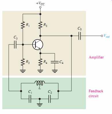
FIG. 16 A basic Colpitts oscillator with a BJT as the gain element.
The approximate frequency of oscillation is the resonant frequency of the LC circuit and is established by the values of C1, C2, and L according to this familiar formula:
EQN. 5
where C_T is the total capacitance. Because the capacitors effectively appear in series around the tank circuit, the total capacitance is
C_T = C1C2/C1+C2
Conditions for Oscillation and Start-Up The attenuation, B, of the resonant feedback circuit in the Colpitts oscillator is basically determined by the values of and FIG. 17 shows that the circulating tank current is through both and (they are effectively in series). The voltage developed across is the oscillator's output voltage and the voltage developed across is the feedback voltage as indicated. The expression for the attenuation (B) is […]
---p818
Cancelling the 2 pi fr terms gives Since B = C2/C1
As you know, a condition for oscillation is:
AvB = C1/C2
... where is the voltage gain of the amplifier, which is represented by the triangle in FIG. 17. With this condition met, Actually, for the oscillator to be self-starting, must be greater than 1 (that is, Therefore, the voltage gain must be made slightly greater than
Loading of the Feedback Circuit Affects the Frequency of Oscillation
As indicated in FIG. 18, the input impedance of the amplifier acts as a load on the resonant feed back circuit and reduces the Q of the circuit. The resonant frequency of a parallel resonant circuit depends on the Q, according to the following formula:
EQN. 7
As a rule of thumb, for a Q greater than 10, the frequency is approximately as stated in EQN. 5. When Q is less than 10, however, is reduced significantly.
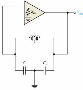
FIG. 18 Zin of the amplifier loads the feed back circuit and lowers its
Q, thus lowering the resonant frequency.
------------
HISTORY NOTE
Edwin H. Colpitts was involved in the development of oscillators and vacuum tube push-pull amplifiers at Western Electric in the early 1900s. Western Electric research laboratories became part of Bell Laboratories in 1925, and Colpitts became vice-president of Bell Labs before retirement. The Colpitts oscillator is named in his honor.
------------------
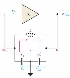
FIG. 17 The attenuation of the tank circuit is the output of the tank
(Vf) divided by the input to the tank (Vout). B _ Vf /Vout _ C2/C1. For
AvB _ 1, Av must be greater than C1/C2.
----------------
A FET can be used in place of a BJT, as shown in FIG. 19, to minimize the loading effect of the transistor's input impedance. Recall that FETs have much higher input impedances than do bipolar junction transistors. Also, when an external load is connected to the oscillator output, as shown in FIG. 20(a), fr may decrease, again be cause of a reduction in Q. This happens if the load resistance is too small. In some cases, one way to eliminate the effects of a load resistance is by transformer coupling, as indicated in FIG. 20(b).
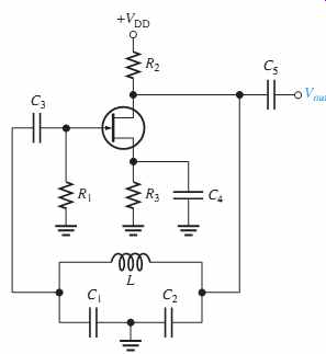
FIG. 19 A basic FET Colpitts oscillator.
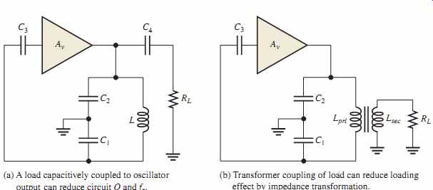
FIG. 20 Oscillator loading.
The Clapp Oscillator
The Clapp oscillator is a variation of the Colpitts. The basic difference is an additional capacitor, in series with the inductor in the resonant feedback circuit, as shown in FIG. 22. Since is in series with and around the tank circuit, the total capacitance is
---p821
and the approximate frequency of oscillation is:
---p821b
If C3 is much smaller than C1 and C2 then C3 almost entirely controls the resonant frequency.
Since and are both connected to ground at one end, the junction capacitance of the transistor and other stray capacitances appear in parallel with C1 and C2 to ground, altering their effective values. C3 is not affected, however, and thus provides a more accurate and stable frequency of oscillation.
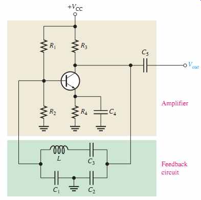
FIG. 22 A basic Clapp oscillator.
The Hartley Oscillator
The Hartley oscillator is similar to the Colpitts except that the feedback circuit consists of two series inductors and a parallel capacitor as shown in FIG. 23.
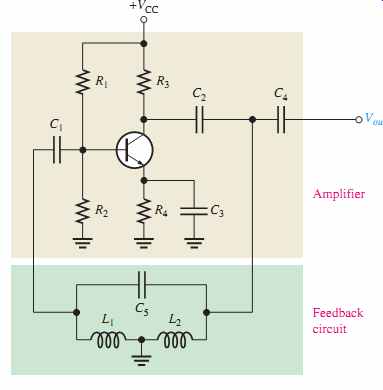
FIG. 23 A basic Hartley oscillator.
-------------
HISTORY NOTE
Ralph Vinton Lyon Hartley (1888-1970) invented the Hartley oscillator and the Hartley transform, a mathematical analysis method, which contributed to the foundations of information theory.
In 1915 he was in charge of radio receiver development for the Bell System transatlantic radiotelephone tests. During this time he developed the Hartley oscillator. A patent for the oscillator was filed in 1915 and awarded in 1920.
-------------
In this circuit, the frequency of oscillation for is Q > 10
fr = 1/2p _/L-T C
...where LT = L1 + L2. The inductors act in a role similar to C1 and C2 in the Colpitts to determine the attenuation, B, of the feedback circuit.
B _ L1 / L2
To assure start-up of oscillation, must be greater than 1/B.
Av = L2 / L1
EQN. 8
Loading of the tank circuit has the same effect in the Hartley as in the Colpitts; that is, the Q is decreased and thus decreases.
The Armstrong Oscillator
This type of LC feedback oscillator uses transformer coupling to feed back a portion of the signal voltage, as shown in FIG. 24. It is sometimes called a "tickler" oscillator in reference to the transformer secondary or "tickler coil" that provides the feedback to keep the oscillation going. The Armstrong is less common than the Colpitts, Clapp, and Hartley, mainly because of the disadvantage of transformer size and cost. The frequency of oscillation is set by the inductance of the primary winding (Lpri) in parallel with C1.

EQN. 9
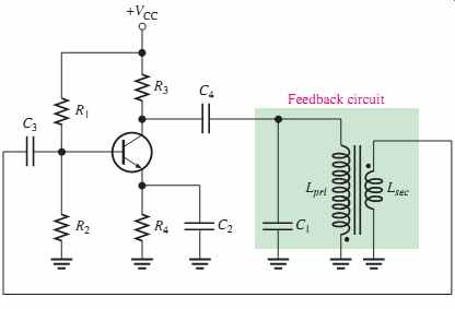
FIG. 24 A basic Armstrong oscillator.
-------------
HISTORY NOTE
Edwin Howard Armstrong (1890-1954) was an American electrical engineer and inventor. He was the inventor of the FM radio.
Armstrong also invented the regenerative circuit (patented 1914), the superheterodyne receiver (patented 1918) and the superregenerative circuit (patented 1922). Many of Armstrong's inventions were ultimately claimed by others in patent lawsuits. The Armstrong oscillator is named in his honor.
-------------
Crystal-Controlled Oscillators
The most stable and accurate type of feedback oscillator uses a piezoelectric crystal in the feedback loop to control the frequency.
The Piezoelectric Effect
Quartz is one type of crystalline substance found in nature that exhibits a property called the piezoelectric effect. When a changing mechanical stress is applied across the crystal to cause it to vibrate, a voltage develops at the frequency of mechanical vibration. Conversely, when an ac voltage is applied across the crystal, it vibrates at the frequency of the applied voltage. The greatest vibration occurs at the crystal's natural resonant frequency, which is determined by the physical dimensions and by the way the crystal is cut.
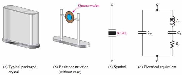
FIG. 25 A quartz crystal. --- (c) Symbol (a) Typical packaged crystal
(b) Basic construction (without case) (d) Electrical equivalent
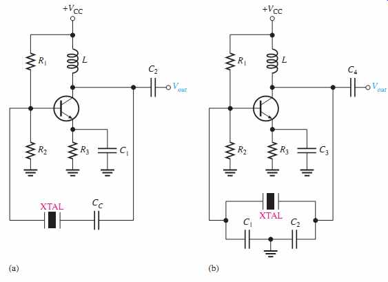
FIG. 26 Basic crystal oscillators.
Crystals used in electronic applications typically consist of a quartz wafer mounted be tween two electrodes and enclosed in a protective "can" as shown in FIG. 25(a) and (b).
A schematic symbol for a crystal is shown in FIG. 25(c), and an equivalent RLC circuit for the crystal appears in FIG. 25(d). As you can see, the crystal's equivalent circuit is a series-parallel RLC circuit and can operate in either series resonance or parallel resonance. At the series resonant frequency, the inductive reactance is cancelled by the reactance of Cs. The remaining series resistor Rs, determines the impedance of the crystal.
Parallel resonance occurs when the inductive reactance and the reactance of the parallel capacitance Cp, are equal. The parallel resonant frequency is usually at least 1 kHz higher than the series resonant frequency. A great advantage of the crystal is that it exhibits a very high Q (Qs with values of several thousand are typical).
An oscillator that uses a crystal as a series resonant tank circuit is shown in FIG. 26(a). The impedance of the crystal is minimum at the series resonant frequency, thus providing maximum feedback. The crystal tuning capacitor, CC, is used to "fine tune" the oscillator frequency by "pulling" the resonant frequency of the crystal slightly up or down.
FIG. 26 Basic crystal oscillators.
A modified Colpitts configuration is shown in FIG. 26(b) with a crystal acting as a parallel resonant tank circuit. The impedance of the crystal is maximum at parallel resonance, thus developing the maximum voltage across the capacitors. The voltage across C1 is fed back to the input.
Modes of Oscillation in the Crystal
Piezoelectric crystals can oscillate in either of two modes-fundamental or overtone. The fundamental frequency of a crystal is the lowest frequency at which it is naturally resonant. The fundamental frequency depends on the crystal's mechanical dimensions, type of cut, and other factors, and is inversely proportional to the thickness of the crystal slab. Because a slab of crystal cannot be cut too thin without fracturing, there is an upper limit on the fundamental frequency. For most crystals, this upper limit is less than 20 MHz. For higher frequencies, the crystal must be operated in the overtone mode. Overtones are approximate integer multiples of the fundamental frequency. The overtone frequencies are usually, but not always, odd multiples of (3,5,7,...) the fundamental. Many crystal oscillators are available in integrated circuit packages.
SECTION 4 CHECKUP
1. What is the basic difference between the Colpitts and the Hartley oscillators?
2. What is the advantage of a FET amplifier in a Colpitts or Hartley oscillator?
3. How can you distinguish a Colpitts oscillator from a Clapp oscillator?