AMAZON multi-meters discounts AMAZON oscilloscope discounts
cont. from part 1
5. INTEGRATED CIRCUIT VOLTAGE REGULATORS
In the previous sections, the basic voltage regulator configurations were presented.
Several types of both linear and switching regulators are available in integrated circuit (IC) form. Generally, the linear regulators are three-terminal devices that provide either positive or negative output voltages that can be either fixed or adjustable. In this section, typical linear and switching IC regulators are introduced.
After completing this section, you should be able to:
-- Discuss integrated circuit voltage regulators
-- Discuss fixed positive linear voltage regulators
-- Describe the 78XX regulators
-- Explain thermal overload
-- Discuss fixed negative linear voltage regulators
-- Describe the 79XX regulators
-- Discuss adjustable positive linear voltage regulators
-- Describe the LM317 regulator
-- Determine the output voltage
-- Discuss adjustable negative linear voltage regulators
-- Describe the LM337 regulator
-- Discuss switching voltage regulators
-- Describe the 78S40 regulator
Fixed Positive Linear Voltage Regulators
Although many types of IC regulators are available, the 78XX series of IC regulators is representative of three-terminal devices that provide a fixed positive output voltage. The three terminals are input, output, and ground as indicated in the standard fixed voltage configuration in FIG. 26(a). The last two digits in the part number designate the output voltage.
For example, the 7805 is a +5.0 V regulator. For any given regulator, the output voltage can be as much as 4% of the nominal output. Thus, a 7805 may have an output from 4.8 V to 5.2 V but will remain constant in that range. Other available output voltages are given in FIG. 26(b) and common packages are shown in part (c).
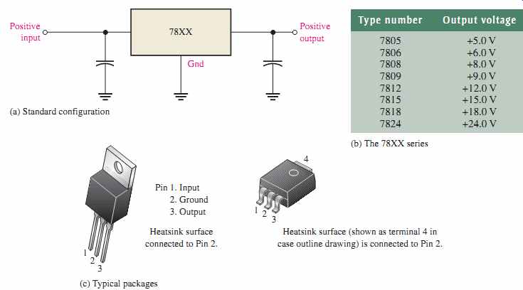
FIG. 26 The 78XX series three-terminal fixed positive voltage regulators.
Capacitors, although not always necessary, are sometimes used on the input and output as indicated in FIG. 26(a). The output capacitor acts basically as a line filter to improve transient response. The input capacitor filters the input and prevents unwanted oscillations when the regulator is some distance from the power supply filter such that the line has a significant inductance.
The 78XX series can produce output currents up to in excess of 1A when used with an adequate heat sink. The input voltage must be approximately 2.5 V above the output volt age in order to maintain regulation. The circuits have internal thermal overload protection and short-circuit current-limiting features. Thermal overload occurs when the internal power dissipation becomes excessive and the temperature of the device exceeds a certain value. Almost all applications of regulators require that the device be secured to a heat sink to prevent thermal overload.
Fixed Negative Linear Voltage Regulators
The 79XX series is typical of three-terminal IC regulators that provide a fixed negative out put voltage. This series is the negative-voltage counterpart of the 78XX series and shares most of the same features and characteristics except the pin numbers are different than the positive regulators. FIG. 27 indicates the standard configuration and part numbers with corresponding output voltages that are available.

FIG. 27 The 79XX series three-terminal fixed negative voltage regulators.
Adjustable Positive Linear Voltage Regulators
The LM317 is an example of a three-terminal positive regulator with an adjustable output voltage. The standard configuration is shown in FIG. 28. The capacitors are for de coupling and do not affect the dc operation. Notice that there is an input, an output, and an adjustment terminal. The external fixed resistor R1 and the external variable resistor R2 provide the output voltage adjustment. VOUT can be varied from 1.2 V to 37 V depending on the resistor values. The LM317 can provide over 1.5 A of output current to a load.
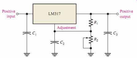
FIG. 28 The LM317 three-terminal adjustable positive voltage regulator.
The LM317 is operated as a "floating" regulator because the adjustment terminal is not connected to ground, but floats to whatever voltage is across R2. This allows the output voltage to be much higher than that of a fixed-voltage regulator.
Basic Operation
As indicated in FIG. 29, a constant 1.25 V reference voltage (VREF) is maintained by the regulator between the output terminal and the adjustment terminal. This constant reference voltage produces a constant current (IREF) through R1, regardless of the value of R2. IREF is also through R2.
R2.
[IREF = VREF R1 = 1.25 V R1]
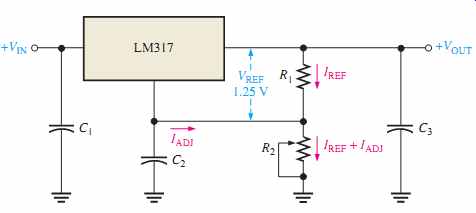
FIG. 29 Operation of the LM317 adjustable positive voltage regulator.
There is a very small constant current at the adjustment terminal of approximately 50 uA called which is through IADJ. A formula for the output voltage is developed as follows.
As you can see, the output voltage is a function of both R1 and R2. Once the value of R1 is set, the output voltage is adjusted by varying R2.
Adjustable Negative Linear Voltage Regulators
The LM337 is the negative output counterpart of the LM317 and is a good example of this type of IC regulator. Like the LM317, the LM337 requires two external resistors for output voltage adjustment as shown in FIG. 31. The output voltage can be adjusted from -37V to -1.2V depending on the external resistor values. The capacitors are for decoupling and do not affect the dc operation.
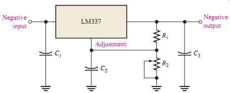
FIG. 31 The LM337 three-terminal adjustable negative voltage regulator.
Switching Voltage Regulators
There are many integrated circuit switching regulators available. The two used as typical examples are the ADP1612/ADP1613 step-up (boost) regulator and the ADP2300/ADP2301 step-down (buck) regulator. The basic operation was explained earlier in the Unit.
The Step-Up Switching Regulator
The step-up regulator configuration using an ADP1612/ADP1613 is shown in FIG. 32(a). The ADP1612 and the ADP1613 are essentially the same except for their switching frequency, which is used in the pulse-width modulation (PWM) operation.
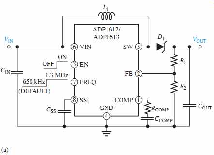
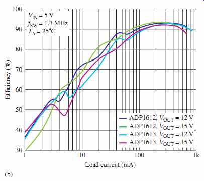
FIG. 32 Step-up configuration and efficiency vs. current graph.
This regulator operates with PWM and exhibits an efficiency of up to 94% at the higher switch frequency, depending on the output current and voltage, as shown by the graphs in FIG. 32(b). Notice that as the load current increases, the efficiency increases. The output voltage has a much smaller effect. The operating frequency of the PWM is pin selectable for 650 kHz or 1.3 MHz. The lower frequency results in better efficiency, and the higher frequency allows the use of smaller external components. For the 650 kHz operation, pin 7 (FREQ) is connected to ground or left open (floating for default). For the 1.3 MHz operation, pin 7 is connected to VIN (pin 6). The input voltage range is 1.8 V to 5.5 V and the output voltage can be as high as 20 V.
This device has thermal shutdown (TSD) protection in case the temperature exceeds 150°C and turns back on when the temperature drops to 130°C. Also, the under-voltage lock-out (UVLO) feature prevents erratic output voltages if the input voltage falls below a minimum value.
The capacitor connected to pin 8 (soft start) prevents a large inrush of current when the device is first turned on. The EN input (pin 3) turns the regulator on or off. The COMP input (pin 1) requires a series RC circuit for compensation. The FB input (pin 2) is connected to a voltage divider to provide feedback for output voltage control. An inductor is connected from the input to SW (switching output, pin 5), and a rectifier diode is connected from SW to the output voltage. Notice the diode in this case is a Schottky diode for faster switching.
The Step-Down Switching Regulator
The step-down regulator configuration using an ADP2300/ADP2301 is shown in FIG. 33(a). The ADP2300 and the ADP2301 are essentially the same except for their switching frequency. Unlike the ADP1612/ADP1613, this device does not have pin-selectable frequencies. Instead, each has a fixed internal oscillator with a frequency of 700 kHz for the ADP2300 and 1.4 MHz for the ADP2301.
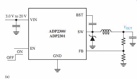
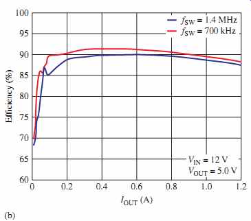
FIG. 33 Step-down configuration and efficiency vs. current graph.
This device has thermal shutdown (TSP) protection in case temperature exceeds 140°C and turns back on when the temperature drops to 150°C. Also, it has an under-voltage lock-out (UVLO) feature and short-circuit protection.
This regulator operates with PWM and exhibits an efficiency of up to 91%, depending on the output current, as shown by the graphs in FIG. 33(b) for each frequency. Notice that as the load current increases above about 0.2 A, the efficiency remains relatively constant (between about 91% and about 88%) and drops off a little as the output current increases. In this case, the output voltage is constant at 5 V. The input voltage range is 3 V to 20 V, and the output voltage can be as high as 20 V. The output voltage is from 0.8 x VIN to 0.85 x VIN.
The only input that is not on the step-up device is the BST (boot-strap). A capacitor must be connected from BST (pin 1) to SW (pin 6). The regulator generates a voltage for a MOSFET gate drive circuit by sensing a regulating voltage difference between the BST and SW pins.
SECTION 5 CHECKUP
1. What are the three terminals of a fixed-voltage regulator?
2. What is the output voltage of a 7809? Of a 7915?
3. What are the three terminals of an adjustable-voltage regulator?
4. What external components are required for a basic LM317 configuration?
6. INTEGRATED CIRCUIT VOLTAGE REGULATOR CONFIGURATIONS
In the last section, you saw several devices that are representative of the general types of IC voltage regulators. Now, several different ways these devices can be modified with external circuitry to improve or alter their performance are examined.
After completing this section, you should be able to
-- Describe applications of IC voltage regulators
-- Explain the purpose of an external pass transistor
-- Calculate the value of the external resistor required
-- Explain how current limiting can be implemented
-- Describe how to use a three-terminal regulator as a current regulator
-- Describe switching regulator configurations using the 78S40
-- Describe the step-down configuration
-- Describe the step-up configuration
The ExternalPass Transistor
As you know, an IC voltage regulator is capable of delivering only a certain amount of output current to a load. For example, the 78XX series regulators can handle a peak out put current of 1.3 A (more under certain conditions). If the load current exceeds the maximum allowable value, there will be thermal overload and the regulator will shut down. A thermal overload condition means that there is excessive power dissipation inside the device.
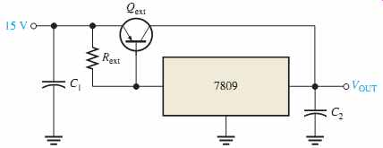
If an application requires more than the maximum current that the regulator can deliver, an external pass transistor Qext, can be used. FIG. 34 illustrates a three-terminal regulator with an external pass transistor for handling currents in excess of the output current capability of the basic regulator.
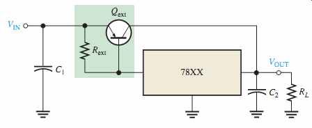
FIG. 34 A 78XX-series three-terminal regulator with an external pass transistor
to increase power dissipation.
The value of the external current-sensing resistor, Rext, determines the value of current at which Qext begins to conduct because it sets the base-to-emitter voltage of the transistor.
As long as the current is less than the value set by Rext, the transistor Qext is off, and the regulator operates normally as shown in FIG. 35(a). This is because the voltage drop across Rext is less than the 0.7 V base-to-emitter voltage required to turn Qext on. Rext is determined by the following formula, where Imax is the highest current that the voltage regulator is to handle internally.
When the current is sufficient to produce at least a 0.7 V drop across Rext, the external pass transistor Qext turns on and conducts any current in excess of Imax, as indicated in FIG. 35(b). Qext will conduct more or less, depending on the load requirements.
For example, if the total load current is 3 A and Imax was selected to be 1 A, the external pass transistor will conduct 2 A, which is the excess over the internal voltage regulator current Imax.
===============
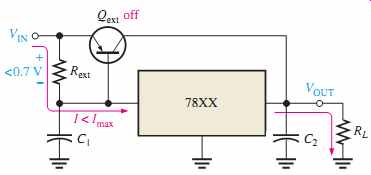
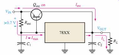
FIG. 35 Operation of the regulator with an external pass transistor.
(a) When the regulator current is less than Imax, the external pass transistor is off and the regulator is handling all of the current.
(b) When the load current exceeds Imax, the drop across Rext turns Qext on and it conducts the excess current.
==============
The external pass transistor is typically a power transistor with a heat sink that must be capable of handling a maximum power of
Pext = Iext(VIN - VOUT)
Current Limiting
A drawback of the circuit in FIG. 34 is that the external transistor is not protected from excessive current, such as would result from a shorted output. An additional current limiting circuit (Qlim and Rlim) can be added as shown in FIG. 36 to protect Qext from excessive current and possible burn out.
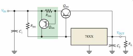
FIG. 36 Regulator with current limiting.
The following describes the way the current-limiting circuit works. The current-sensing resistor Rlim sets the VBE of transistor Qlim. The base-to-emitter voltage of Qext is now determined by VRext
VRlim because they have opposite polarities. So, for normal operation, the drop across Rext must be sufficient to overcome the opposing drop across Rlim. If the current through Qext exceeds a certain maximum (Iext(max)) because of a shorted output or a faulty load, the voltage across Rlim reaches 0.7 V and turns Qlim on. Qlim now conducts cur rent through the regulator and away from Qext, forcing a thermal overload to occur and shut down the regulator. Remember, the IC regulator is internally protected from thermal over load as part of its design.
This action is illustrated in FIG. 37. In part (a), the circuit is operating normally with Qext conducting less than the maximum current that it can handle with Qlim off. Part (b) shows what happens when there is a short across the load. The current through Qext suddenly increases and causes the voltage drop across Rlim to increase, which turns Qlim on. The current is now diverted through the regulator, which causes it to shut down due to thermal overload.
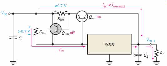
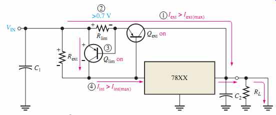
FIG. 37 The current-limiting action of the regulator circuit.
A Current Regulator
The three-terminal regulator can be used as a current source when an application requires that a constant current be supplied to a variable load. The basic circuit is shown in FIG. 38 where R1 is the current-setting resistor. The regulator provides a fixed constant voltage VOUT, between the ground terminal (not connected to ground in this case) and the out put terminal. This determines the constant current supplied to the load.
The current, IG, from the ground pin is very small compared to the output current and can often be neglected.
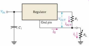
FIG. 38 The three-terminal regulator as a current source.
SECTION 6 CHECKUP
1. What is the purpose of using an external pass transistor with an IC voltage regulator?
2. What is the advantage of current limiting in a voltage regulator?
3. What does thermal overload mean?
============
Application Activity: Variable DC Power Supply
A regulated power supply with a fixed output voltage of was developed in Unit 3.
The company that manufactures this power supply plans to offer a new line of variable power supplies for which a specified voltage can be preset at the factory or can be adjusted by the user. In this application, the power supply with a variable regulator is developed to provide an output voltage from to and a maximum load current of 250 mA.
The Circuit
Recall that in the original power supply, a 7812 provided a regulated output. In this new power supply, a 7809 is used to produce that variable output voltage. As in the earlier design, it is recommended by the manufacturer that a capacitor be connected from the input terminal to ground and a capacitor be connected from the output terminal to ground, as shown in FIG. 40, to prevent high frequency oscillations and improve the performance. The reason for a small-value capacitor in parallel with a large one is that the large filter capacitor has an internal equivalent series resistance, which affects the high frequency response of the system. The effect is cancelled with the small capacitor.
The Transformer
The transformer must convert the 120 V rms line voltage to an ac voltage that will result in a rectified voltage that will produce when filtered.
34 V ; 10%
0.1 mF
0.33 mF
+12 V
+30 V +9V
+12 V
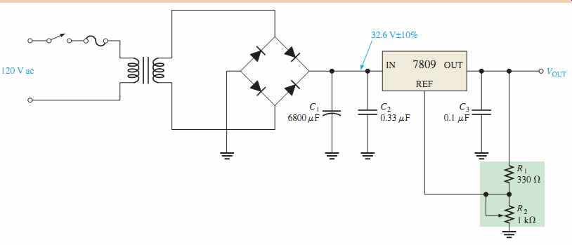
FIG. 40 Variable output power supply.
The Voltage Regulator
A partial datasheet for a 7809 is shown in FIG. 41. Notice that there is a range of nominal output voltages, but it is typically 9.0 V. The line and load regulations specify how much the output can vary about the nominal output value. For example, the typical 9.0 V output will change no more than 12 mV (typical) as the load current changes from 5 mA to 1.5 A. The output voltage of the regulator is the voltage between the output (OUT) terminal and the reference (REF) terminal. The voltage divider formed by R2 and R1 provides a reference voltage other than ground and increases the output voltage with respect to ground above the 9 V nominal regulator output by an amount equal to the voltage across R2.
1. What are the minimum and maximum nominal output voltages specified on the datasheet when IO is 500 mA.
2. From the datasheet, determine the maximum change in the output voltage when the load current changes from 5 mA to 1.5 A.
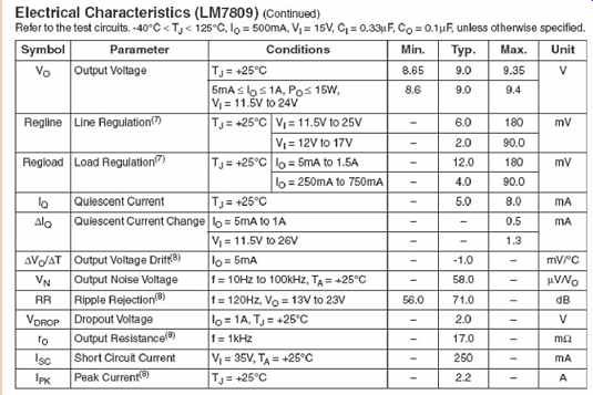
FIG. 41 Partial datasheet for a 7809 regulator. Copyright Fairchild Semiconductor
Corporation. Used by permission.
3. Calculate the maximum power dissipation in R1.
4. Calculate the maximum power dissipation in R2.
The Fuse The fuse will be in series with the primary winding of the transformer, as shown in FIG. 40. The fuse should be calculated based on the maximum allowable primary current. Recall from your dc/ac circuits course that if the voltage is stepped down, the current is stepped up. From the specifications for the unregulated power supply, the maximum load current is 100 mA.
5. Calculate the primary current and use this value to select a fuse rating for the circuit in FIG. 40.
Simulation
Multisim is used to simulate this power supply circuit. FIG. 42 shows the simulated regulated power supply circuit adjusted to show that it meets or exceeds the specified minimum and maximum output voltages.
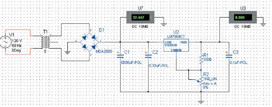
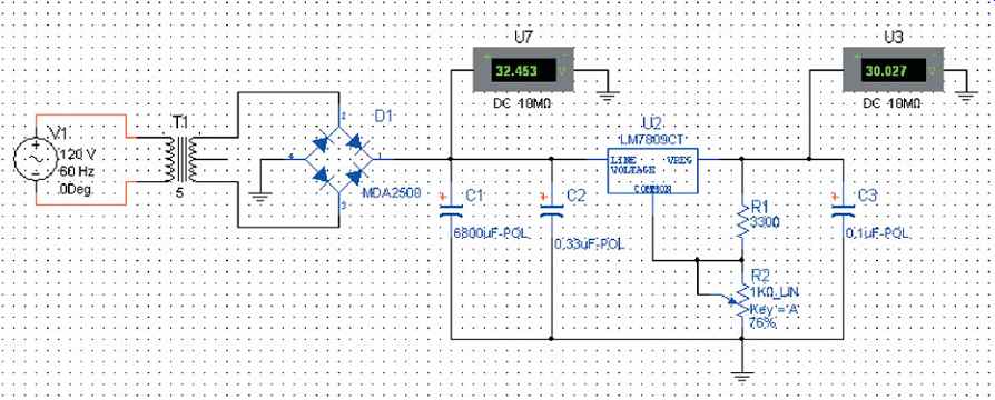
FIG. 42 Simulation of the regulated variable power supply circuit at the
minimum and maximum specified output voltages.
Build and simulate the circuit using your Multisim software. Verify the operation.
Lab Experiment
Printed Circuit Board
The variable regulated power supply prototype has been built and tested. It is now com mitted to a printed circuit layout, as shown in FIG. 43. Notice that a heat sink is used with the regulator IC to increase its ability to dissipate power. The output voltage is measured at the potentiometer.
6. Compare the printed circuit board to the schematic in FIG. 40.
7. Calculate the power dissipated by the regulator for an output of 9 V and IL = 100 mA.
8. Calculate the power dissipated by the regulator for an output of 30 V and IL = 100 mA.
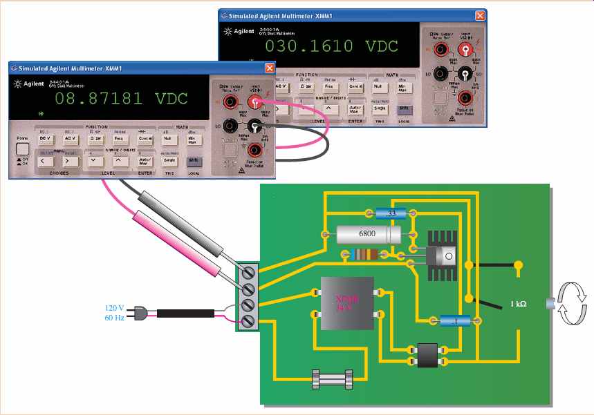
FIG. 43 Regulated power supply PC board adjusted for output voltages
that meet the minimum and maxi mum specifications.
SUMMARY
SECTION 1
Voltage regulators keep a constant dc output voltage when the input or load varies within limits.
-- Line regulation is the percentage change in the output voltage for a given change in the input voltage of a regulator.
-- Load regulation is the percentage change in output voltage for a given change in load current.
SECTION 2
A basic voltage regulator consists of a reference voltage source, an error detector, a sampling element, and a control device. Protection circuitry is also found in most regulators.
-- Two basic categories of voltage regulators are linear and switching.
-- Two basic types of linear regulators are series and shunt.
-- In a linear series regulator, the control element is a transistor in series with the load.
SECTION 3
In a linear shunt regulator, the control element is a transistor in parallel with the load.
SECTION 4
Three configurations for switching regulators are step-down, step-up, and inverting.
-- Switching regulators are more efficient than linear regulators and are particularly useful in low-voltage, high-current applications.
SECTION 5
Three-terminal linear IC regulators are available for either fixed output or variable output voltages of positive or negative polarities.
-- The 78XX series are three-terminal IC regulators with fixed positive output voltage.
-- The 79XX series are three-terminal IC regulators with fixed negative output voltage.
-- The LM317 is a three-terminal IC regulator with a positive variable output voltage.
-- The LM337 is a three-terminal IC regulator with a negative variable output voltage.
SECTION 6
-- An external pass transistor increases the current capability of a regulator.
TERMS
Linear regulator--A voltage regulator in which the control element operates in the linear region.
Line regulation--The percentage change in output voltage for a given change in input (line) voltage.
Load regulation--The percentage change in output voltage for a given change in load current from no load to full load.
Regulator--An electronic circuit that maintains an essentially constant output voltage with a changing input voltage or load current.
Switching regulator--A voltage regulator in which the control element operates as a switch.
Thermal overload--A condition in a rectifier where the internal power dissipation of the circuit exceeds a certain maximum due to excessive current.
FORMULAS
Voltage Regulation
Line regulation as a percentage
Line regulation in %/V
Percent load regulation
Load regulation in terms of output resistance and full-load resistance
Basic Series Regulator
Regulator output
For constant-current limiting (silicon)
Basic Shunt Regulator
Maximum load current
Basic Switching Regulators
For step-down switching regulator
Integrated Circuit Voltage Regulators
IC regulator
For external pass circuit
Regulator as a current source
TRUE or FALSE
1. Line regulation is a measure of how constant the output voltage is for a given change in the input voltage.
2. Load regulation depends on the amount of power dissipated in the load.
3. Linear and switching are two main categories of voltage regulators.
4. Two types of linear regulator are series and bypass.
5. Three types of switching regulator are step-down, step-up, and inverting.
6. The three terminals of a 78XX series regulator are input, output, and control.
7. An external bypass transistor is sometimes used to increase the current capability of a regulator.
8. Current limiting is used to protect the external bypass transistor.
9. The purpose of a heat sink is to help the regulator dissipate excessive heat.
10. A variable pulse-width modulator is part of a linear voltage regulator.
CIRCUIT-ACTION QUIZ
1. If the input voltage in FIG. 7 is increased by 1 V, the output voltage will (a) increase (b) decrease (c) not change
2. If the zener diode in FIG. 7 is changed to one with a zener voltage of 6.8 V, the output voltage will (a) increase (b) decrease (c) not change
3. If in FIG. 7 is increased in value, the output voltage will (a) increase (b) decrease (c) not change
4. If in FIG. 9 is reduced, the amount of current that the regulator can supply to the load will (a) increase (b) decrease (c) not change R4 R3
5. If in FIG. 15 is increased, the power dissipation in will (a) increase (b) decrease (c) not change
6. If the duty cycle of the variable pulse-width modulator in FIG. 17 is increased, the output voltage will (a) increase (b) decrease (c) not change
7. If in FIG. 30 is adjusted to a lower value, the output voltage will (a) increase (b) decrease (c) not change
8. To increase the maximum current that the regulator in FIG. 35 can supply, the value of must (a) increase (b) decrease (c) not change
Rext R2 R1 R2
SELF-TEST
SECTION 1.
In the case of line regulation, (a) when the temperature varies, the output voltage stays constant (b) when the output voltage changes, the load current stays constant (c) when the input voltage changes, the output voltage stays constant (d) when the load changes, the output voltage stays constant
2. In the case of load regulation, (a) when the temperature varies, the output voltage stays constant (b) when the input voltage changes, the load current stays constant (c) when the load changes, the load current stays constant (d) when the load changes, the output voltage stays constant
3. All of the following are parts of a basic voltage regulator except (a) control element (b) sampling circuit (c) voltage-follower (d) error detector (e) reference voltage
SECTION 2:
4. The basic difference between a series regulator and a shunt regulator is (a) the amount of current that can be handled (b) the position of the control element (c) the type of sample circuit (d) the type of error detector
5. In a basic series regulator, is determined by (a) the control element (b) the sample circuit (c) the reference voltage (d) answers (b) and (c)
6. The main purpose of current limiting in a regulator is (a) protection of the regulator from excessive current (b) protection of the load from excessive current (c) to keep the power supply transformer from burning up (d) to maintain a constant output voltage
7. In a linear regulator, the control transistor is conducting (a) a small part of the time (b) half the time (c) all of the time (d) only when the load current is excessive
SECTION 3:
8. In a basic shunt regulator, is determined by (a) the control element (b) the sample circuit (c) the reference voltage (d) answers (b) and (c)
SECTION 4
9. In a switching regulator, the control transistor is conducting (a) part of the time (b) all of the time (c) only when the input voltage exceeds a set limit (d) only when there is an overload
VOUT VOUT
SECTION 5
10. The LM317 is an example of an IC (a) three-terminal negative voltage regulator (b) fixed positive voltage regulator (c) switching regulator (d) linear regulator (e) variable positive voltage regulator (f) answers (b) and (d) only (g) answers (d) and (e) only SECTION 6
11. An external pass transistor is used for (a) increasing the output voltage (b) improving the regulation (c) increasing the current that the regulator can handle (d) short-circuit protection
PROBLEMS
Answers to all odd-numbered problems are at the end of the guide.
BASIC PROBLEMS
SECTION 1
Voltage Regulation
1. The nominal output voltage of a certain regulator is 8 V. The output changes 2 mV when the input voltage goes from 12 V to 18 V. Determine the line regulation and express it as a percent age change over the entire range of
2. Express the line regulation found in Problem 1 in units of %/V.
3. A certain regulator has a no-load output voltage of 10 V and a full-load output voltage of 9.90 V.
What is the percent load regulation?
4. In Problem 3, if the full-load current is 250 mA, express the load regulation in %/mA.
SECTION 2
Basic Linear Series Regulators
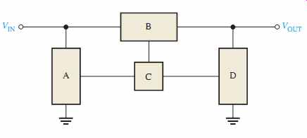
5. Label the functional blocks for the voltage regulator in FIG. 44.
VIN.
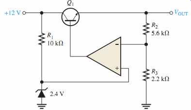
6. Determine the output voltage for the regulator in FIG. 45.
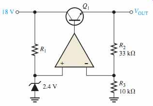
FIG. 45 Multisim file circuits are identified with a logo and are in
the Problems folder on the companion website.
Filenames correspond to figure numbers (e.g., Fig. 45).
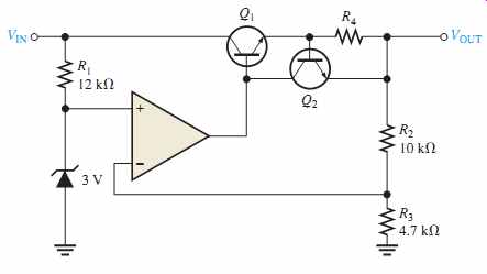
7. Determine the output voltage for the series regulator in FIG. 46.
8. If R3 in FIG. 46 is increased to 4.7 k OHM what happens to the output voltage?
9. If the zener voltage is 2.7 V instead of 2.4 V in FIG. 46, what is the output voltage?
10. A series voltage regulator with constant-current limiting is shown in FIG. 47. Determine the value of R4 if the load current is to be limited to a maximum value of 250 mA. What power rating must R4 have?
11. If R4 the determined in Problem 10 is halved, what is the maximum load current?
SECTION 3
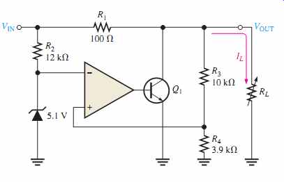
Basic Linear Shunt Regulators 12. In the shunt regulator of FIG. 48, when the load current increases, does Q1 conduct more or less? Why?
13. Assume IL remains constant and changes by 1 V in FIG. 48. What is the change in the collector current of Q1.
14. With a constant input voltage of 17 V, the load resistance in FIG. 48 is varied from 1k OHM to 1.2 k OHM. Neglecting any change in output voltage, how much does the shunt current through Q1 change?
15. If the maximum allowable input voltage in FIG. 48 is 25 V, what is the maximum possible output current when the output is short-circuited? What power rating should R1 have?
SECTION 4
Basic Switching Regulators
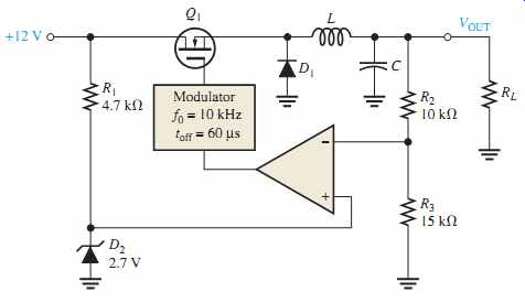
16. A basic switching regulator is shown in FIG. 49. If the switching frequency of the transistor is 10 kHz with an off-time of 60 u-s, what is the output voltage?
17. What is the duty cycle of the transistor in Problem 16?
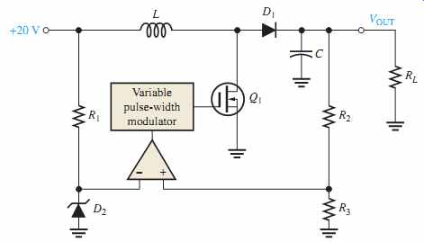
18. When does the diode in FIG. 50 become forward-biased? D1
19. If the on-time of Q1 in FIG. 50 is decreased, does the output voltage increase or decrease?
SECTION 5
Integrated Circuit Voltage Regulators
20. What is the output voltage of each of the following IC regulators? (a) 7806 (b) 7905.2 (c) 7818 (d) 7924
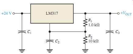
21. Determine the output voltage of the regulator in FIG. 51. IADJ = 50 uA.
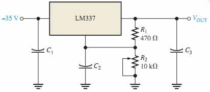
22. Determine the minimum and maximum output voltages for the circuit in FIG. 52. IADJ = 50 mA.
23. With no load connected, how much current is there through the regulator in FIG. 51? Neglect the adjustment terminal current.
24. Select the values for the external resistors to be used in an LM317 circuit that is required to produce an output voltage of 12V with an input of 18 V. The maximum regulator current with no load is to be 2 mA. There is no external pass transistor.
SECTION 6
Integrated Circuit Voltage Regulator Configurations
25. In the regulator circuit of FIG. 53, determine Rext if the maximum internal regulator cur rent is to be 250 mA.
26. Using a 7812 voltage regulator and a 10 OHM load in FIG. 53, how much power will the external pass transistor have to dissipate? The maximum internal regulator current is set at 500 mA by Rext.
27. Show how to include current limiting in the circuit of FIG. 53. What should the value of the limiting resistor be if the external current is to be limited to 2A?
28. Using an LM317, design a circuit that will provide a constant current of 500 mA to a load.
29. Repeat Problem 28 using a 7908.
30. How do you set up the ADP1612/1613 switching regulator for a switching frequency of 1.3 MHz?


