AMAZON multi-meters discounts AMAZON oscilloscope discounts
Cont. from part a
Transistors
The transistor is a three-terminal semiconductor device commonly used to amplify a signal or switch a circuit on and off. Amplification is the process of taking a small signal and increasing the signal size. Transistors are used as switches in electric motor drives to control the voltage and current applied to motors. Transistors are capable of extremely fast switching with no moving parts. There are two general types of transistors in use today: the bipolar transistor (often referred to as a bipolar junction transistor, or BJT) and the field-effect transistor (FET). Another common use of transistors is as part of integrated circuits (ICs). As an example, a computer microprocessor chip may contain as many as 3.5 million transistors.
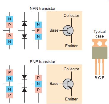
Ill. 13 Bipolar junction transistor (BJT). NPN transistor; Collector;
PNP transistor; Typical case: Collector, Base, Emitter
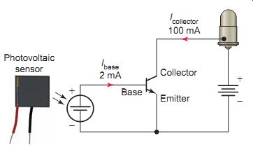
Ill. 14 BJT current amplification. Photovoltaic sensor;
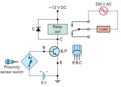
Ill. 15 BJT switching of an AC load.
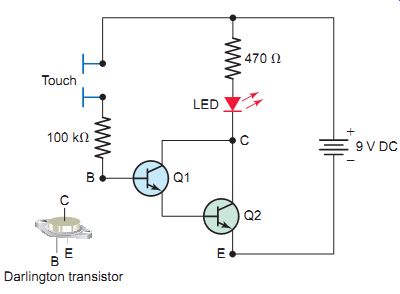
Ill. 16 Darlington transistor as part of a touch-switch circuit. Darlington
transistor; Proximity sensor switch;
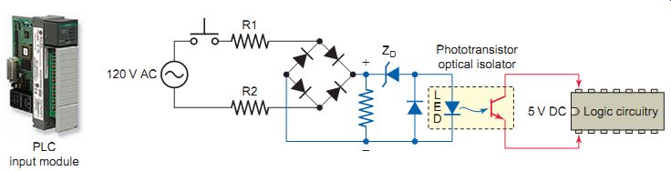
Ill. 17 Phototransistor employed as part of an optical isolator found
in a programmable logic controller (PLC) AC input module circuit. PLC
input module; Phototransistor optical isolator; Logic circuitry
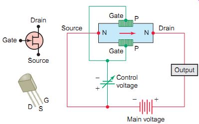
Ill. 18 Junction field-effect transistor (JFET). Main voltage; Output;
Control voltage; Drain, Source, Gate
Bipolar Junction Transistor (BJT)
In their most basic form, bipolar transistors essentially consist of a pair of PN junction diodes that are joined back to back as illustrated in Ill. 13. It consists of three sections of semiconductors: an emitter (E), a base (B) and a collector (C). The base region is very thin, so a small current in this region can be used to control a larger current flowing between the base and collector regions There are two types of standard BJT transistors, NPN and PNP, with different circuit symbols. The letters refer to the layers of semiconductor material used to make the transistor. NPN and PNP transistors operate in a similar manner, their biggest difference being the direction of current flow through the collector and emitter. Bipolar transistors are so named because the controlled current must go through two types of semi conductor material, P and N.
The BJT is a current amplifier in that a current flow from the base to the emitter results in a larger flow from the collector to the emitter. This, in effect, is current amplification, with the current gain known as the beta of the transistor. The circuit shown in Ill. 14 illustrates the way in which a BJT is used as a current amplifier to amplify the small current signal from a photovoltaic sensor. The operation of the circuit can be summarized as follows:
• The transistor is connected to two different DC voltage sources: the supply voltage and the voltage generated by the photovoltaic sensor when exposed to light.
• These voltage supplies are connected so that the base-emitter junction is forward-biased and the collector-emitter junction is reverse-biased,
• Current in the base lead is called the base current, and current in the collector lead is called the collector current.
• It’s called the common-emitter transistor configuration because both the base and collector circuits share the emitter lead as a common connection point.
• The amount of base current determines the amount of collector current.
• With no base current-that is, no light shining on the photovoltaic sensor-there is no collector cur rent (normally off).
• A small increase in base current, generated by the photovoltaic sensor, results in a much larger increase in collector current; thus, the base current acts to control the amount of collector current.
• The current amplification factor, or gain, is the ratio of the collector current to the base current; in this case 100 mA divided by 2 mA, or 50.
When a transistor is used as a switch, it has only two operating states, on and off. Bipolar transistors cannot directly switch AC loads and they are not usually a good choice for switching higher voltages or currents. In these cases a relay in conjunction with a low-power transistor is often used. The transistor switches current to the relay coil while the coil contacts switch current to the load. The circuit shown in Ill. 15 illustrates the way in which a BJT is used to control an AC load. The operation of the circuit can be summarized as follows:
• A low-power transistor is used to switch the current for the relay's coil.
• With the proximity switch open, no base or collector current flows, so the transistor is switched off. The relay coil will be deenergized and voltage to the load will be switched off by the normally open relay contacts.
• When the transistor is in the off state, the collector current is zero, the voltage drop across the collector and emitter is 12 V, and the voltage across the relay coil is 0 V.
• The proximity sensor switch, on closing, establishes a small base current that drives the collector fully on to the point where it’s said to be saturated, as it cannot pass any more current.
• The relay coil is energized and its normally open contacts close to switch on the load.
• When the transistor is in the on state, collector cur rent is at its maximum value and the voltage across the collector and emitter drops to near zero while that across the relay coil increases to approximately 12 V.
• The clamping diode prevents the induced voltage at turnoff from becoming high enough to damage the transistor.
The Darlington transistor (often called a Darlington pair) is a semiconductor device that combines two bipolar transistors in a single device so that the current amplified by the first transistor is amplified further by the second. The overall current gain is equal to the two individual transistor gains multiplied together. Ill. 16 shows the Darling ton transistor as part of a resistance touch-switch circuit.
The operation of the circuit can be summarized as follows:
• The Darlington pairs are packaged with three legs, like a single transistor.
• The base of transistor Q1 is connected to one of the electrodes of the touch switch.
• Placing your finger on the touch plate allows a small amount of current to pass through the skin and establish current flow through the base circuit of Q1 and drive it into saturation.
• The current amplified by Q1 is amplified further by Q2 to switch the LED on.
Like junction diodes, bipolar junction transistors are light-sensitive. Phototransistors are designed specifically to take advantage of this fact. The most common phototransistor is an NPN bipolar transistor with a light-sensitive collector-base PN junction. When this junction is exposed to light it creates a control current flow that switches the transistor on. Photodiodes also can provide a similar function, but at a much lower gain. Ill. 17 shows a phototransistor employed as part of an optical isolator found in a programmable logic controller (PLC) AC input module circuit. The operation of the circuit can be summarized as follows:
• When the push button is closed, 120 V AC is applied to the bridge rectifier through resistors R1 and R2.
• This produces a low-level DC voltage that is applied across the LED of the optical isolator.
• The zener diode (ZD) voltage rating sets the mini mum level of voltage that can be detected.
• When light from the LED strikes the phototransistor, it switches into conduction and the status of the push button is communicated in logic, or low-level DC voltage, to the processor.
• The optical isolator not only separates the higher AC input voltage from the logic circuits but also prevents damage to the processor by line voltage transients.
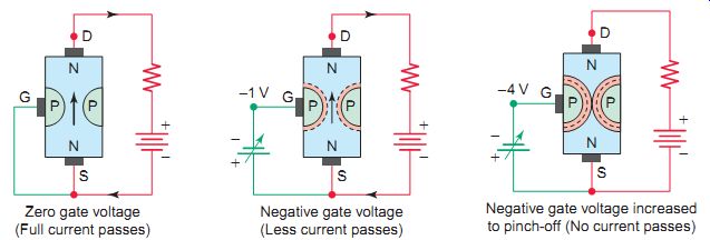
Ill. 19 Gate voltage control of current. Zero gate voltage (Full current
passes); Negative gate voltage (Less current passes); Negative gate voltage
increased to pinch-off (No current passes)
Field-Effect Transistor
The bipolar junction transistor is a current-controlled device, while the field-effect transistor (FET) is a voltage controlled device. The field-effect transistor uses basically no input current. Instead, output current flow is controlled by a varying electric field , which is created through the application of a voltage. This is the origin of the term field effect . The field-effect transistor was designed to get around the two major disadvantages of the bipolar junction transistor: low switching speed and high drive power, which are imposed by the base current.
The junction field-effect transistor (JFET) is shown in Ill. 18. It’s constructed with a bar of N-type material and a gate of P-type material. Because the material in the channel is N type, the device is called an N-channel JFET. JFETs have three connections, or leads: source, gate, and drain. These correspond to the emitter, base, and collector of the bipolar transistor, respectively. The names of the terminals refer to their functions. The gate terminal may be thought of as controlling the opening and closing of a physical gate. This gate permits electrons to flow through or blocks their passage by creating or eliminating a channel between the source and drain. Field-effect transistors are unipolar; their working current flows through only one type of semiconductor material. This is in contrast to bipolar transistors, which have current flowing through both N-type and P-type regions. There are also P-channel JFETs that use P-type material for the channel and N-type material for the gate. The main difference between the N- and P-types is that the polarities of voltage they are connected to are opposite.
The JFET operates in the depletion mode, which means it’s normally on. If a source of voltage is connected to the source and drain, and no source of voltage is connected to the gate, current is free to flow through the channel.
Ill. 19 illustrates the gate voltage control of current through an N-channel JFET. The operation of the circuit can be summarized as follows:
• The normal polarities for biasing the N-channel JFET are as indicated. Note that the JFET is normally operated with the control voltage connected to the source and gate junction in reverse bias. The result is very high input impedance.
• If a source voltage is connected to the source and drain, and no control voltage is connected to the gate, electrons are free to flow through the channel.
• A negative voltage connected to the gate increases the channel resistance and reduces the amount of current flow between the source and the drain.
• Thus, the gate voltage controls the amount of drain cur rent, and the control of this current is almost powerless.
• Continuing to increase the negative gate voltage to the pinch-off point will reduce the drain current to a very low value, effectively zero.
Metal Oxide Semiconductor Field-Effect Transistor (MOSFET)
The metal oxide semiconductor field-effect transistor (MOSFET) is by far the most common field-effect transistor. Field-effect transistors don’t require any gate current for operation so the gate structure can be completely insulated from the channel. The gate of a JFET consists of a reverse-biased junction, whereas the gate of a MOSFET consists of a metal electrode insulated by metal oxide from the channel. The insulated gate of a MOSFET has much higher input impedance than the JFET, so it’s even less of a load on preceding circuits.
Because the oxide layer is extremely thin, the MOSFET is susceptible to destruction by electrostatic charges.
Special precautions are necessary when handling or transporting MOS devices.
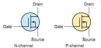
The MOSFET can be made with a P channel or an N channel. The action of each is the same, but the polarities are reversed. In addition, there are two types of MOSFETs: depletion-mode MOSFETs, or D type, and enhancement-mode MOSFETs, or E type. Symbols used for N- and P-channel depletion-mode MOSFETs are shown in Ill. 20. The channel is represented as a solid line to signify that the circuit between the drain and source is normally complete and that the device is normally on.
Gate voltage in a MOSFET circuit can be of either polarity, since a diode junction is not used. This makes the enhancement mode of operation possible. The enhancement-mode MOSFET is normally off, which means that if a voltage is connected to the drain and source and no voltage is connected to the gate, there will be no current flow through the device. The proper gate voltage will attract carriers to the gate region and form a conductive channel.
Thus the channel is considered to be "enhanced," or aided by gate voltage. Ill. 21 shows the schematic symbols used for enhancement-mode MOSFETs. Note that, unlike the depletion mode symbols, the line from the source to drain is broken. This implies that the device is normally off.
Ill. 20 Depletion-mode MOSFETs. N-channel; P-channel
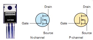
Ill. 21 Enhancement-mode
MOSFETs.
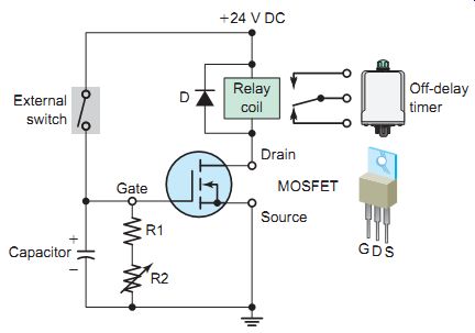
Ill. 22 MOSFET off-delay timer circuit.
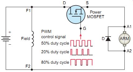
Ill. 23 Power MOSFET used as part of a chopper circuit.
Ill. 22 shows an enhancement-mode MOSFET used as part of an off-delay cube timer circuit. Because the gate current flow is negligible, a broad range of time-delay periods, from minutes to hours, is possible.
The operation of the circuit can be summarized as follows:
• With the switch initially open, a voltage is applied between the drain and source but no voltage is applied between the gate and source. Therefore, no current flows through the MOSFET and the relay coil will be deenergized.
• Closing the switch results in a positive volt age being applied to the gate, which triggers the
MOSFET into conduction to energize the relay coil and switch the state of its contacts.
• At the same time the capacitor is charged to 12 V DC.
• The circuit remains in this state with the relay coil energized as long as the switch remains closed.
• When the switch is opened, the timing action begins.
• The positive gate circuit to the 12-V source is opened.
• The stored positive charge of the capacitor keeps the MOSFET switched on.
• The capacitor begins to discharge its stored energy through R1 and R2 while still maintaining a positive voltage at the gate.
• The MOSFET and relay coil continue to conduct a current for as long as it takes the capacitor to discharge.
• The discharge rate, and thus the off-delay timing period, is adjusted by varying the resistance of R2.
Increasing the resistance will slow the rate of discharge and increase the timing period. Decreasing the resistance will have the opposite effect.
Power MOSFETs that are designed to handle larger amounts of current are used in some electronic DC motor speed controllers. For this type of application, the MOSFET is used to switch the applied DC voltage on and off very rapidly. The speed of a DC motor is directly proportional to the voltage applied to the armature. By switching the DC motor line voltage, it’s possible to control the average voltage applied to the motor armature.
Ill. 23 shows an enhancement-mode power MOS FET used as part of a chopper circuit. In this circuit the source voltage is chopped by the MOSFET to produce an average voltage somewhere between 0 and 100 percent of the DC supply voltage. The operation of the circuit can be summarized as follows:
• The DC supply and motor field voltage is fixed and the voltage applied to the motor armature is varied by the MOSFET using a technique called pulse width modulation (PWM).
• Pulse-width modulation works by applying a series of modulated square wave pulses to the gate.
• Motor speed is controlled by driving the motor with short pulses. These pulses vary in duration to change the speed of the motor. The longer the pulses, the faster the motor runs and vice versa.
• By adjusting the duty cycle of the gate signal (modulating the width of the pulse), the time fraction that the MOSFET is on can be varied, along with the average voltage to the motor armature and hence the motor speed.
• The diode (sometimes called a freewheeling diode) is connected in reverse bias to provide a discharge path for the collapsing magnetic field when voltage to the motor armature is switched off.
Insulated-Gate Bipolar Transistor (IGBT)
The insulated-gate bipolar transistor (IGBT) is a cross between a bipolar transistor and MOSFET in that it combines the positive attributes of both. BJTs have lower on resistance, but have longer switching times, especially at turn-off. MOSFETs can be turned on and off much faster, but their on-state resistance is higher.
IGBTs have lower on-state power loss in addition to faster switching speeds, allowing the electronic motor drive to operate at much higher switching frequencies and control more power.
The two different schematic symbols used to represent an N-type IGBT and its equivalent circuit are shown in Ill. 24. Notice that the IGBT has a gate like a MOS FET yet it has an emitter and a collector like a BJT. The equivalent circuit is depicted by a PNP transistor, where the base current is controlled by a MOS transistor. In essence, the IGFET controls the base current of a BJT, which handles the main load current between collector and emitter. This way, there is extremely high current gain (since the insulated gate of the IGFET draws practically no current from the control circuitry), but the collector-to emitter voltage drop during full conduction is as low as that of an ordinary BJT.
As applications for IGBT components have continued to expand rapidly, semiconductor manufacturers have responded by providing IGBTs in both discrete (individual) and modular packages. Ill. 25 shows a power electronic module that houses two insulated-gate bipolar power transistors and corresponding diodes. This package provides an easy way to cool the devices and to connect them to the outer circuit.
Ill. 26 illustrates how IGBTs are used in an electronic variable-frequency AC motor drive. A variable frequency drive controls the speed of the AC motor by varying the frequency supplied to the motor. In addition, the drive also regulates the output voltage in proportion to the output frequency to provide a relatively constant ratio of voltage to frequency (V/Hz), as required by the characteristics of the AC motor to produce adequate torque. The six IGBTs are capable of very high switching speeds and may be required to switch the voltage to the motor thou sands of times per second. The operation of the circuit can be summarized as follows:
• The input section of the drive is the converter. It contains six diodes, arranged in an electrical bridge. The diodes convert the three-phase AC power to DC power.
• The next section-the DC bus-sees a fixed DC voltage.
• The inductor (L) and the capacitor (C) work together to filter out any AC component of the DC waveform. The smoother the DC waveform, the cleaner the output waveform from the drive.
• The DC bus feeds the inverter, the final section of the drive. As the name implies, this section inverts DC voltage back to AC. But it does so in a variable voltage and frequency output.
• Fairly involved control circuitry coordinates the switching of the IGBT devices, typically through a logic control board that dictates the firing of power components in proper sequence.
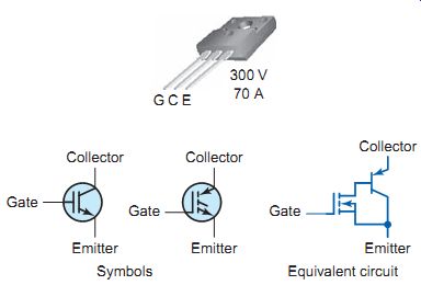
Ill. 24 Insulated-gate bipolar transistor (IGBT)-N type.
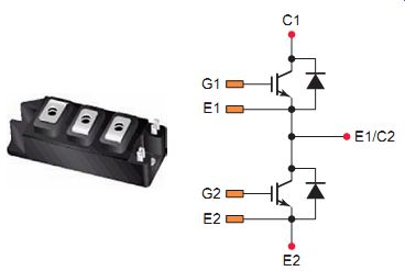
Ill. 25 Insulated-gate bipolar transistor (IGBT) power module.
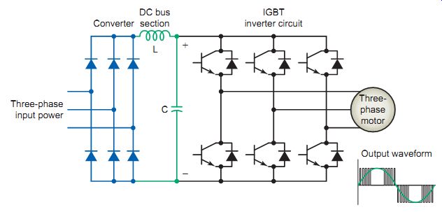
Ill. 26 IGBTs used in an electronic motor drive. Three-phase input power;
Converter, DC bus section, IGBT inverter circuit; Three-phase motor; Output
waveform
QUIZ
1. Explain the two main functions of a transistor.
2. What are the two general types of transistor?
3. Give a brief explanation of how current flow through a bipolar junction transistor is controlled.
4. State the two types of bipolar transistors.
5. What names are used to identify the three leads of a BJT?
6. Explain the term current gain as it applies to a BJT.
7. Describe the makeup of a Darlington transistor.
8. Give a brief explanation of how current flow through a phototransistor is controlled.
9. How is current flow through a field-effect transistor controlled?
10. State two advantages of field-effect transistors over bipolar types.
11. What names are used to identify the three leads of a junction field-effect transistor?
12. What is the main difference between the operation of N-channel and P-channel JFETs?
13. Why are field-effect transistors said to be unipolar?
14. JFETs are characterized as being "normally on." What does this mean?
15. Compare the gate structure of a JFET and a MOSFET.
16. In what way is the operation of a depletion-mode MOSFET different from that of an enhancement mode MOSFET?
17. Give a brief explanation of how a power MOSFET is operated as a chopper in a DC electronic motor drive.
18. How is current flow through an insulated-gate bipolar transistor controlled?
19. What names are used to identify the three leads of an IGBT?
20. What features of the IGBT make it the transistor of choice for power electronic motor control applications?
21. What are the advantages of modular packaging of power electronic devices?
22. Give a brief explanation of how a power IGBT is operated as an inverter in an AC electronic motor drive.
Cont. to part c