AMAZON multi-meters discounts AMAZON oscilloscope discounts
.
- Introduction
- Definitions
- Harmonics and Power Factor
- Problems Caused by Harmonics
- Harmonic Standards
- Power Factor Correction
- Power Factor Correction ICs
- Active Low Frequency Power Factor Correction
- Evaluation of Power Factor Correction Circuits
- References
1 Introduction
Power factor is not something which worries most electronics engineers. To them, it’s something they learned one day in school as being cos ~. This conventional definition of power factor is only valid when considering pure sinusoidal signals for both current and voltage waveforms.
But the reality is something else, because most off-line power supplies now in use in computers and many other types of equipment draw a non-sinusoidal current.
These supplies work directly from AC line, and have a typical front end section made by a rectification bridge and an input filter capacitor ( Fig. 1a). A current flows to charge the capacitor only when the instantaneous AC voltage exceeds the voltage on the capacitor. Thus, a single phase off-line supply draws a current pulse during a small fraction of the half cycle duration. Between those current peaks, the load draws the energy stored inside the input capacitor.
This severely distorted non-sinusoidal AC input current generates input current harmonics. But since the corresponding input voltage distortion is negligibly small as can be seen from Fig. 16, input voltage can be considered nearly sinusoidal. Therefore, there is no useful power produced by the current harmonics, and, the power required by the load is supplied only by the line frequency component of the input current.
In other words, the pulsed current waveform produces non-efficient extra rms current, reducing then the real power available from the mains. Thus the harmonics in the input current has resulted in a reduced power factor for the load.
So, the power factor is much more than simply cos ~ in this case, compared with the conventional purely sinusoidal waveform case, in which poor power factors caused by large ~, the phase angle difference between the voltage and current waveforms. Therefore, the conventional solution to improve power factor--addition of appropriate value of capacitance to reduce large ~ caused by the inductance of the load--would no longer help.
Here, improving the poor power factor caused by current harmonics in fact means eliminating those harmonics and making the input current as sinusoidal as possible, which is known as "current shaping." There are two major reasons for the recent surge in interest in power factor correction. The first is that equipment with higher power rating may be operated from the power line when the power factors of the equipment are high, and the second reason is that the IEC standards force manufacturers to apply power factor correction to most equipment. This section provides an overview of power factor correction and harmonic control as applied to electronic products and power electronic subsystems.
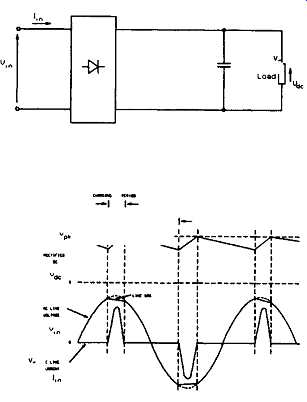
FIG. 1 Full wave bridge rectifier and waveforms (a) Circuit
(b) Waveforms
2 Definitions
2.1 Power Factor
The power factor is defined by: power factor = Real Power ! Total Apparent Power
= P / (V * I)
… where V and I are the total rms values of the input voltage and current, respectively.
The apparent power is expressed in volt-amperes, while the real power is expressed in watts.
2.2 Total Harmonic Distortion
A harmonic is a component of a periodic wave having a frequency that is an integral multiple of the fundamental power line frequency. For example, Fig. 2(a) shows a 50 Hz waveform and a 250Hz (50Hz x 5), 5th order harmonic of the fundamental frequency. Fig. 2(b) shows the corresponding waveform when the fundamental and the 5th order harmonic are combined. The resulting waveform which is not a sinusoid is a waveform with harmonic distortion. Harmonics are a steady state phenomenon, and should not be confused with the power transients which also distort the waveforms for a very small period of time.
The level of voltage or current harmonic distortion existing at any one point in a power system can be expressed as the Total Harmonic Distortion (THD) of the current or voltage waveform. The THD for a voltage waveform is given by the following formula:
! VrH D = (V: + V32 + ........ +VN2) ~ / V~
…where V 1 is the rms value of the fundamental voltage, and V n for n = 2, 3, 4, etc.
…are rms values of the respective harmonic voltages.
3 Harmonics and Power Factor
Harmonic distortions are usually caused by the use of nonlinear loads by the consumers of electricity. Nonlinear loads, a vast majority of which are loads with power electronic devices, draw current in a non sinusoidal manner, and with the increased use of such devices in consumer loads, the presence of distortions in current and voltage waveforms have become a frequent occurrence today.
For instance, virtually all modem computers incorporate an SMPS for converting mains AC voltage to DC voltages required by the computer circuits. The conventional SMPS is basically an AC-to-DC converter operating from a bulk storage capacitor which is recharged directly from the line through the input rectifiers. Since the rectifiers can only conduct when the line voltage is higher than the capacitor voltage, the charging of the capacitors takes place only during a small time period, resulting in narrow input current pulses as shown in Fig. 1(b).
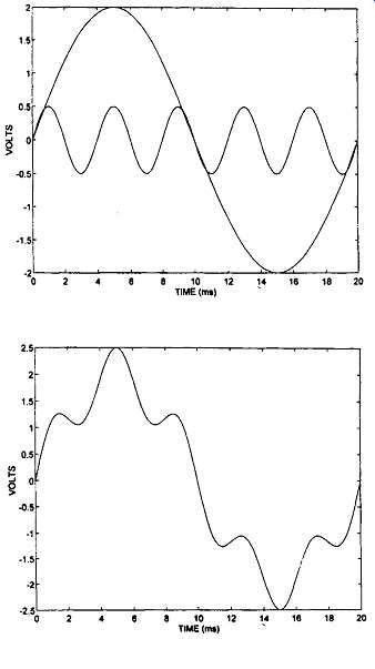 FIG. 2 Fundamental and the 5th order harmonic of waveforms
(a) Individual waveforms (b) Combined waveform.
Although the input current is nearly in phase with the voltage, the narrow pulses of the current have a peak value many times higher than would be present with a sinusoidal current waveform. The voltage waveform too is distorted, though much less than the current, with the peak flattened due to voltage drops caused by the high peak current flowing through the line impedance.
Only voltages and currents of the same frequency can produce non zero active power. Also, sometimes it may be reasonable to assume that the voltage is purely sinusoidal, despite the distortions in the current, and under such an assumption, V, the rms value of the voltage is equal to the rms of the fundamental frequency voltage V 1 and:
P ffi Vlltc°s t~l ffi Vltc°s ~l
Power factor =VItcos 01 / VI = Itcos 0t / I
= In phase fundamental rms current / Total rms current
An important observation that can be made here is that, even when the fundamental current is in phase with the voltage, i.e., cos (l)l = 1, the power factor can be less than one, since 11 is less than I when distortions are present in the current waveform. Conversely, as the harmonic content of the current approaches zero, the power factor approaches unity, provided there is no phase lead or lag.
The typical, non corrected, off-line power supply has a power factor between 0.6 and 0.7, a value that many suppliers and users have accepted in the past, believing that any attempt to improve it would add excessive cost to the power supply.
Adjustable Speed Drives (ASDs), Uninterruptible Power Supplies (UPS), electronic ballasts in energy saving lamps, and arc welders are some of the other common non-linear loads which draw current with harmonic distortion.
4 Problems Caused by Harmonics
Now let us look at the problems caused by these current harmonics to the rest of the utility system. To illustrate the problem due to current harmonics i h in input current i s of a power electronic load, consider the simple block diagram in Fig. 3.
Due to the non-zero internal impedance of the utility source L s (including the line connecting the source to the load), the voltage waveform at the point of common coupling to the other loads v will be:
[…]
Since i s contains harmonics i h, v the voltage at the point of common coupling is distorted, and thus the supply voltage to the other loads, which may cause them to malfunction.
On the other hand, the low value of load power factor due to the harmonics means larger currents drawn from the utility, or higher VA consumption, for a given real load (in watts). This increases the burden on the utility by overloading the system and consequent need for increased system capacity.
As an example, consider the power available to a DC load of a piece of equipment using two types of front end AC to DC conversions. The first uses a conventional rectifier and capacitive filter/storage element. The second uses a power factor corrected circuit.
On a conventional 15A, 120 V circuit, the continuous rms current must stay below 12A to comply with the UL limits for a 15 A circuit breaker. Accordingly, only 1440 VA are available. When the typical converter efficiency of about 75 percent and the power factor of 0.65 are considered, a conventional power supply can deliver only 702 W (1440 x 0.65 x 0.75) to the load. A power factor corrected front end, with an efficiency of 95 percent, can improve the power factor to 0.99, and, as a result, the power available to the load is 1015 W (1440 x 0.99 x 0.95 x 0.75). The extra power available is significant because of the ever-increasing power demands of today's computer equipment.
In addition to the issues discussed so far, some other problems caused by harmonic currents are: additional heating and possibly over-voltages due to resonance conditions in the utility's distribution and transmission equipment, errors in metering and malfunctioning of utility relays, interference with communication and control signals, and so on. Some consequences of harmonics include unexpected failure of motor drives and power supplies, and random tripping of circuit breakers.
Frequently harmonic distortion results in down time and productivity loss.
5 Harmonic Standards
In view of the widespread use of power electronic equipment connected to utility systems, various national and international agencies have proposed limits on harmonic current injection to the system by this equipment, to maintain good power quality. As a result, the following standards and guidelines have been established that specify limits on the magnitudes of harmonic currents and harmonic voltage distortion at various harmonic frequencies. (Power Quality Assurance Journal, September/October (1995) and Mohan, Undeland, and Robbins (1989)). (a) IEC Harmonic Standard 555-2, prepared by the International Electrotechnical Commission, and accepted by its National Committees of the following countries: Austria, Australia, Belgium, Canada, Egypt, Finland, France, Germany, Hungary, Ireland, Japan, Korea (Republic of), Netherlands, Norway, Poland, Romania, South Africa (Republic of), Switzerland, Turkey, and the United Kingdom.
(b) EN 60555-2, "The Limitation of Disturbances in Electricity Supply Networks caused by Domestic and Similar Appliances Equipped with Electronic Devices," European Norm prepared by Comite Europeen de Normalisation Electrotechnique, CENELEC. This in fact is an adoption of the IEC 555-2 standard to the CENELEC member countries, and will be same for all countries in the European Union.
(c) IEEE Standard 519-1992, "IEEE Recommended Practices and Requirements for Harmonic Control in Electrical Power Systems."
5.1 IEC 555-2
IEC 555-2 provides harmonic current limits for all electrical and electronic equipment having an input current up to 16 A, intended to be connected to public distribution systems of nominal 50 or 60 Hz frequency. The voltages covered are 220-240 V single phase, and 380-415 V three phase. The equipment is classified into four groups: "Class A, for balanced 3-phase equipment and anything else that does not fit into another group; Class B, for portable tools; Class C, for lighting equipment; and Class D, for equipment having an input current with a special waveshape." (IEC Standard Publication 555-2 1982).
The harmonic limits are defined in absolute values, irrespective of the equipment's power rating. Table 1 below gives the maximum permissible harmonic current in amperes in these four groups according to the IEC 555-2. The same limits are shown in a bar chart in Fig. 4.
TABLE 1 IEC 555-2 Harmonic Current Content Limits
Odd Harmonics Even Harmonics
Harmonic Order (n)
Maximum Permissible Harmonic Current (A)
6 Power Factor Correction
Power factor correction or control in these situations, where low value of power factor is a result of the presence of distortions in the current waveform, fundamentally means eliminating those distortions. In other words, the goal is to make input current look like input voltage on a moment-by-moment basis, the same as it would with a resistive load. Fig. 5 shows line voltage and line current with and without power factor correction.
In low power supplies, this can sometimes be accomplished by adding an inductor in front of the bulk capacitor. At high power levels, a more sophisticated passive component solution, such as a ferroresonant input transformer or tuned input filter may be possible. While these approaches may be able to improve power factor to greater than 0.9 in power systems, they all suffer from the growing bulk, weight, and cost as power levels increase. In addition, they are only effective over a limited range of operating voltages and power levels.
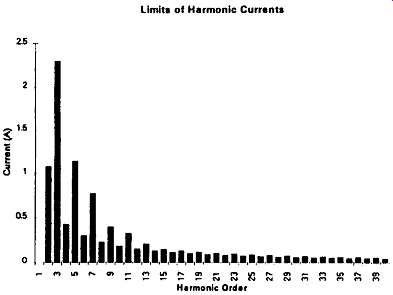
FIG. 4 Limits of harmonic current content according to
IEC 555-2 ---Limits of Harmonic Currents
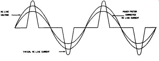
FIG. 5 Effect of power factor correction on line current
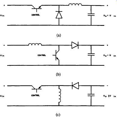
FIG. -6 Three basic converter topologies that can be
used for power factor correction (a) Buck converter (b) Boost converter
(c) Buck-boost converter
6.1 Active Power Factor Correction
Most designers now seem to agree that a more effective solution can be achieved with the active approach which incorporates a separate switch mode power converter con figured as a current-programming pre-regulator. While adding complexity to the power supply, this type of pre-regulator can be implemented to yield a higher power factor over a broader range of operating conditions with smaller size and less weight and power loss than any passive solution.
The essential difference between the power factor pre-regulator and the conventional switch-mode regulator is that the former restores the input current to a near-sinusoidal state, while the latter only deals with the regulation of the output voltage. Like the conventional regulator, the power factor regulator can use any one of the three basic converter topologies described in Section 3, namely: buck, boost, and buck-boost (fly-back). Each of these topologies ( Fig. 6) has distinctive characteristics.
The buck converter ( Fig. 6a), For example, has major limitations. In order to regulate the output, the output voltage of a buck converter must be less than its minimum input voltage. Because there is a break in the input current when the input voltage falls below the output voltage, the buck converter cannot provide optimal power factor correction. However, a buck converter may be satisfactory for low output voltage applications having moderate power factor requirements. The chopped current of the buck regulator, which can generate considerable line noise that is difficult to filter, is also a major concern. Another disadvantage is that the maximum input voltage appears across the switch, and its base (gate) drive usually requires level shifting to a floating reference. However, because the switch is at the input, the buck converter can control input surge current and also provide protection against an output overload or short circuit.
The buck-boost (fly-back) converter ( Fig. 6c) can either step down or step up the input voltage. Because of this, it offers the advantage of an independent choice of output voltage. Also, it’s simple to isolate the output (with an extra winding on the inductor), so that a single stage can accomplish power factor correction and isolation. In a circuit that is not transformer coupled, a buck-boost converter inverts the output polarity with respect to the input. Since in this topology there is no path to AC ground unless the switch is closed, the buck-boost converter can provide current limiting, during both steady state operation and initial turn-on.
One disadvantage of the buck-boost converter is that the switch has to withstand the sum of the input and output voltages. Also, the buck-boost converter operates in the discontinuous mode, which causes it to exhibit peak currents two to four times higher than the average line current. The noise created by this can be a serious problem. Because these high peak currents degrade efficiency too (especially at higher power levels), power factor correction circuits using this topology are limited to about 150W in practical applications. Fluorescent lamp ballasts and personal computer power supplies are typical applications.
Probably the most popular topology for a power factor pre-regulator is the boost converter ( Fig. 6b), which steps up the input voltage. Because the boost converter operating in the continuous mode does not chop the input current, and because the inductor itself acts as a line filter, RFI and EMI problems are generally reduced. Also, having the inductor in the input circuit makes it easy to implement current mode control.
Another advantage of the boost converter is its ability to maintain control over the complete input voltage waveform, thereby minimizing distortion, an important consideration in power factor control. In addition, the switch's common emitter configuration makes it easy to drive the base of the switch with ground referenced control signals. Moreover, the voltage across the switch is limited to the value of the output voltage. Because its peak current tends to be much less than that in other topologies, the boost converter is particularly effective for use in high power supplies. The major disadvantage of the boost converter is its inability to easily provide short circuit protection. Table 2 is a summary of the merits and demerits of the three active power factor correction converter topologies.
===
TABLE 2 Comparison of Converter Topologies with Power Factor Correction
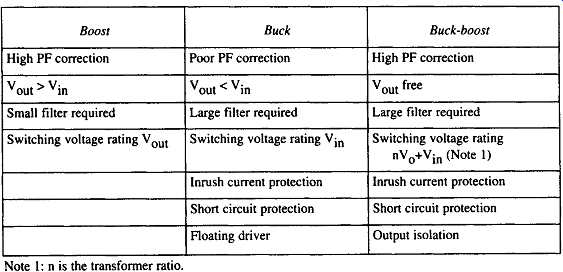
Boost Buck Buck-boost High PF correction Poor PF correction High PF correction Vout > Vin Vout < Vin Vout free Small filter required Large filter required Large filter required Switching voltage rating Vout Switching voltage rating Vin Switching voltage rating nVo+Vin (Note 1)
Inrush current protection Inrush current protection Short circuit protection Short circuit protection Floating driver Output isolation Note 1" n is the transformer ratio.
===
FIG. 7 Active current shaping (a) Boost converter (b) Line waveforms (c) Ivsl and i L
6.2 Implementation Using Boost Topology
The principle of operation of active power factor correction circuits is described here using the boost topology. The boost converter is generally preferred over buck or buck-boost converters for current shaping because in most applications, among other things, it’s desirable to stabilize the DC output voltage V o slightly in excess of the peak of the AC input voltage v s.
This converter is shown in Fig. 7(a) where C o is used to minimize the tipple in V o and to meet the energy storage requirement of the power electronic system. The DC current I_load represents the power supplied to the rest of the system and the high frequency component in the output current is effectively filtered out by C_o .
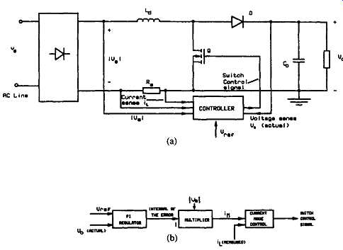
FIG. 8 Control of power factor correction circuit
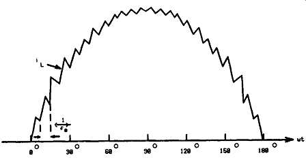
FIG. 9 Inductor current i L of the boost converter with
current mode control
The basic principle of operation is straightforward. At the utility input, the current i s is desired to be sinusoidal and in phase (~ = 0) with v s as shown in Fig. 7(b), so that the power factor (cos ~) is equal to 1. This means that, at the full bridge rectifier output in Fig. 7(a), its output current i L has to be of the same shape as the output voltage, which is the fullwave rectification of the supply voltage or Ivsl, as shown in Fig. 7(c). In other words, i L has to follow I v s !, so that i s will follow v s . However, i L is also the input current to the boost converter, and by operating the converter in the current regulated mode, i L can be shaped according to the supply voltage v s as desired. The feedback control is shown in a block diagram in Fig. 8(a). First, the output voltage V o of the converter is sensed and it’s compared with the desired output voltage Vre f. The difference is fed to a PI regulator, the output of which is the error signal to the multiplier ( Fig. 8(b)). Then i M, the desired value of the current i L is obtained by the multiplication of this error signal with the desired shape I v s I, and therefore, i M has the same shape as lv s I. The status of the switch in the boost converter is now controlled by comparing the actual current i L with the desired current i M. Once i L and i M are available, there are various ways to implement the current mode control of the boost converter, as discussed in Section 3. Among them, the fixed frequency pulse width modulation (PWM) is the most widely used technique.
Thus, the switching frequency fs is kept constant. When i L reaches i M, the switch in the boost converter is turned OFF. The switch is turned ON by a clock at a fixed frequency fs, which results in i L as shown in Fig. 9. As can be seen, the average value of i L has the desired shape which is I v s I.
6.2.1 Output Capacitor and Boost Inductor
The parameters that affect the choice of the output capacitance C o , which is used to minimize the tipple in V o and to meet the energy storage requirement of the power electronic system, are:
(a) Hold-up time capability, usually 20 ms for computer power supplies.
(b) Ripple current handling capability.
(c) Allowable third harmonic distortion.
Its value can be calculated using the formula,
Co 2Pot., a / (V2 min^2 --- Vo, .oi.)
…where, C o = output capacitance, Po = output power of the converter, thl d = hold-up time, normally 20 ms, Vo, min = minimum value of the output regulated voltage, and VoL, min
= minimum input voltage of the driven load, usually a switching power supply.
The value of the boost inductor affects many other design parameters. Most of the current that flows through this inductor is at low frequency. This is particularly true at the lowest input voltage where the input current is the highest.
Normally the acceptable level of ripple current is between 10 and 20 percent.
For a switching frequency of 100 kHz, the following formula will produce acceptable results.
L a = 300 / Po mH
A good detailed description of the calculation procedure can be found in Micro Linear Application Hand book.
6.3 Implementation Using Buck-Boost Topology
Unlike the boost topology, typical buck-boost topology implementation does not require a multiplier. This makes the buck-boost implementation much simpler, but it can be used only in low power applications, typically abut 150 W or below.
In a typical application, the buck-boost regulator operates in the discontinuous inductor current conduction mode. The inductor energy stored during the "ON" time of the switch is completely delivered to the output capacitance during the "OFF" time ( Fig. -6c).
At the beginning of each "ON" time the inductor current starts to ramp up from zero to a value that is proportional to the instantaneous value of the supply voltage as shown in Fig. 10.
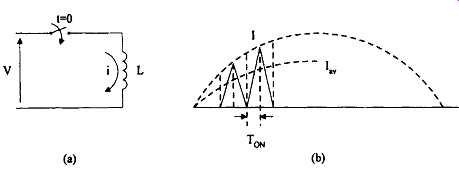
FIG. 10 Principle of the buck-boost topology used in
power factor correction
The instantaneous voltage: v_ Ld_~ i dt di v dt L
Assume the voltage v is constant and equal to av, during the small "ON" time period of the switch T_ON. Thus the current will reach a maximum value I according to the equation:
Thus the current at the end of each "ON" time is proportional to the instantaneous voltage at that time, and the average current Iav is a sinusoid as shown in Fig. 10b.
6.4 Multi-Stage Off-Line Converter
The obvious and most commonly used solution for providing PFC in a real- world system which requires both isolation and lower output voltage levels is a two- stage converter topology as shown in Fig. 11. While this configuration could be implemented in many different forms and with many different control elements, what has been shown here is the most basic approach which would be applicable to medium or lower power levels where a single-ended forward topology would be appropriate for the down converter. By providing separate controls for the PFC and buck stages, mixing and matching can be done to optimize the designs for each stage to meet performance and cost goals for a specific application. A two-stage converter will use a boost circuit for PFC followed by a buck stage to lower the output voltage and incorporate line isolation.
7 Power Factor Correction ICs
Active power factor correction requires special control circuits that are able to force the input current waveshape to be sinusoidal and in phase with the input sinusoidal voltage, as explained in the previous section. Traditionally, a decision to incorporate an active high power factor pre-regulator would not be taken lightly, particularly at high power levels, because of the complexity of circuitry required.
However, recognizing the existing and impending needs to provide a practical solution to the problem of active power factor correction, several vendors of integrated circuits have introduced devices specifically dedicated to the task. Among these vendors are Unitrode, Micro Linear, Motorola, Samsung, Cherry Semiconductor, and Silicon General.

FIG. 11 Two stage converter --- RECTIFIED AC LINE
7.1 UC3854
Unitrode's UC3854 is used in a boost topology and the chip includes a voltage amplifier, a low-offset analog multiplier, a current amplifier, a fixed frequency PWM, an oscillator, and a 1A totem-pole MOSFET gate driver. Also included is an enable comparator, and an over-current comparator, in addition to the 7.5V voltage reference. The greatly simplified circuit in Fig. 12 illustrates the basic operation of UC3854.
As shown, the circuit uses a current loop as well as a voltage loop for control.
The current loop samples the output waveform of the bridge rectifier through resistor R 7, which converts the voltage to a current waveform at pin 6 of UC3854. This input acts as a reference for the multiplier. To implement feed-forward line regulation, resistors R6, R 8 and R 9, together with capacitors C 3 and C 4, develop a DC voltage at pin 8 that is proportional to the rms value of the line voltage.
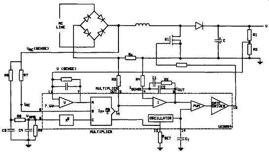
FIG. 12 Power factor correction circuit using UC3854
(Unitrode Inc., USA)
The chip squares this DC voltage and applies it to the multiplier. To complete the voltage loop, resistors R l and R 2 provide a sample of the output voltage V o and apply it to the input of the voltage amplifier at pin 11. The output of the voltage amplifier goes to the multiplier.
The output of the multiplier is a current that is equal to the product of the voltage amplifier output and the input line voltage (Ivsl), divided by the square of the rms line voltage (I M = AB/C). Acting as a control signal to the pre-regulator, I M has an instantaneous value that follows the shape of the input voltage, and an average value that is inversely proportional to its rms value. Resistor R 3 converts I M to a voltage while a voltage proportional to the line current is measured across R s, the line current sensing resistor.
The difference between these two voltages is applied to the input of the current amplifier. Under closed loop control, the current amplifier will try to keep this voltage difference close to zero volts. This forces the voltage produced by the return current on R s to be equal to the voltage across R3.
The amplified current error signal is then applied to the inverting input of the PWM comparator. The other input of the PWM comparator is the ramp generated by the timing capacitor C T of the oscillator. Pulse width modulation is obtained when the amplified error signal that sets up the trip point modulates up and down.
The output of the PWM is connected to a totem pole driver capable of sourcing and sinking +_1 A peak. As shown in Fig. 12 the PWM and the gate driver control the ON-OFF action of the MOSFET power switch S l to force the input line current to follow the programmed value. The UC3854 uses average current control; the compensation network comprising R4, R 5, C1, and C 2 performs the averaging.
R_SET programs the charging current of the oscillator and the maximum output of the multiplier. C T sets the PWM oscillator frequency.
The maximum output voltage level is internally limited to 18V, while the under-off voltage lockout comparator incorporated with the output will turn the circuit off before the PWM output drops below 8V. Since the chip uses average current control, it can accurately maintain sinusoidal line current without resorting to slope compensation. UC3854 provides power factors to 0.99, and limits the line current distortion to less than 5 percent. The chip operates in systems with line voltages of 75 to 275 V and line frequencies of 50 to 400 Hz. When compared with other power factor controllers, the UC3854's higher reference voltage (7.5V) and higher oscillator output (5V) can offer advantages in high-power supplies, which typically exhibit high noise.
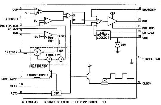
FIG. 13 Functional block diagram of ML4812 (Micro Linear
Corp., USA)
7.2 ML Series of ICs
Micro Linear Corporation offers several power factor correction ICs. Among them, ML4812 is designed to optimally facilitate a boost type power factor correction system. Special care has been taken in the design of the ML4812 to increase system noise immunity. The circuit includes a precision reference voltage, oscillator, multiplier, error amplifier, over-voltage protection, ramp compensation as well as high current output. In addition, start-up is simplified by an under-voltage lockout circuit with 6V hysteresis. A block diagram of ML4812 showing the basic building blocks is given in Fig. 13.
The operation of the circuit is similar to that of UC3854, as explained before.
A fraction of the output voltage is fed to the error amplifier through pin 4. A current that is proportional to the input full-wave rectified voltage is fed to the pin 6. The output of the multiplier is applied to a resistor in the external circuit through pin 2.
The difference between the voltage produced by this and a voltage proportional to the line current which is fed to pin 1, is applied to the PWM comparator which in turn controls the switch.
In a typical application, the ML4812 functions as a current mode regulator.
The current which is necessary to terminate the cycle is a product of the sinusoidal line voltage times the output of the error amplifier which is regulating the output DC voltage. Ramp compensation is programmable with an external resistor to provide stable operation when the duty cycle exceeds 50 percent. The use of ML4812 in a continuous mode boost circuit using current mode control scheme is shown in Fig. 14 with the resulting current waveforms. Typical applications include computer systems that require optimum power factor correction.
ML4813 is designed to optimally facilitate a discontinuous buck-boost type power factor correction system for low power, low cost applications. A functional block diagram of ML4813 is shown in Fig. 15. Similar to ML4812, this too has a precision reference voltage, oscillator, error amplifier, high current output, and an over-voltage comparator, and special care has been taken in the design to reject system noise. This too has an under-voltage lockout circuit with 6V hysteresis.
However, unlike ML4812, ML4813 does not have a multiplier and there is no multiplication of the error amplifier output with the input fullwave rectified voltage Ivsl. Instead, in ML4813, "ON" time of the switch is set by the error amplifier and the PWM comparator according to the instantaneous value of Ivsl, a portion of which in this case is the external input to the error amplifier.
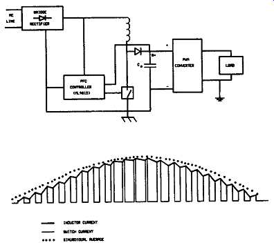
FIG. -14 Boost mode power factor correction using ML4812
and inductor current waveform (Micro Linear Corp., USA) (a) Block diagram
(b) Waveforms
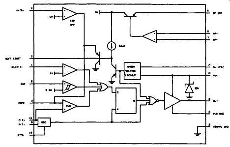
FIG. -15 Functional block diagram of ML4813 (Micro Linear
Corp., USA)
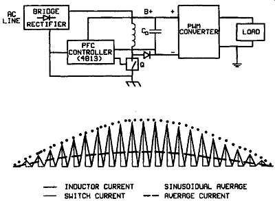
FIG. 16 Buck-boost power factor correction using ML4813
and inductor current waveform (Micro Linear Corp., USA) (a) Block diagram
(b) Waveforms --- .---- CONTROLLER; INDUCTOR CURRENT SINUSOID; SWITCH CURRENT
----- CURRENT
In a typical application, the ML4813 functions as a voltage mode, discontinuous current, buck-boost power factor regulator as shown in Fig. 16. The regulator operates in the discontinuous inductor current conduction mode. The inductor energy stored during the "ON" time of the power switch Q is completely delivered to the output capacitance during the "OFF" time. At steady state conditions, the inductor current at the beginning of the "ON" time starts to ramp up from 0 Amps to a value that is determined by the instantaneous value of the input full wave rectified voltage; the "ON" time as it’s set by the error amplifier and the PWM comparator; and finally by the inductor itself.
By maintaining a constant duty cycle, the current follows the input voltage, making the impedance of the entire circuit appear purely resistive. With the buck- boost circuit, power factors of 0.99 are easily achievable with a small output inductor and a minimum of external components.
The discontinuous mode, buck-boost topology used in MLA813 is particularly well suited for low power applications such as fluorescent ballasts and low power switching supplies. Also, it’s a useful topology when there is a requirement for the output voltage to be lower than the peak input voltage, or where an isolated output is required. This is not possible with the boost topology, where the output voltage must always be higher than the maximum peak of the input voltage range. The typical input range for the buck-boost power factor regulator is from 90 VAC to 260 VAC. A comparison of the two circuits based on ML4812 and ML4813 is given in Table 3.
===
TABLE 3: Comparison of the two power factor correction circuits in Figs 14 and 16.
Continuous, Boost
Output Voltage Vout > Vin Input Current Continuous Output Current Discontinuous Control Simple Current Mode Peak, Current (150 W) 2A Transformer Isolation Not Possible Rectifier Needs Fast V_max on power, Switch Vout Surge Current Limit Difficult Input Transient Absorption Inherent Input Line Filter Minimal Usable Power Levels 75 W to Over 2000 W Controller ML4812 Discontinuous, Buck-Boost Independent of Vin Discontinuous; Discontinuous Simple Voltage Mode 9A Easy Moderate V_out + Vin (peak)
Inherent Not inherent Complex x network, Below 150 W dL4813
===
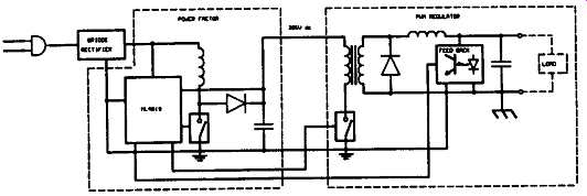
FIG. -17 Combined PWM and power factor controller in
ML4819 (Micro Linear Corp. USA)
The third IC offered by Micro Linear is the ML4819, which combines a boost- mode power factor circuit similar to the ML4812 with a conventional PWM controller circuit. The PWM section can be used for either current or voltage-mode control for a second-stage converter. Fig. 17 is a simplified diagram of the individual functions. Combining the two circuits in a single device minimizes the component count and saves space. Because both circuits share the same oscillator, synchronization is inherent. Moreover, a large oscillator amplitude of 4.3 V maximizes noise immunity.
The power factor section uses peak current sensing, and the programmable slope compensation is common to both sections. The PWM section includes cycle-by-cycle current limiting as well as duty cycle limiting (for single-ended converters). Both sections feature individual 1A totem-pole output driver but the under-voltage lockout function is shared.
In addition, Micro Linear offers MLA821, the operation of which is similar to MLA812 but for power ranges above 500 W. Also, Micro Linear offers ML4824, the operation of which is similar to ML4819 but for power ranges above 1000 W. 9.7.3 MC34262, MC33262
Motorola's MC34262 and MC33262 are high performance, critical conduction, current mode power factor controllers specifically designed for use in off-line active pre-converters. These devices provide the necessary features required to enhance poor power factor loads by keeping the AC line current sinusoidal and in phase with the line voltage.
The two chips contain many building blocks and protection features employed in modem high performance current mode power supply controllers, as shown in Fig. 18. However, unlike the previously described chips, these devices don’t contain an oscillator.
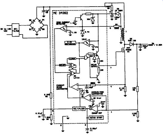
FIG. 18 Power factor correction circuit using MC34262
(Motorola)
These devices contain an error amplifier with access to the inverting input and output. The amplifier is a transconductance type. It has high output impedance with controlled voltage to current gain. The output of the error amplifier connects internally to the multiplier, with pin 2 available for external loop compensation. The error amplifier monitors the average output voltage of the converter over several line cycles, resulting in a fixed drive output on time.
Another key feature in using a transconductance amplifier is that the input can move independently with respect to the output, because the compensation capacitor connects to ground. This allows dual usage of the voltage feedback input pin by the error amplifier and the over-voltage comparator.
The MC34262 operates as a critical conduction current mode controller, whereby the zero current detector initiates output switch conduction. Switch conduction ends when the peak inductor current reaches the threshold level established by the multiplier output. The zero current detector initiates the next ON time by setting the RS latch at the instant the inductor current reaches zero. This critical conduction mode of operation has two significant benefits.
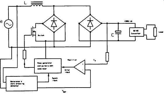
FIG. 19 Active low frequency power factor correction
circuit (Unipower Corp., USA)
First, because the MOSFET cannot turn on until the inductor current reaches zero, output rectifier reverse recovery time is less critical, allowing use of an inexpensive rectifier. Second, there are no dead time gaps between cycles, so the AC line current is continuous, thus limiting the peak switch to twice the average input current. The under-voltage lockout comparator in the chip guarantees that the IC is fully functional before enabling the output stage (Alberkrack and Barrow 1993).
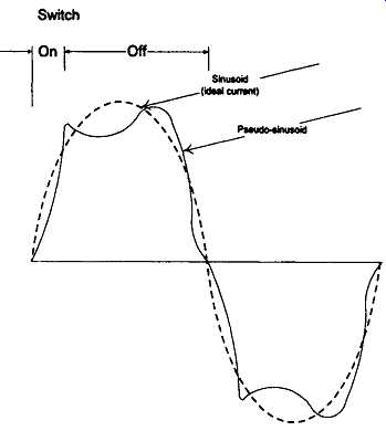
FIG. 20 Pseudo-sinusoidal input current produced by active
low frequency power factor correction
8 Active Low Frequency Power Factor Correction
All of the circuits we have discussed so far were active high frequency power factor correction circuits which typically operate at switching frequencies of 20 kHz to 100 kHz, far higher than the line frequency.
Active low-frequency (LF) PFC circuits operate at a switching frequency of twice the line frequency, 100 or 120 Hz, and in synchronism with it. This method uses an active switch, a LF inductor, and a control circuit to perform PFC. One way to implement active-LF correction is through a patented technique used by Unipower Corp. ( Fig. 19). This circuit was chosen because of its simplicity and because it provides the best overall performance with minimum impact on size, efficiency, reliability, EMI, and cost.
The MOSFET-switch circuit is driven into conduction at the zero crossing of the AC-source voltage, and current builds up in the inductor, L, from the AC source.
At a controlled time after the zero crossing (typically 1 to 2 ms), the switch is turned off and the source current through L transfers to the output rectifier and filter circuit. The MOSFET switch is driven by a pulse-width-modulation (PWM) circuit that compares an error-feedback signal to a ramp signal that is synchronized by a zero-crossing signal.
The reference for the error amplifier is proportional to the rms value of the AC-line voltage, and the output voltage (about 300 V DC) is load-regulated by adjusting the conduction time of the MOSFET switch. The input-current waveform is enhanced by maintaining an optimum relationship between the magnitude of the AC-input voltage and the DC-output voltage.
The result is a pseudo-sinusoidal current waveform which gives a high power factor of 0.96 to 0.98 with low harmonic currents ( Fig. 20). Power factor at rated load is relatively constant over line voltage ranges of 90 to 132 V AC or 180 to 264 V AC. These input ranges can be made switch-selectable, or autoranging techniques can be used to provide automatic switching.
This method is highly efficient, with lower total losses than the HF method.
Its low component count also results in high MTBE A summary of the advantages and disadvantages of the active LF method is given in Table 4 (Hunter 1992).
===
TABLE 4 Active Low-Frequency Power-Factor Correction
Advantages | Disadvantages
• High efficiency • Hold-up time changes with line voltage
• Simple circuitry • DC bus not regulated
• High MTBF • Larger and heavier than high frequency method
• High PF (0.96-0.98)
• Low EMI
• Low harmonic distortion
• Wide frequency range
• Lowest cost
• Moderate input-voltage range (90 to 132V AC or 180 to 264V AC)
===
9 Evaluation of Power Factor Correction Circuits
Input power factor, harmonic current content, and waveshape are all used when describing the performance of a power factor correction circuit. To measure power factor, one must have a very reliable power meter that accurately measures both apparent power and true average power. Some of the older model meters that measure power factor by determining the phase angle between the current and voltage waveforms won’t serve our purpose.
The true average power for distorted AC waveforms can only be determined when the current and the voltage are simultaneously sampled, then multiplied and integrated. One should be very careful about which meters are trustworthy when it comes to measuring power with non-sinusoidal and noisy waveforms.
Harmonic current content also has to be measured using a similar meter or using a spectrum analyzer. The IEC 555-2 standard requires current content conformity to the 40th harmonic.
Efficiency of the power factor correction circuit also is an important indicator of the performance of the circuit. Efficiency measurements require accurate measurement of the output average power as well as the input average power. Because the output voltage as well as the output current is DC, one might just use something like a lab bench top meter to measure the two readings. However, in order to get truly accurate efficiency measurements, the same power meter should be used to measure both the output as well as the input power.
