AMAZON multi-meters discounts AMAZON oscilloscope discounts
..
- Introduction
- Evolution of Power Integrated Circuits
- BCD Technology
- Applications of Power Integrated Circuits
- Power Hybrids
- Smart Power Devices
- Smart Power Microcontrollers
- System Components and Impact of IGBTs
- Future
1 Introduction
From their humble beginnings as audio amplifiers, Power Integrated Circuits (PIC) are now moving towards a more prominent role in many power electronic systems. Today an increasing number of applications make use of these devices.
Usually power integrated circuits are designed for specialized applications in the lower power range. Their concept represents the natural continuation of IC evolution, realizing a complete system on one chip.
The power limit arises from the amount of heat that can be dissipated by a silicon surface of approximately one square centimeter in size. When most of the silicon real estate is devoted to power devices the chips are usually called "smart power." However, the terminology applied is more often based upon institutional rather than technical reasons.
What constitutes a power integrated circuit varies from manufacturer to manufacturer, depending on their product portfolios and point of view; that is, whether they approach the market from a discrete-transistor or an IC perspective. Some define power ICs by their functions--whether the IC actually includes the power transistor itself, others, by the IC's voltage and current levels, and still others by the IC's general involvement in controlling power.
Smart power is cost-effective today in many applications because additional functions can be combined on the chip at low cost, which would be expensive or impractical to add using discrete components. These functions include drive circuitry, thermal protection, over and under voltage protection, current limiting, and diagnostics. Many smart power products were originally developed to meet the demanding environmental and cost constraints of the automotive and consumer electronics industries. As a result, industrial applications, where numbers produced are lower, also have made use of these devices in the recent past. The technology is steadily progressing towards much more complex devices such as Smart Power Hybrids, Smart Power ICs, Smart Power Microcontrollers, etc., all of which could be generally grouped as Intelligent Power Modules (IPM).
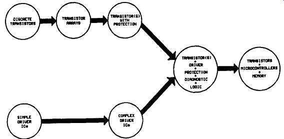
FIG. 1 Progress of power integrated circuits
2 Evolution of Power Integrated Circuits
Fig. 1 indicates how two independent paths starting from discrete transistors and simple stand alone driver ICs have progressed independently towards the levels of integration in power ICs available in the mid 90s. The figure shows two independent paths of devices, beginning with discrete power transistors and driver ICs. As integration increases, each device adds functions until the transistors and driver combine into one.
With the advent of process technologies that can integrate virtually everything but the load itself, the current capabilities of ICs for power actuation and switching seem almost limitless. The potentially integrated functions include logic and control, sometimes implemented by a fully functional microcontroller; protection; diagnostic feedback; and, finally, a power output stage. Whether you call it "smart" or "intelligent" power, the technical feasibility of combining these functions into one IC using some mixture of bipolar, CMOS, and Double-Diffused MOS (DMOS) structures is proven. The process titled BCD (bipolar, CMOS, and DMOS) or its variations are used by most component manufacturers.
In the discussion of the development of PICs, it’s quite clear that drivers and discrete power transistors can produce the most flexible designs. Two developments contribute to this flexibility: the wide availability of discrete transistors, particularly power MOSFETs, and the increasing numbers and types of drivers, particularly MOSFET drivers.
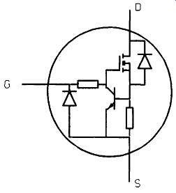
FIG. 2 Current limiting MOSFET
Regardless of the driver you select, you can independently select a MOSFET based on the design's speed and efficiency. Vendors of these MOSFETs also continue to make dramatic improvements in the device's efficiency. The on-resistance (rDS(ON)) of state of the art TO 220 packaged N channel MOSFETs may be around 10mf] at 60V. A similarly packaged, state of the art P channel device has an on- resistance of around 45mf~. Integrated power transistors just cannot compete with discrete transistors on the basis of rDS(ON) alone. There is a trade-off between specific on-impedance (a measure of rDS(ON) versus die area) of discrete transistors and ICs. Most power ICs have higher specific on-impedances than do discrete devices, simply because of fabrication differences that result in the ICs' larger power structures. An IC requires two to four times more die area than does a discrete transistor to achieve the same on resistance; such a large die area makes ICs too expensive to produce. The on resistance values also depend on vendors' proprietary processes and voltages.
Use of discrete transistors also provides two other advantages: reduced size and increased protection. Discrete transistors are undergoing a dramatic shrinkage.
Manufacturers of discrete transistors have also found inexpensive ways to add protection features, such as overcurrent protection and output-voltage clamps. In newer families such as "intelligent discretes" small transistors, diodes, and resistors etc. are added to provide intelligent device control.
These control devices can be as simple as one bipolar transistor and two resistors. Since they are fabricated within the standard power MOSFET process and generally take up a very small silicon area, the cost that they add to the base device is minimal. This is more than offset by the added value these control elements provide.
FIG. 2 indicates a very basic representative device from such a family from Harris Semiconductors Inc., which is categorized as a current limiting power MOS- FET. The idea of these types of devices is to provide the designers with the basic terminal configuration (drain, source, and gate) externally, but the internal device carries many more added features to the device.
In today's component market, many types of drivers are available, particularly for driving MOSFETS and IGBTS. The term "MOSFET driver" refers to a wide range of devices. They all provide a buffer between the analog control circuitry and the true power world. These drivers suit a wide range of applications, including motor controls, power supplies, UPS systems, automobile braking systems, air bag deployment, and industrial controls.
Although these drivers lack a power transistor, they can still implement protection. A separate driver can sense over current with suitable feedback. Some drivers can also sense insufficient gate drive voltage ma form of under voltage protection to prevent the MOSFET from operating in its potentially destructive linear region.
Integrated power and driver ICs can do things that drivers and discrete transistors often cannot. For example, ICs that integrate the driver and power transistor or transistors can boast about all the protection features of discrete transistors, including thermal protection, which discrete transistors cannot easily implement.
ICs in particular can add thermal protection without additional components.
Combining power devices with a microcontroller and memory currently represents the highest level of integration. To date, a number of manufacturers, including Motorola, Phillips, SGS Thomson, and Texas Instruments, have demonstrated this capability (Kerridge 1994). In 1990, Motorola integrated its 8-bit 68HC05 core with 96 bytes of RAM and 2064 bytes of user ROM and 240 bytes of ROM for test functions.
More recently, SGS Thomson unveiled its third-generation BCD3 process with which the company can combine an ST6 8-bit microcontroller with a DMOS H- bridge power stage, driver and interface functions, a charge pump, and thermal protection. Using BCD3, the company can also integrate EEPROM, making the IC configurable by hardware and software. These programmable power devices or power PLDs contradict the notion that "high integration means narrow application."
3 BCD Technology
First introduced in 1986, mixed Bipolar-CMOS-DMOS (BCD) smart power technology has brought significant advances in the art of integrating signal and power circuits on the same chip. IC technologies combining power DMOS with signal circuits had existed previously, but BCD technology differs by the use of isolated DMOS power transistors having all of the contacts on the top surface. In contrast, other processes used discrete-type DMOS structures where the lower surface of the die is the drain contact, so that two or more DMOS devices can only be placed on the same chip if they have a common drain contact.
With the advent of BCD technology, designers were free for the first time to integrate as many DMOS power transistors as they wished, and to interconnect them in any way. Thus it became feasible to produce smart power ICs with half-bridge and bridge output stages, and even integrate several output stages on the same chip.
The first commercial circuits to be produced with this technology were H-bridge motor driver ICs (operating on supply voltages of 48V and delivering 1.5 A continuous output current) and SMPS ICs capable of delivering 10A output current.
In the early 1990s the original four micron BCD technology was superseded by a shrink 2.5 micron version, bringing a doubling of both signal circuit density and current density in the power section. With the introduction of this second generation version (BCD2), designers were no longer restricted by die size concerns and quickly learned to make increasingly complex ICs. Another important trend was to develop high voltage technologies. A 250V evolution of BCD technology has been developed for applications in the industrial and telecom fields.
In the 3rd generation of BCD technology (BCD3) the lithography is reduced to 1.2 Ixm. Apart from the increased density, this evolution allowed the convergence of technologies too. This 1.2 lxm BCD technology is compatible with the existing 1.2 l.tm CMOS technologies (SGS Thomson Microelectronics, 1994). CMOS transistor packing density is 5000 transistor/mm^2, three times greater than the previous generation technology. The DMOS power transistors also take up less space, due to their low resistance of 0.25 D./mm^2, which is half that of BCD2.
Other improvements over BCD2 include double polysilicon layers and double level, triple thickness metal layers, which help achieve the high levels of integration. The signal section density reaches a level where it’s economically feasible to integrate an 8-bit microcomputer core and peripheral circuits on a smart power chip. EEPROM or EPROM memory can be added, too.
4 Applications 'of Power Integrated Circuits
To justify the distribution of non-recurrent engineering costs (involved in the development of PICs) among a large number of components, PICs are currently used in special market segments such as:
(a) Automotive applications (b) Disk-drives (c) PWM systems for bidirectional stepper and DC motors (d) Electronic ballasts for fluorescent lighting (e) Off-the-line switchmode power supplies (f) Special classes of power amplifiers
Typical auto applications include control of mirrors, seats, windows, and instrument panels, and all require ICs with approximately 60V, 4A rating. Many of these specialized products, particularly automotive ones, have spilled over into the general industrial market, starting out as custom ICs and eventually becoming standard offerings.
Although it seems that most highly integrated power ICs are geared toward the automotive industry, vendors do develop many ICsm specialized motor controllers and drivers, in particular for many computer peripherals and industrial applications. Some of these drivers now integrate PWM to drive bidirectional stepper and DC motors. One example is Allegro Microsystems UDN 2961B/W half bridge with 45V and 3.4A ratings. This power IC is usable in printer hammer or motor driver applications.
Although the automotive and disk drive markets are huge, numerous other products target the more fragmented industrial markets. Also, emerging high volume markets are pushing the development of power ICs with high voltage and current requirements. The foremost example is the integration of high-voltage structures generally greater than 100V with logic-level circuitry. Over 20 semiconductor companies worldwide, including AT&T Micro-electronics, Harris Semiconductor, International Rectifier, Power Integrations, and SGS Thomson, are pursuing high-voltage control applications. One of the high-volume markets driving much of this work is the electronic ballast for fluorescent lighting.
Applying IC technology to electronic ballasts is hot for two reasons: a worldwide drive for energy efficiency is causing a boom in the fluorescent-lighting industry, and real money, in the form of utility-company subsidies to consumers, is behind the increased-efficient-energy effort. On the technical side, high-voltage IC technology has progressed to the point at which vendors can build low-cost ICs that can compete with existing electronic ballast designs. Older designs typically use a pulse transformer and discrete transistors.
Using an IC eliminates the need for a transformer, thus easing the design, increasing efficiency, and reducing the design's size. A recent example of a low-cost approach for this application is International Rectifier's IR 2155 IC for energy saving lamps.
5 Power Hybrids
Power hybrid ICs are available in a variety of circuit configurations, power capabilities, and packaging styles. Examples of available circuits include solid-state relays and circuit breakers, half-bridge and full-bridge drivers, 3-phase drivers, and DC/DC converters. See Table 1 for a representative list of power hybrid ICs.
Because of their specialized construction, hybrid ICs are often more expensive than equivalent combinations of monolithic ICs and discrete power devices. This higher cost is particularly true for military-grade hybrid ICs, which make up a large part of the market. Despite the cost, hybrid ICs have the redeeming characteristics of small size and the ability to combine specialized circuitry in a single package.
A key factor in obtaining these characteristics is the extensive use of chip- level and surface-mount components, including both active and passive types.
Typically mounted on an alumina or beryllia substrate, such components minimize the size of the final package and allow flexibility in the design of the overall circuit.
A power hybrid can be as simple as a half-bridge driver or as complex as a DC/DC converter that contains all of the necessary active and passive devices, including magnetic components and filtering elements. Highly specialized hybrids often contain dozens of components and can be quite elaborate.
Another common circuit block implemented in power hybrid technology is the operational amplifiers for high voltage and high current applications. For example, PA89 ( Fig. 3) power operational amplifier from Apex Microtechnologies Inc. is capable of providing 75mA of continuous output current while operating over a supply range of ±75 to ±600V. The op amp is designed for use in specialized applications such as piezoelectric drives, high-voltage instrumentation, and electrostatic deflection. With its output-bridge configuration, the op amp could provide a 1000V p-p output signal with programmable current limiting.
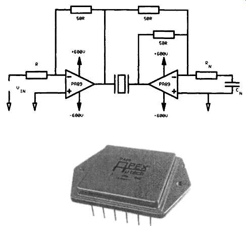
FIG. 3 A power operational amplifier in hybrid form used
for a piezo drive (Apex Microtechnologies Inc., USA) (a) Implementation (b)
Photograph
For applications where a standard hybrid circuits are unable to provide customer requirements, several companies supply custom circuits. Phillips Circuit Assemblies, For example, has a number of technology choices from which they can fabricate application-specific circuits. Such companies work directly from the user's schematic and convert it to a hybrid circuit that saves space and usually has superior environmental ruggedness and greater reliability than conventional approaches. Hybrid modules with IGBTs are discussed in section 10.7.
===
TABLE 1 Some Representative Power Hybrid Circuits
Company Apex ~t-Tech Gentron ILC Data Device Modupower Motorola Omnirel SGs-Thomson SIPEX Part No. PA03 SSR Series GS-105 PWR-82331 SSP-21110 Mp7000 Series MPM3002 MPM3003 OMg011SF GS-R400V SP2805 Circuit Type Power Op Amp Solid-State Relays Half-Bridge Motor Driver 3-Phase Bridge Motor Driver Solid-State Power Controller Buck Regulators MOSFET Half- Bridge MOSFET 3- Phase Bridge Circuit Power Module Step-Down Switching Regulator Converter Max Ratings 75V, 30 A 1200V, 25-125A 400V, 25A 200V, 30A 28V, 2-25A 15V, 1A 00v, 8A 60V, 10A 100V, 18A 5 to 40V, 4A 5V, 10A Features 1 mhz Gain-Bandwidth Product, 30 KHZ Power Bandwidth, 8v/I.tsec Slew Rate.
Uses MOSFET or IGBT Switches Simultaneous-Conduction Lockout, Over Current Protection, Isolated Package.
Mil-Std-883C, Six MOSFETS, Six Diodes, Digital Control, and Protection Circuitry Contains High-Side MOSFET Switch, Driver, and Isolated Controller , Combines 5-Terminal Regulator with Magnetic and Filtering Elements Icepak Power Modules for Single and 3-Phase Motor Drive. Used With Company's MCxxxx Series Of Control ICs Mtl-Std-883C Process, Four MOSFETs, Four Rectifiers, and Four Schottky Diodes ,, Programmable Output Voltage, Soft- Start, Short-Circuit, and Thermal Protection 1MHZ Operation, Has Input/Output Filters, Transformer, Switching Transistor, and Control
....
===
6 Smart Power Devices
The term "smart power" is difficult to define. Because of its catchy name, vendors have applied the term to products that only marginally qualify as smart- power devices. Some definitions specify an output voltage rating of 50V or greater without regard to the device's current rating. Any reasonable definition of smart- power specifies a power-handling capability of at least 1W. Far more difficult to define than a minimum power rating is the amount of intelligence or "smarts" a device needs to qualify as being smart. The intelligence can be in the form of control functions, interface capability, or fault management.
The basic idea underlying smart power technologies is to modify MOSFET or bipolar transistor technology to create islands for digital and analog signal processing functions. If possible, the signal section ICs should not reduce the performance of the power section.
Despite the lack of a commonly accepted definition, smart-power ICs represent a technology that is applicable to many of today's system requirements. These intelligent circuits ease the interfacing of digital and analog ICs with discrete power devices. With most of the required circuitry contained in a single package, both monolithic and hybrid smart-power ICs offer system designers the benefits of reduced size, greater reliability, and protection. This last benefit is often where a smart-power device really demonstrates superior intelligence by protecting itself against potential catastrophes such as voltage over-loads, short circuits, and thermal runaway.
When designing a smart-power integrated circuit, several issues that are not of great importance in standard low-power designs need be addressed. Among the most important issues are current, voltage, and safe operating area of the power transistors in the IC. Other considerations are proper layout, length, and width of the high-current interconnect lines. Also important is the proper design of the intermediate or drive stages for the power transistors and the effects of heat generated in the power transistors on the small signal circuitry in addition to proper design and layout of the circuitry. The proper choice of parallel and series connections of resistors with respect to their ohmic value and power requirements is also important. Finally, there is the proper choice of an IC package with respect to the desired number of pins and required power dissipation, as well as the proper IC layout to obtain a bondable device.
In contrast to a PIC, a smart device is a discrete component with additional features integrated into it. Various specialties may be built-in, like sensing of voltage, current, temperature, di/dt, dV/dt, etc. Usually, the goal is the protection of either the device or the application from unwanted events. The future potential of these devices is closely connected to the cost of an application specific design. Typically, the switching power is somewhat higher than that of a PIC of equal chip size.
One category of smart power technology is classified as "vertical" technologies ( Fig. -4(b)). The load current enters the die through the backside metallization, is controlled by vertical transistor structures and leaves the die trough the upper side metallization exactly as in discrete transistors. Current/voltage ratings and performances of power stages are close or equal to optimized discrete power semiconductor devices. Multiple high-side switches (with common drain) can be made with these technologies but multiple low-side switches are not feasible.
With "lateral" smart power technologies the load current enters the die through the upper side metallization ( Fig. -4 (a)). Current is controlled by lateral transistor structures and leaves the die again through the upper side metallization. The on-resistance per area unit is dependent on blocking voltage, with high voltage devices requiring excessive die size. Lateral technologies are suitable for integration of low voltage multiswitch circuits.
In "quasi-vertical" technologies the current flow is controlled by power stages with vertical current flow in the drain or collector layer ( Fig. -4(c)). It enters the die through the upper side metallization and is conducted downwards by means of a "sinker." The sinker connects to a buried layer with lateral current flow, distributing current to the MOSFET's drain. Sinker and buried layer increase on-resistance and the upper side drain contact requires extra die area, therefore limiting performance. Quasi-vertical technologies are suitable for applications where isolation between substrate and active area is required and for multiple low-side switches, high-side switches, half-and full-bridges.
6.1 Smart Power Hybrids
The recent interest in power hybrids has its beginnings in packaging multi- chip power devices. Actually, the multi-chip modules (MCM) are not considered as hybrids, and require external components to complete a function. The MCMs afford higher density and offer a level of design simplification. The MCMs and simple power hybrids herald the emergence of a new product category" "smart-power hybrids." Presently, custom designs seem to dominate those smart-power hybrids in use, and virtually all invoice formidable, very specific criteria regarding mechanical (especially volume and weight), thermal, and circuit performance limitations.
6.2 Custom Smart Power ICs
In addition to the multitude of standard smart power devices, you have the option of purchasing a custom device--provided the expected production quantities justify the development costs. Indeed, many system designers with large volume applications take the custom route rather than use a standard device, which may not provide the exact performance they need. In many cases, however, a semi-custom circuit can fit the bill.
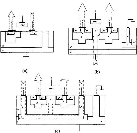
FIG. -4 Simplified classification of basic smart power technologies
(a) Lateral (b) Vertical (c) Quasi vertical (Reprinted with permission from
PCIM Magazine)
6.3 Semi-Custom Smart Power ICs
When quantities cannot justify the cost of a custom circuit and a standard product doesn't quite meet the designer's objectives, a semi-custom circuit can often bridge the cost-performance gap. The design of a semi-custom smart power IC is normally done using the following steps:
(a) System design in the form of a block diagram.
(b) Circuit design for each block in the diagram.
(c) Computer simulation of the designed circuitry, using a simulation program such as SPICE, with the proper model parameters of the various components in the circuit, in particular the power devices.
(d) Modification of the design and additional simulation to verify proper performance.
(e) Additional circuit simulation at the entire temperature range of the device, especially at high temperatures which may be a result of the power dissipated in the power transistors.
(f) Construction of a breadboard and the use of proper "kit parts."
(g) Testing the breadboard at the entire temperature range, especially at elevated temperatures.
(h) Layout of the semi-custom IC, on the properly chosen smart power array.
(i) Generation of two test programs, one for testing the silicon wafers at much reduced current levels and another test program for testing the packaged devices at the desired power levels, in accordance with the specific application.
The 6000 series of semi-custom devices from Cherry Semiconductor Corp. was a good example of the inherent versatility of this type of device. The 6000 array contains two monolithic chips in either a 15-lead multi-watt package or 20- or 24- lead small outline (SO) package ( Fig. 5). One of the chips integrates two power npn transistors, each rated at 50V and 2.5 A. The transistors feature a typical hFE of 80 and a VCE (sat) of 0.75V at a collector current of 2A. Connected in parallel, the two transistors can sink as much as 5A to an external load.
Solitron's semi-custom devices include several array sizes for operating voltages of 20V, 40V, and 80V. Obviously, the smaller arrays include a lower number of small signal components as well as power devices with a lower current rating. Each array is about 50 percent larger than the previous size array and has output devices rated for about twice the Current rating of the previous smaller array. These arrays contain: low power NPN, Schottky PNP, high power NPN, low power PNP and medium power PNP transistors, zener diodes, Schottky diodes, capacitors, and resistors.
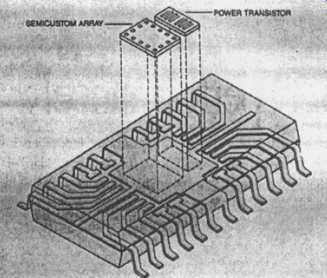
FIG. 5 Genesis 6000 semi-custom array (Cherry Semiconductor
Inc., USA)
The semi-custom array of Fig. 6 is typical of the rest of the family.
Along one edge of the IC, four power NPN transistors occupy about one-third of the die area: small signal components fill the rest. This layout provides good separation between heat-generating and small signal processing components. A designer can use this layout to minimize the thermal effects on small signal components by using balancing techniques, such as cross coupling or centering components.
Along the edges of the chip are 10 x 10 mil bonding pads used for heavy aluminum wires that carry high current from the package pins to the power transistors.
For practical rather than technical reasons, the IC's small signal portion interfaces with similar bonding pads, allowing a single bonding machine to service the entire IC. The silicon area under each bonding pad contains a 7V zener diode that can also function as a 15pF junction capacitor. The area next to the power NPN transistors in the array contains some medium size NPN and PNP transistors. You can use these to form Darlington or even double Darlington connections as well as to form composite PNP connections.
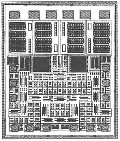
FIG. 6 A photograph of 40V smart power semi-custom array.
The latter is made with a large size PNP transistor that drives a power NPN transistor. The small signal transistors, located in the lower section of the IC, are normally used to form the control circuitry of the smart power design. This circuitry may include digital functions such as logic gates and flip-flops, or analog functions such as operational amplifiers and voltage regulators. An adequate number of resistors, with a binary scale of nominal values, is provided in the vicinity of each transistor to minimize the effort of interconnecting and routing. A predetermined grid is positioned over the entire array area for the purposes of tracing the routing lines.
Using a semi-custom device such as W40E from Solitron, one can implement a smart power relay driver that includes the digital and analog control circuitry as well as the power drive stage, on the same semi-custom IC chip. Fig. 7 shows the block diagram of a smart power relay driver.
7 Smart Power Microcontrollers
In advanced motion control systems, etc. a single-chip microcontroller or microprocessor chip set is usually teamed up with devices capable of processing analog signals and controlling high current loads. These additional devices are either discrete devices or ICs usually constructed in technologies dissimilar to that of the controller IC or to each other. To fully integrate these functions, new IC processes and circuit designs were developed in order to create a single-chip solution for motion and power control applications.
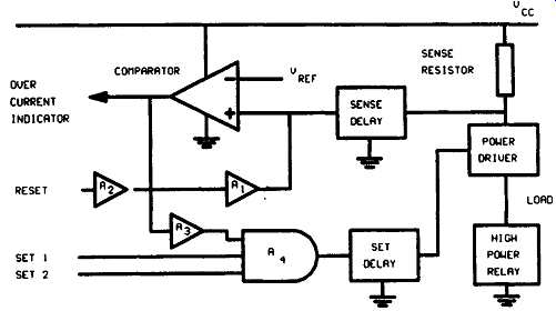
FIG. 7 Smart power relay driver
The merging of analog power and microprocessor technologies on a single chip has resulted in microcontroller units (MCU). Those enhanced towards power control are called Power Controller Units (PCU). By 1990 an initial test device had been produced by Motorola to evaluate this integrated technology. At least four such controllers from Motorola were commercially available by the end of year 1996.
7.1 Architecture of a PCU
The system level block diagram of the PCU is shown in Fig. 8. The main controlling function is provided by the popular 8-bit 68HC05 CPU core supported with 96 bytes of RAM and 2064 bytes of user ROM. An additional 240 bytes of ROM are present to support production testing and self-test functions.
This CPU is a well-known industry standard that contains an 8-bit accumulator and an 8-bit index register. It supports 65 instructions and 10 addressing modes, including an 8x8 hardware multiply, bit testing and bit manipulation. This CPU can support seven levels of interrupts and 64K of memory-addressing space. One CPU bus cycle lasts two cycles of the on-chip oscillator with a maximum bus speed of 4MHz, which yields a typical instruction execution time of less than 1 ~tsec.
The two programmable 8-bit I/O ports provide a total of 16 pins, which can be con figured as either inputs or outputs using a software programmable data direction register. The multipurpose timer provides several timing functions that include an 8-bit free-running timer with overflow interrupt, a pre-scalable real-time interrupt and a computer operating properly (COP) detector.
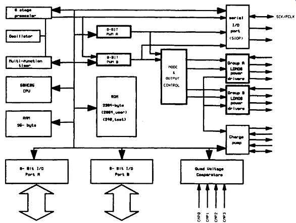
FIG. 8 PCU Overall block diagram (Copyright of Motorola,
used by permission)
The timer is clocked by 1/4th frequency of the CPU bus clock for a maximum count speed of 1 MHz. The real-time interrupt and COP function are driven by the 8-bit free-running timer overflow through a 4-stage software programmable pre-scaler, which provides the following timing for a 4MHz CPU bus clock:
• The free-running timer overflows every 256 ~tsec.
• The real-time interrupt is generated every 4, 8, 16 or 32 milliseconds.
• The COP will reset the CPU in 33, 66, 13 l, or 262 millisec, if not properly serviced by the software.
The serial I/O port (SIOP) is a simple serial interface with a synchronous 8- bit format and simultaneous transmit and receive registers connected to separate pins for data output and data input. The data clock is bidirectional depending on whether the SIOP is programmed as a master or slave device. The order of transmission (MSB or LSB first) and the clock baud rate can be specified with the software code for the ROM. Two pulse-width modulators (PWM) with a common prescaled clock source are provided, as detailed in Fig. 9. These PWMs are implemented in hardware to eliminate the constant attention required by most software-driven PWM schemes.
Each PWM can be programmed with an 8-bit number to provide duty-cycles in steps of 0.4 percent rom 0 to 99.6 percent (255/256). The frequency of operation of both PWMs is set by a single programmable 8- stage prescaler that is clocked from the on-chip oscillator. The maximum PWM frequency occurs when the prescaler is connected directly to the oscillator frequency (divide by 256 overall) and the minimum PWM frequency occurs when the prescaler divides the oscillator frequency by 128 (divide by 32768 overall). For a maximum oscillator frequency of 8MHz the PWMs can run as fast as 31.25KHz.
The minimum oscillator frequency should be at least 1MHz to ensure adequate performance.
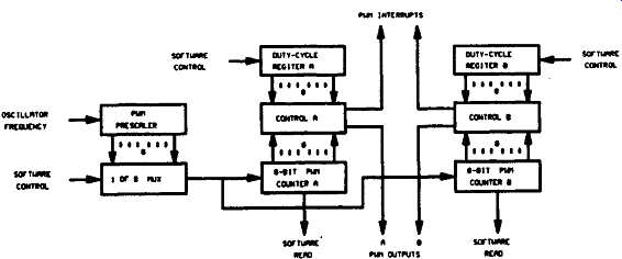
FIG. 9 PWM Block diagram (Copyright of Motorola, used by
permission)
7.2 Commercially Available Devices
Commercially available devices based on the above technology by Motorola are 68HC705MC4, M68HC708MP16, MC68HC16Y1, and MC68332G. The first two of these silicon efficient, cost effective controllers are for brushless DC motors and three phase induction motors, respectively. If a highly flexible general purpose machine is preferred MC68HC16Y1 and MC68332G could be used. These two flexible Time Processing Units (TPU) with 16 channels are actually having separate processor cores for complex timing tasks. Table 2 compares the four devices.
===
TABLE 2 Comparison of Motorola Motor Control Units (Source: Motorola)
Processor core ROM/EPROM RAM Timer A to D converters PWM 68HC705MC4 Application HC05 3.5K 176 16-Bit 6 channel (8-bit)
2 channel (8-bit, 23.4Khz Max)
68HC708MP16 HC08 16K 512 16-Bit 10 channel (8-bit)
6 channel (12-bit)
MC68HCI6YI HC 11 48K 2K 16 Ch TPU 10 channel (8-bit)
16 Channel TPU MC68332G 68000 None 2K 16 Ch TPU None 16 Channel TPU I/O 22 37 95 47 Self Check COP COP WDOG WD(X~ .... Brushless DC motor; General purpose motor control; Induction motors; General purpose motor control
===
7.2.1 68HC705MC4
The 68HC705MC4 is an HC05-based MCU designed for three-phase brushless DC motor (permanent magnet) drive applications. General features include 3.5 Kbytes of EPROM, 176 bytes of RAM, a 16-bit timer, 4 general-purpose I/O pins, and an SCI (UART) port in a 28-pin SOIC or DIP package. In addition the MC4 has specific features that target brushless DC motor control including a 2-channel, 8-bit PWM module; a high current source port; and a 6-channel, 8-bit A/D module. Key features of the 6-pin, 2-channel PWM module include: 16 PWM rates between 122Hz and 23.4KHz for each PWM channel, buffered data registers with an interlocking mechanism for coherent updates of the pulse width outputs on each PWM channel, and a 3 output commutation MUX connected to an output port with 10 mA current sink capability per pin (thus cost reducing the external components required for building motor drives).
7.2.2 68HC708MP16
The 68HC708MP 16 is an HCO8-based MCU designed for open loop three- phase AC induction motor drive applications. General features include 16 Kbytes of ROM, 512 bytes of RAM, 2 16-bit timers, SPI, SCI, (UART), 13 general-purpose I/O, and an LVR module in a 64-pin QFP package. The MP16 also has specific features that target AC induction motor applications including a 6-channel, 12-bit PWM module; a high current sink port; and a 10-channel, 8-bit A/D module. Key features of the 6-channel PWM module include center- or edge-aligned modes, a mode that con figures the six outputs as complementary pairs for coherent updates, a dead-time generation register to prevent shoot through currents in the motor drive circuit, current sense pins to correct for dead time distortion, and fault detect pins for fast shut down of the PWM outputs.
The hardware contained in the PWM module eliminates the need for several external components (i.e. logic for current sense, deadtime generation, and fault handling). Overall the MP16 offers high performance for an affordable price in open loop AC induction motor applications.
7.2.3 MC 68HC 16Y1 and MC 68332G
Timing intensive signals common to motion control applications are easily handled by Time Processing Units (TPUs) in the MC68HC16Y 1 and MC68332G. These 16 channel TPUs are actually separate processor cores dedicated to performing complex timing tasks. They handle a wide variety of motor and motion control tasks with great flexibility. TPU functions such as Hall Effect Decode, Quadrature Decode, Multiphase Commutation, and Stepping facilitate the implementation of motor control designs. Bursky (1996) provides details about 8-bit MCU for automotive system with high current and high voltage drive capability.
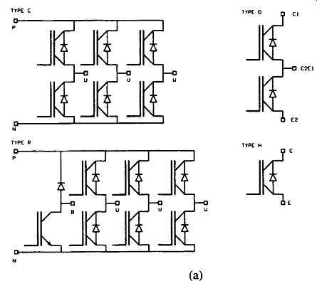
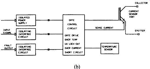
FIG. 10 Intellimod family (Powerex Inc, USA) (a) Configurations
(b) Block diagram
8 System Components and Impact of IGBTs
For building intelligent modules, in principle any turn-off power semiconductor can be used. Therefore, quality control of specific characteristics and a rough estimation of costs for triggering and protection are required first. One can see that the MOSFET and IGBT, which can be triggered almost without any power, offer the very best conditions for an advanced module construction. Their switching characteristics also are more favorable, so that they secure low-loss applications for quite a wide frequency range.
The reduced safe operating area of bipolar elements appears to be a disadvantage when discussing hybrid protection concepts. MOS-devices, however, can be protected by simple and nearly powerless circuits. In addition, they offer the possibility of chip-integrated sensors. The IGBT, which combines above mentioned advantages with low on-state values of bipolar switches for a wide power range, currently is popular for the construction of intelligent power modules. Practical examples of Intelligent Power Modules (IPM) using IGBTs are the Intellimod-3 from Powerex, Inc. USA (Motto and Williams, August and September 1992), ISO- MART from IXYS Semiconductors (IXYS Semiconductors, Technical Information 36). Fig. 10 shows the IPM's internally integrated functions and the isolated interface circuits and control power supply that the user must provide. The internal gate control circuit requires only a simple + 15V DC supply. Specially designed gate drive circuits eliminate the need for a negative supply to off bias the IGBT. The IPM's control input can interface with opto-coupled transistors with a minimum of external components.
Intellimod devices have ratings from 10A to 600 A at 600V and 10 to 300A at 1200V. Fig. 10(a) shows available configurations: C, D, R, and H. A block diagram of an ISOMART half-bridge module is shown in Fig. -11. The IGBTs are driven by a digital 15V CMOS interface, which is galvanically isolated from the main terminals by toroid pulse transformers. On the fight side, one finds the IGBTs with their corresponding free wheeling diode in phase-leg configuration. A specific driver IC (ASIC) includes a low loss gate drive circuit and the control of the gate-and collector voltage of the IGBT. The energy needs by the ASICs is supplied by a controlled SMPS on the logic level side of the IPM. The energy is provided via a toroid transformer. For details on IXYS Semiconductors, Technical Information 36 is suggested.
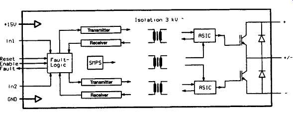
FIG. 11 Block diagram of an ISOMART module (IXYS Semiconductors)
9 Future
For now, most of the action seems to be in medium-level integration, with an emphasis on keeping costs down and efficiently implementing functions, either using a discrete transistor with protection or using a more complex control IC. However, commercialization of these products take 5-10 years of research and development.
Meanwhile, some companies are working on technology to combine BCD processes to better compete with discrete approaches. For example, Siliconix Inc., USA recently unveiled a line of power MOS-FETs that uses a patented vertical-trench structure. If the company could combine such vertical structures with CMOS and bipolar structures (it already has a BCD process), many of the cost and performance tradeoffs between discrete and integrated transistors would disappear. Another interesting development is BCD3 technology, which can integrate EEPROMs. In the future, processes that combine programmability with power may provide the necessary design flexibility to tip the scale toward more complex power ICs.