AMAZON multi-meters discounts AMAZON oscilloscope discounts
1. Introduction
With the introduction of mainframe computers in the 1950s, power system engineers had to take a hard look at energy needs from a quality angle. As systems grew in complexity, it became more apparent to the engineers that the power that kept the systems running was raising havoc, causing equipment failures and corrupting data. As a result, the Uninterruptible Power Supply (UPS) ua back-up to stand between the commercial power supply and the computer R was born. The first uninterruptible power supply equipment, then known as no break power supplies, were of rotary design as shown in Fig. 1. The market at that time for these systems were in mainframe computers, communications, and radar, etc.
During the last two decades there has been a shift from mainframe computer system sales to minis, micros, and portable computers and more recently towards network systems. With this shift, several changes have occurred in the UPS industry. The three decades from 1960 gave birth and evolution to different kinds of static type UPS systems where no rotating electrical machinery was used as major system components.
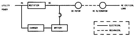
FIG. 1 An old type of a rotary UPS System
The physical size of UPS systems has decreased dramatically. Also, the cost has been reduced from over $2 to $1 per watt. As the world has migrated from the mainframe to the client/server distributed networking environment, the UPS market has shifted from the large multi-module UPS systems to the small single phase UPS systems. As per U.S. industry estimates (PQ Assurance Journal), in 1992 there was a total of US$1.225 billion worth of sales which had a breakdown of US$ 964 million commercial, US$ 245 million industrial and US$16 million residential components. In 1997 these figures were US$ 2.6, 2.1, 0.5 and .027 billion respectively for total, commercial, industrial and residential components. In the year 2002 total sales are expected to rise up to 3.94 billion US$ with 3.17 billion commercial and 732 million of industrial components. Industry estimates further indicate that over 71 percent of the UPS sales are for units less than 30 kVA ratings while 24 percent account for units of the capacity between 31 to 500 kVA ratings. Very large systems with ratings over 500kVA account for the rest.
In 1992, out of total UPS market, only 37 percent was made up of large three phase systems. The 63 percent balance was made up of small single phase UPS units. It was anticipated that by 1997, the UPS market to have large three phase modules will only represent 25 percent of that total with the balance of approximately 75 percent being comprised of small single phase units (Katzaro, 1993). This section provides an overview of UPS systems with particular attention to single phase low power UPS systems used in modern information environments.
2. Different Types of Uninterrupted Power Supplies
Present day UPS systems can be divided in to three basic topologies, namely: off-line, hybrid, and on-line types. Each topology, in turn, can feature one or more technical variations, although the basic operation is about the same within each group. All UPS use an internal battery that produces AC power via an inverter. How and when this inverter comes into play largely determines the effectiveness of the UPS.
2.1 Off-Line UPS
Off-line UPS systems are the simplest forms of back up power systems. A block diagram of an off-line system is shown in Fig. 2(a). The off-line type UPS systems normally operate off-line and the load is normally powered by the utility line. When the utility power excursions are of such magnitude that they are beyond acceptable limits, or fail altogether, the load is transferred from the utility line to the UPS. The actual transfer time is usually very fast, in the sub-cycle range, however, the detection time may be longer and therefore, off-line UPS may not be as reliable as an on-line system.
The major advantage of the off-line UPS systems is lower cost, smaller size and weight and higher efficiency, since most of the time the UPS system is off-line and the load is powered by the utility. However, the disadvantages of the off-line UPS is that switching to the inverter is required when the load is most vulnerable, i.e., upon failure of the normal power source.
Here, the term UPS is really a misnomer because the inverter is normally off.
For this reason off-line UPS are also known as standby power sources, or SPS. Fig. 2(b) indicates the general arrangement of an off-line UPS system.
When the line voltage is within acceptable limits, the load is powered from the input utility supply. During this operation a rectifier block keeps the battery bank charged.
When the input voltage sensor block detects an out-of range input voltage, a relay disconnects the incoming supply and load gets connected to the inverter block.
The only significant advantage of off-line the UPS is low cost. This is possible because the inverter in these systems is normally off so the charging and sense circuits are simple and inexpensive. These units provide no line conditioning or voltage regulation and provide only limited surge and spike protection. During sustained low voltage periods (brownouts) an SPS can inaccurately detect a blackout and prematurely switch onto battery.
If a site experiences sustained brownouts or takes successive low voltage hits, an SPS can completely discharge its battery and "crash" the system. In addition, an SPS switching time increases as the utility voltage decreases. It’s not uncommon for a unit with a 5msec transfer time at 120VAC to exceed 15msec at 100 VAC. Because a brief period of low voltage precedes most blackouts, this may place the system at even great risk. Fig. 2(c) shows the typical oscillograph of a off-line UPS at the transfer.
2.2 Hybrid UPS
These units are nearly similar to the off-line UPS units, but with the addition of a ferroresonant or electronic line conditioner that provides voltage regulation and energy storage (using a resonant circuit) in an attempt to ride through the glitch caused by switching on to the battery. A hybrid UPS with an electronic line conditioner is shown in Fig. 3(a).
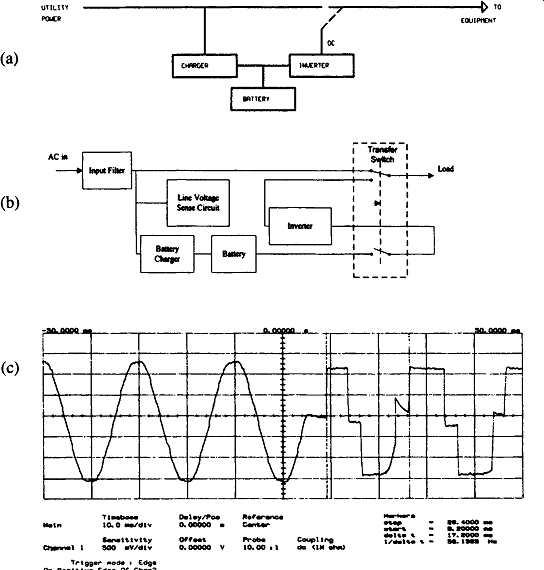
FIG. 2 Off-Line UPS (a) Simplified block diagram of an off-line UPS (b)
Block diagram of an off-line UPS showing the transfer process (c) An oscillograph
of AC output during the transfer process of a typical off-line UPS
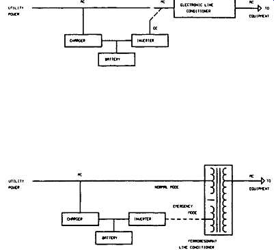
FIG. 3 Hybrid UPS (a) A hybrid UPS with an electronic line conditioner
(b) A hybrid UPS with ferroresonant line conditioner
A hybrid UPS topology (sometimes called "Triport," "Line Interactive," "Utility Interactive," "Electronic Flywheel," "Hot Standby .... Bi-directions," or "No Break") with a ferroresonant line conditioner is shown in Fig. 3(b). Some hybrid UPS systems eliminate or minimize the switching glitch by discharging the storage charge retained on the capacitors on the electronic or ferroresonant conditioner to bleed onto the load line while the unit switches to its battery.
In reality, this "ride-through" concept does not always work. During this switchover the output voltage can drop as much as 35V for a 120V nominal output system. Like SPS, hybrids can misinterpret brownouts as blackouts and prematurely switch to their batteries. Also like SPS, switching time can increase during low voltage conditions, often exceeding the ride-through of the conditioner, as well as the hold up capability of a switching regulator load.
2.2.1 Line Interactive UPS Systems
Bell Labs in the mid 1970s proposed a new technique for UPS applications as shown in Fig. 4(a). This topology, based on an originally patented technique in 1968, referred to as a "triport," uses a ferroresonant transformer with three power ports, two AC input ports (line and inverter) and the AC output port. The first triport was implemented with an impulse commutated SCR inverter which was operational at all times to safeguard against commutation failure at the instant of AC line failure. This guaranteed an operational inverter when battery power was needed to support the critical load. Even though the inverter was always on, its output was adjusted in voltage amplitude and phase to match the AC output. This way, all output power was drawn from the AC input. Since power is flowing into only one port of the triport, it’s classified as a single power path line-interactive UPS. Note that the Bell Labs topology was capable of dual power path operation.
This was called the "share" mode and occurred when the inverter phase was shifted with respect to the AC output. In this mode, AC input and battery power was fed to the output. This mode was only used when transferring from battery power to line power where single power path operation ensued.
With the power semiconductors such as MOSFETS and IGBTs entering the market line interactive UPS system designers were able to replace the SCRs with the newer devices. Early design advancements were to replace the SCRs with power MOSFETS as the IGBTs were expensive.
Many variations to the basic technique discussed above are used in practical systems available in the market as line interactive models. Fig. 4(b) depicts a single phase line interactive UPS with a bi-directional converter. The UPS consists of a three port transformer (triport), a bi-directional converter, two chokes, and a battery.
The bi-directional converter regulates the output voltage when the utility is present, provides output power when the utility fails, and also serves as a battery charger. The converter is large enough to deliver both the rated output power and the battery recharge power (typically 10 percent of maximum output power). The bi-directional converter is a pulse width modulated bridge regulated by two control loops. One loop senses the output voltage and varies the amplitude (pulse width) of the converter AC voltage while the other loop monitors the battery voltage and adjusts the converter phase to charge the battery. Fig. 4(c) is an equivalent circuit of the line interactive UPS.
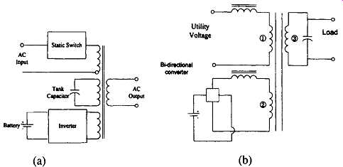
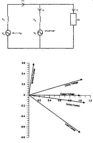
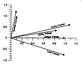
FIG. 4 Triport UPS system (a) Basic block diagram (b) Design using a
bi-directional converter (c) Equivalent circuit of line interactive UPS
(d) Phasor diagram when utility voltage is higher than nominal (e) Phasor
diagram when utility voltage is lower than nominal
It can be shown that the utility current could lag or lead depending on the value of the utility voltage (Handler and Rangaswamy 1989) as per Figs-4(d) and 7--4(e). For further details on triport design Gupta and Handler (1990), Rando (1978), and Handler and Rangaswamy (1989) are suggested.
The triport design was very popular, however it resulted in a UPS that was heavy, noisy and had only limited range for correction for input voltage variations.
Considering this drawback in the triport design some manufacturers such as Liebert Corporation have introduced designs based on auto-transformers. The auto-transformer could be designed with taps that allow correction of mains voltage over a wide range ( Fig. 5(a)). The inverter could drive a winding on the auto-transformer and provide backup when the mains was beyond control. In these designs leakage inductance of the auto-transformer was usefully utilized as an energy storing inductor for the charging mode. By using complex algorithms in the microcontroller subsystem, the inverter could be con figured to run "backwards" and charge the batteries. However the design becomes bit tricky as the transformer needs to be designed with a well controlled built in leakage inductance which could store the proper amount of energy to charge the batteries. The concept is indicated in Fig. 5(b). A simplified block diagram of an auto-transformer based line interactive system is shown in Fig. 5(c). During the charger mode two FETs, Q4 and Q3, switch on, charging the leakage inductance of the auto transformer. In the next cycle Q2 and the body diode of the Q3 switch on, charging the battery. In this case the circuit operates as a two quadrant boost converter. In this case 50Hz FETs are not switched as part of the battery charger control. The microcontroller subsystem which runs a complex algorithm to generate FET drive signals, monitors the battery voltage and charge current and adjusts the converter's conduction cycle maintaining the battery's charging regime within prescribed limits. Compared to the inverter mode where connections T 1 and T 2 serve as the transformer primary winding, these terminals are seen as the transformer's secondary in the charging mode.
Fig. 5(d) indicates the operation of the inverter mode. The power semis Q1 and Q3 are switched by complementary 50 Hz signals which control the UPS base output frequency. Q2 and Q4 are switched by a high frequency signal such as 20 kHz PWM waveform to control the sine wave UPS output. This process is explained in section 3.2.3 as the same technique is used in the on line UPS systems with sine wave output. Fig. 5(e) indicates the waveform at output during the transfer process.
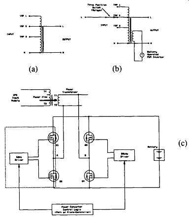
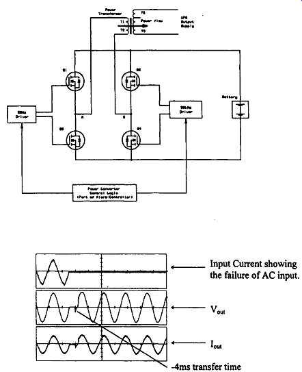
FIG. 5 Line interactive UPS system with an auto-transformer (Courtesy
of Liebert Corporation, USA) (a) Basic auto-transformer (b) Auto transformer
with battery operated PWM inverter (c) Operation in charger mode (d) Operation
in inverter mode (e) Output during the transfer process ma typical waveform.
If the input voltage varies and the transformer output remains in specifications there will be no transfer to inverter mode. When the input sees an over voltage, surge or a spike, associated circuits detect this and transfer the load to battery. When the disturbance is over it will transfer back to mains. If this happens quite often, the UPS may switch back and forth between mains and battery. If this type of mains problem is common, a line interactive UPS may not be the best solution. In this situation an on-line UPS may be required.
A line-interactive UPS will provide all the features of off-line models, with the addition of a "boost" and "buck" feature, which allows the load to be supplied from the mains by providing a low and high voltage mode of operation. Without this feature, the UPS would often be running on battery, and so when a full power failure occurred, the battery would be partially discharged, and the autonomy time may be insufficient for an orderly shutdown. Line-interactive UPS are suited to situations where the supply is prone to sags and surges. Line interactive and off line UPS systems normally draw high crest factor currents from the utility due to the fact that the load is either connected directly to the mains (off line) or connected to the mains through a transformer (line interactive). On line UPS systems on the other hand because of a power factor corrected AC to DC converter, have the capability to draw undistorted (low crest factor) currents which minimize the stress to the power grid.
2.3 On-Line UPS Systems
On-line UPS systems as shown in Fig. -6 are not subject to many basic problems introduced by the previous types. Since they continuously regenerate clean AC power, they provide the highest level of protection available, regardless of utility line condition. A well designed on-line UPS protects against blackouts, surges, sags, spikes, transients, noise, and brownouts. Until recently their one drawback has been a higher price.
These systems have the following useful characteristics:
a) No switching involved
b) 100 percent line conditioning and regulation
c) Good sustained brownout protection
d) Typically sinusoidal output
e) Power factor correction and higher reliability
However, these units have much more complex designs than off-line or hybrid types, while the price, weight, and volume are higher. The inverter of an on-line UPS supplies continuous power to the critical load. Under conditions of overload or loads with high inrush currents which is beyond the capacity of the inverter, the static bypass switch provides mains power to the load. Basic components of an on-line UPS are shown in Fig. 7.
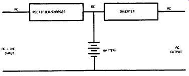
FIG. 6 An on-line UPS
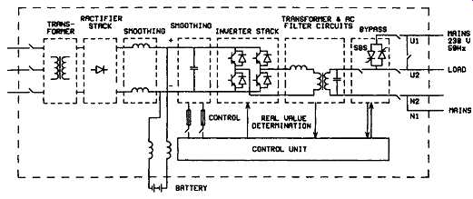
FIG. 7 An on-line UPS system with static bypass, input isolation transformer,
and other blocks
3. UPS System Components
Solid state UPS systems are comprised of several major elements. Those are the (i) rectifier and battery charger, (ii) inverter, (iii) static transfer switch, (iv) logic and control system, (v) battery bank, (vi) diagnostics and communications blocks.
Depending on the capacity and the type of UPS, these blocks may have any thing from a few components to microcontroller or DSP based firmware.
In medium and large capacity online UPS systems a fair amount of modem power semiconductors such as monolithic Darlingtons, power MOSFETS, GTOs, and IGBTs are used currently, while the MCT devices hold a promise for the future. Most of these devices, mounted on specially designed heatsinks, etc., become the power control elements in the rectifier blocks and the inverter. Static switch is usually designed using state of the art thyristors etc., while diagnostic, communication, and control logic is based on simple logic blocks to microcontroller or DSP based systems.
All UPS systems have at least one large, low frequency, magnetic component, usually a transformer. Especially at high powers, even the latest PWM UPS systems require a number of traditional laminated iron magnetics. These are large, heavy, lossy, and expensive, and a great deal of research and development is directed at reducing the quantity and size of these magnetics. Many of the techniques described in this section require the use of high frequency magnetics.
The main advantages of higher frequencies are that acoustic noise can be reduced, and flicker components become smaller. Advances in the design of magnetic materials have not kept a pace with those of semiconductor devices and designs. It’s the magnetic materials which are limiting the speed of high frequency developments, especially at powers greater than about 1 0kVA. In the next few sections individual blocks will be described.
3.1 Rectifiers and Battery Chargers
In low capacity (less than 20kVA) UPS systems, simple single or three phase rectifiers with no voltage control or minimal voltage control are used. However, these simple techniques are not usable with large capacity systems due to harmonic distortion and low power factor which is generally not acceptable by utilities.
The emphasis in all new rectifier designs is to achieve low current distortion at unity power factor. Single phase and smaller three phase UPS invariably use a diode bridge, followed by a high frequency switching stage. The control of this switching stage determines the input characteristics of the rectifier. Modem systems use active rectifiers with IGBTs as shown in Fig. 8.
Such circuits promise active power (displacement) factor compensation, and the possibility of "intelligent" selection of input current characteristics, using IGBTs or Darlington transistors at output ratings from about 10kVA to 50kVA. Modem DSP based designs are sometimes used to achieve the mathematical processing demanded by these circuits, particularly in the high power systems.
Such rectifier circuits are intended for systems using a high voltage (700-800 volt) DC bus, and complement the transformerless inverter designs described later.
However, batteries at these high voltages have inherent disadvantages, and batteries in the 400 to 500 volt range still predominate. These allow standard switchgear to be used, but require conversion up to the high voltages demanded by some inverter techniques. A typical three phase rectifier-battery charger system is illustrated in Fig. 9.
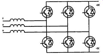
FIG. 8 Three phase active rectifier with IGBT elements
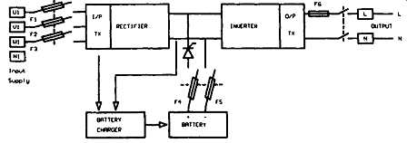
FIG. 9 Typical three phase rectifier-battery charger
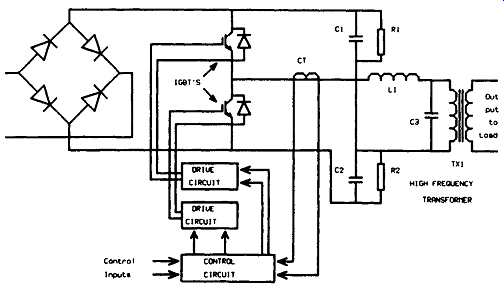
FIG. 10 Resonant DC converter
One trend is towards the use of resonant switching in the high frequency stage, as shown in Fig. 10. Such "soft switching," that is, switching at either zero voltage or zero current, reduces the problems caused by fast switching transients, which, in turn, reduces the RFI generated by these switching stages.
Most three phase UPS systems, especially above about 30 kVA, still use a 6 pulse SCR bridge as shown in Fig. 11(a). This has the disadvantage of low power factor, and high distortion in the range of 30 percent. However filters are available to improve the power factor to above 0.9, and reduce distortion to about 10 percent.
In order to achieve lower distortion a popular technique is the 12 pulse rectifiers as per Fig. 11 (b). This solution, sometimes referred to as a double bridge, can result in distortion between about 12 percent to 5 percent depending on the use of a filter stage (McLennan 1994). Coupled with suitable input isolation transformers it could selectively reduce certain harmonic components and could provide complete galvanic isolation at the UPS input.
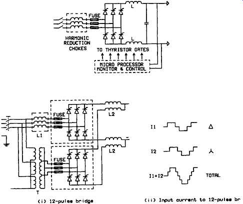
FIG. -11 Charger configurations (a) Six pulse charger (b) Twelve pulse
charger
3.2 Inverters
Historically, inverter debate has focused on Pulse Width Modulation (PWM) and Quasi-Square-Wave (QSW) techniques. QSW is also known as DC Amplitude Control (DAC). PWM techniques are generally popular among low power inverter designs, while DAC is the only static technique applicable at powers in excess of about 500 kVA (McLennan 1994). The discussion in the following sections is restricted to low power PWM techniques.
The basic switching action of inverter systems, irrespective of the power semiconductor switches used, is similar. The bridge usually consists of four main power devices per phase, two of which are switched on at any instant. See Fig. 12(a). On closing S 1 and S 4 current will flow through the load. Conversely, closing S 2 and S 3, current again flows through the load. However, the polarity across the load is now reversed.
In practice, the switches are replaced by power semiconductors and the load by the primary of the output transformer. Fig. 12(b) is a three phase inverter where transistors are used as power switches. The ease with which transistors can be switched on and off gives a considerable advantage over the thyristor based inverters.
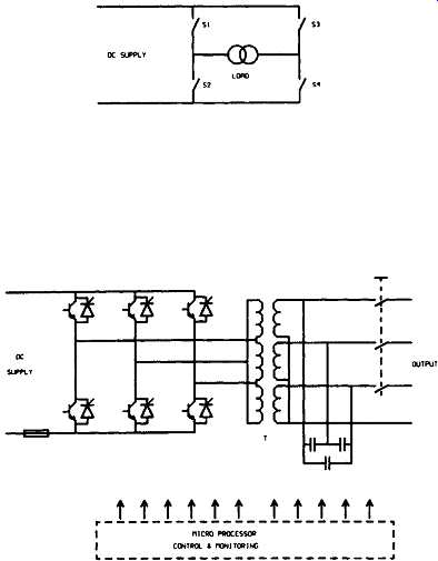
FIG. 12 Inverters (a) Principle of inverter bridge (b) Three phase transistor
Inverter
3.2.1 Inverter Switching Principles
To explain the practical design of inverters, let's refer to Fig. 13(a), where a dual IGBT module is connected to a DC voltage rail. When operating as a switch the circuit has two stable states of interest. The first is when Q 1 is turned ON and Q2 is OFF, whereupon the inverter output is effectively connected to the +ve DC busbar; the second is when the situation reversed, where Q2 is ON and Q1 is OFF and the output is connected to the -ve busbar.
By alternating between these two states the output can be represented in the form of a square wave whose amplitude is dependent upon the DC busbar voltage and whose frequency is determined by the rate at which the transistors change from one state to the other. To ensure that the "off-going" transistor has sufficient time to turn off before the "on-coming" transistor is turned on there is a small delay between the removal of one drive signal and the application of the other; this period is known as the dead band (underlap or the dead time) and is in the order of one or two ItS. Fig. 13(b) depicts the inverter operation when the two transistors are driven by a true square-wave; that is, a gate drive signal having a 1" 1 mark-to-space ratio. This produces a square wave output whose "mean" voltage, with respect to the -ve DC busbar, equals approximately 50 percent of the DC busbar voltage.
Similarly in Figs 13(c) and 13(d) the gate drive signals are shown producing output waveforms having mark-to-space ratios of 3"1 and 1:3 respectively, and the corresponding change in the average voltage is shown to be 75 percent and 25 percent of the DC busbar voltage, as expected.
These diagrams illustrate that the inverter "mean" output voltage can be varied anywhere between 0V and the full DC busbar voltage by controlling the mark- to-space ratio of the transistor drive signals.
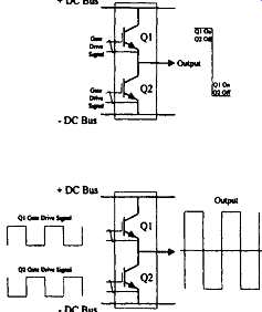
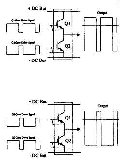
FIG. 13 Illustration of PWM switching principles (a) Basic inverter switch
(b) Inverter switching at 50% duty cycle (c) Inverter switching at 75%
duty cycle (d) Inverter switching at 25% duty cycle.
This principle can be extended to produce a sine wave output by driving the transistors with a drive signal as in Fig. 14(a). However, it’s necessary to filter the high frequency signal using a low pass filter between the inverter bridge output and the load as per Fig. 14(b). It’s important to understand that the drive frequency remains constant and the output voltage is controlled entirely by altering the width of each pulse in the drive train. This technique is the most common inverter technique used in UPS inverters and is called Pulse Width Modulation (PWM). The 50 or 60 Hz AC output is extracted from the PWM waveform by the low pass filter which removes the high switching frequency. In practical systems the switching frequency could be between 2 kHz to over 20 kHz.
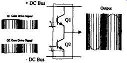
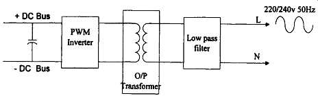
FIG. 14 Pulse width modulation technique (a) PWM waveform to drive the
transistors and corresponding output (b) Filter stage to remove high frequency
components
3.2.2 Selection of Transistors
In recent years manufacturers have been changing over to transistorized inverters compared to older generations which were based on SCRs. Conventional power transistors, Darlingtons, power MOSFETs, or IGBTs are used in modem inverters, depending on the capacity and the inverter design. The power handling capability of transistors is directly related to their physical size, as is their ability to switch at high speeds.
In order to switch high load currents paralleling of transistors or connecting several inverter stages in parallel need be used. Both solutions, however, tend to reduce the reliability owing to the increased component count, and the difficulty in monitoring and controlling the parallel components.
For low power systems power MOSFETs and bipolar Darlingtons are used.
When switching frequencies for the PWM waveform are selected between 2kHz to 5kHz monolithic Darlington modules could be used. With such devices noise levels of not more than 60 dBA could be achieved, which is lower than the noise level encountered in most computer rooms. In order to save costs many practical variations of the basic technique described in the previous sections are used in practical inverters.
IGBTs are the preferred transistors for modem UPS designs. They are significantly more efficient and are easier to control than any other power semiconductors. It’s reported that IGBTs are commonly available for UPS applications up to 750 kVA without paralleling devices, while IGBTs suitable for UPS ratings up to 375 kVA are competitively priced and widely available from multiple sources. Most UPS applications under 50kVA capacity use high frequency PWM techniques in their IGBT based inverters. These inverters could be switched at relatively high speeds such as 20 kHz. The high switching frequency helps improve output dynamic response and helps reduce the cost of magnetics and other components.
While switching losses are significant at these frequencies, overall UPS efficiency in these power ranges are not the most important design goal. Larger UPS systems, over the capacity of about 50 kVA, generally use lower frequency PWM inverters.
These switch at a significantly lower speeds between 2kHz to 5 kHz.
The importance of the switching speed is related directly to the selection of the output filter and the audible noise level produced by the system. If, for example, switching frequency could be above 15 kHz the frequency of the noise produced is above the audible range. The difficulty arises, however, when transistors need be selected, where high currents and a large DC rail voltage need be tackled at high frequencies. Given a nominal DC voltage of about 400 V the corresponding current for systems with ratings of 10-100kVA would be of the order of 30-300 A.
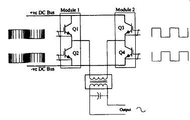
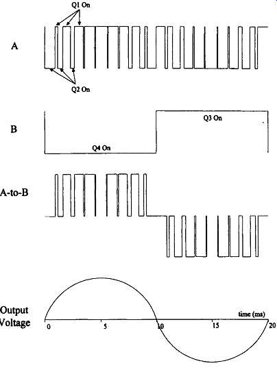
FIG. 15 A practical inverter using IGBT pairs (a) Block diagram (b) Switching
waveforms
3.2.3 Practical Inverter Circuits
The full bridge circuit described could be implemented with many variations depending on the power levels involved and the available transistor modules. One example is shown in Fig. 15 where the two IGBT pairs need not have identical high frequency performance. In this case module 1 is a high frequency type and the module 2 is a low frequency type. As this could save costs of the power semis it’s frequently used in practical systems. In this case Q I and Q2 are switched by a high frequency PWM waveform with a sine wave envelope as described earlier while Q3 and Q4 are switched using a 50 percent duty cycle line frequency waveform. PWM drive signal could be in the range of 10 to 20 kHz.
FIG. 16 Transformerless 4 pole inverter bridge
The IGBTs are switched by two sets of gate drive signals. Q1 and Q2 are switched by the high frequency PWM drive waveform described earlier, and Q3 and Q4 are switched at the line frequency. Thus, considering module 2, for one half cycle of the UPS output Q3 is turned on and one side of the output transformer is referenced (connected) to the positive busbar; and, for the other half cycle, Q4 is turned on and the transformer is referenced to the negative busbar.
Fig. 15(b) shows the waveforms associated and how they are "summed" at the output transformer primary. A dual IGBT package could be used for Q3/Q4 in the same way as for QI/Q2. However, due to its lower switching rate, module 2 does not require such a high frequency specification as module 1. Therefore different types of devices could be used. Module 1 should have fast rise and fall times, to minimize switching losses, and module 2 should be a low Vce(sat ) device to minimize conduction losses.
Referring to Fig. 15(a), this switching arrangement together with the output transformer and filter capacitors generates a sine wave at the line frequency. By feedback control circuits the output voltage amplitude could be regulated.
It’s important to note that due to reasons of matching between load and the inverter/filter stages, the deliverable load power is within a limited power factor range, usually between 0.65 to 0.85. When loads are beyond these specified worst case power factors voltage regulation as well as total harmonic distortion may be affected or tripping or changeover to static by pass may occur.
By the use of microprocessor or DSP blocks a low-power accurate sine wave could be generated and the output waveform from the inverter could be compared in order to produce the necessary feedback control signals. Using suitable gate drive circuits gates or the bases of power transistor could be driven.
Pulse width modulation systems are used up to about 400 kVA due to reasons of low acoustic noise, good voltage waveform, sub cycle regulation and availability of many silicon integrated circuits for pulse width modulation control, which could work in conjunction with microprocessor based control blocks.
The emphasis in modem inverter designs is towards higher efficiencies. High efficiencies lead to improved autonomy times on battery, reduced power losses, and lower power rectifiers. To achieve high efficiency, the optimum balance between switching losses (which increase with increasing switching frequency) and conduction losses (which decrease with increasing switching frequency), must be chosen.
Modem designs are using IGBTs particularly since the new generations of IGBT have progressively lower losses and the ability to switch higher DC voltages. IGBTs are under intense competitive development, and it’s unlikely that any new UPS designs will be released using power Darlington transistors.
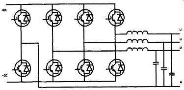
FIG. 16
Recent research papers have proposed the use of transformerless inverters using a 4 pole bridge, as illustrated in Fig. 16. Provided losses in the switching devices can be minimized, and other practical design difficulties overcome, eliminating the transformer will further increase efficiency, and reduce the cost and size of the UPS. For use in 415 volt, three phase systems, transformerless designs require an inverter DC bus voltage of 70(0800 volts. This complements the active rectifiers described earlier.
Despite some recent trends towards lower PWM frequencies, the general trend is still towards higher and higher frequencies, encouraged by associated advances in large magnetic cores. The cost of silicon is reducing rapidly, the cost of copper and iron are increasing, which may see more complex inverter designs specifically to reduce or eliminate transformers and chokes.
3.3 Use of Microcontrollers and Output Voltage Control
In most modem UPS systems a microcontroller is used as the central control element for many primary functions such as: (i) generation of PWM drive waveform, (ii) monitoring the O/P voltage, (iii) inverter output current for overload and short circuit protection, (iv) phase and frequency locking of output and the input power supply, (v) supplying the gate driver stages with properly timed waveforms, etc., in addition to charger control functions. Also, it could carry out many secondary functions such as: (i) providing information display, (ii) fault detection, (iii) battery health monitoring, and, (iv) miscellaneous "intelligence" functions.
Fig. 17 depicts a block diagram of inverter with a simplified block diagram of a control stage. The variable PWM drive signals and line frequency IGBT drive signals are generated digitally by the processor system on the microcontroller block. The precise PWM pattern used is determined by an error detection circuit which monitors the output voltage and either increases or decreases the mark to space ratio of the PWM drive signal, as necessary in order to maintain the correct output voltage.
The processor system monitors the frequency and the phase of the utility voltage for maintaining synchronism between the inverter output and the bypass supply (in-coming mains). Also the control system monitors the inverter current for providing overload and short circuit protection.
Synchronization is carried out by monitoring the zero cross-over point of the utility voltage, which provides the processor with both frequency and phase information. The utility frequency is measured to determine whether or not it’s within the permissible synchronizing window.
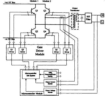
FIG. 17 Inverter stage with processor control
If it’s within the window then the line frequency inverter drive signal is synchronized to the zero crossover signal which keeps the inverter output synchronized with the bypass supply. If the utility frequency is outside the synchronizing window the processor reverts to its internal clock system to provide the line frequency drive waveforms. The current sense signal could be used for various overload protection functions, both software and hardware controlled, depending on the severity of the sensed error. Output capacitors, and RFI filer, etc., are used to provide a clean, harmonic, and interference free sine wave output, which is continuously monitored by the microcontroller subsystem.
3.3.1 Gate Drivers
The gate drivers are used to provide the necessary gate drive signals, when the gate needs a voltage signal (or a charge release) with respect to its corresponding source terminal (of a MOSFET) or the emitter terminal (of an IGBT). In general, the necessary signal may be with or without reference to the -ve voltage rail and creates the need for complex circuits. For this reason, most UPS inverter systems use special gate driver modules or gate driver boards.
As depicted in Fig. 17 a gate driver block contains an individual drive circuit for each IGBT. This module is responsible for providing the necessary drive power and galvanic isolation between the signals leaving the microcontroller block and the IGBT gate/emitter terminals.
3.4 Static Switch
The inclusion of a static switch is an absolute necessity for systems in the medium power (10 to 100KVA) range. It comprise a pair of "back to back" thyristors in each phase of the bypass supply ( Fig. 18) with a parallel contactor.
In the event of overload or failure of the inverter the load would be transferred from the UPS to the mains supply by means of the static switch. In order to achieve this, certain parameters must be met. The two sources, inverter and bypass, must be synchronized and the voltage must be within reasonable limits (_10 percent). Under normal operating conditions the inverter will synchronize with the bypass supply, provided the bypass is within acceptable limits to the load. The tolerance is normally +_.1 percent of nominal frequency (the tolerance range is however, selectable over a range of _+0.5 to +_.2 percent). To ensure no break transfer the phase must be within 3 ° .
If the transfer has been initiated by an overload condition, on the cessation of the overload the load would again be transferred to the inverter. In this manner, the static switch would supply the inrush current normally associated with initial switch on, again avoiding the necessity to oversize the unit.
Theoretically, on-line UPSs provide near perfect isolation between the line input and the load for all types of line disturbance. However, this isolation may be compromised because most on-line UPSs incorporate a static bypass switch, which under certain circumstances connects the load directly to the line input, thus bypassing the unit's rectifier and inverter.
Bypassing the rectifier and inverter is necessary to cope with high transient load currents, such as the inrush current drawn by equipment each time you switch it on. On its own, the inverter is usually unable to cope with these transient currents.
The static bypass switch is also activated if the inverter itself fails for any reason. While this switch is activated, the load is unprotected from any line disturbances unless the bypass circuit itself includes line-conditioning circuitry. In addition, most static bypass switches have a transfer time of a few milliseconds so that each time the switch is activated, load may be deprived of part of an input cycle.
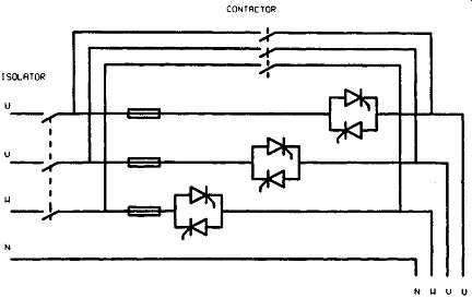
FIG. 18 Arrangement of static switch
4 UPS Diagnostics, Intelligence, and Communications
As in the case of many general industrial electronic systems, modem UPS systems are designed with simple remote alarm panels with associated communication interfaces to sophisticated communication interfaces for network hubs and file server locations, etc. Simple contact signals indicate "on battery" or "low battery" at remote alarm panels at significantly low additional costs.
For communication over short distances (up to about 100m), the remote facility could be hardwired. Over long distances, information could be relayed via modems and phone lines. Most manufacturers are now utilizing the diagnostic and communication facilities to provide remote detailed diagnostics from service locations or the network manager locations, etc.
4.1 Intelligent UPS Systems
An intelligent UPS system has the capability to communicate its status back to the network. With network management software and an intelligent UPS, the network manager can remotely inquire about the UPS operation and the current power condition at the computer site. In addition, the manager can remote control the intelligent UPS and the file server's specific response to a power problem.
Until relatively recently, UPS systems had no "intelligence," meaning that any remote monitoring or control functions could only be obtained by special proprietary circuitry provided by the UPS system manufacturer. The development of client/server network technology introduced the need for communications far beyond what was envisioned previously even for large multi-module three phase systems.
The monitoring and control of very large complex networks developed the need for an open systems standard interface software package that can work with UPS systems of different manufacturers across a variety of diverse operating systems, and in addition, provides system security.
With the simple network management protocol (SNMP) getting widely accepted, UPS designers have developed the communication interferes to interact with SNMP suitably. SNMP includes the capability to monitor and/or control from a central console the network elements (such as servers, gateways, bridges and routers, etc.) as well as a UPS system.
4.2 Levels of UPS Intelligence
There could be several levels of intelligence, as follows:
4.2.1 Level 1
The simplest communications package, UPS monitoring, may be used in a local departmental network. In this case the UPS is connected to the file server or host, allowing the file server to be shut down in the event of a power disturbance.
The basic non-intelligent UPS has simple contact closures that send two messages to the file server or host indicating an "on-battery" or "low battery" condition.
Based on the messages, the network can broadcast the status to the users or initiate an operating system shutdown procedure.
4.2.2 Level 2
Where there are several departmental LANs under the control of one manager, this manager can use the software from any node on the network to monitor and control any UPS system and to switch any device to reset and reboot. By using the RS- 232 protocol, true two-way communication is possible and a much valued feature.
4.2.3 Level 3
In an enterprise network where a number of LANs have been joined together, all critical elements on the network should and can be centrally managed through SNMP.
4.3 SNMP Products
An example of such SNMP products is American Power Conversion's PowerNet SNMP Manager. It provides: (a) A graphical user interface that monitors all UPS units on the network (b) Notification of power alerts to network managers (c) UPS diagnostics (d) Automatic data-save and server-shutdown features upon power failure (e) Scheduled automatic UPS testing (f) Rebooting of locked-up network devices The American Power Conversion package supports Unix with HP Open-View and IBM NetView/6000. Similar network-management UPS software packages are available from Best Power, Clary, and Deltec, with support for Netware, Unix, DOS/Windows, and OS/2 (Travis 1995).
5. UPS Reliability, Technology Changes and the Future
Over the past 10 years, the UPS industry has made substantial improvements in the reliability of its products and systems. The most significant factors effecting the reliability increase are a reduction in component count, higher quality component availability, and the industry's movement toward "proofing" new designs before production. Fig. 19 shows a generalized curve indicating the basic component and topology changes over the years that have led to significant reliability enhancements, primarily due to the component count reduction. At all but the highest power levels, the use of pulse width modulation in place of step wave modulation has permitted the number of power switches to decrease by up to a factor of four.
The evolution of high power Darlington modules and recently the IGBT modules has given the power electronics circuit designer the ability to explore and implement many alternatives for power switches. In addition, these devices have permitted operating frequencies to increase by two orders of magnitude at moderate power levels (60kVA) and up to three orders of magnitude for the desk top products.
Users can expect future UPS offerings to follow the trend of other electronic commodities; smaller, faster, and cheaper. As integration increases, the tendency toward smallness will only increase. Pushing that trend is the fact that several UPS units available now use LtPs and ASICs in their control circuitry.
Both UPS hardware and software promise to undergo major changes in the future. For example, all UPSs now use lead-acid batteries. The main reasons for the choice are cost and power density.
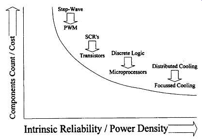
FIG. -19 Technology impact on UPS systems (Source: Burgess 1991) PWM
• Distributed Cooling; ~ Focused ~ Cooling
Intrinsic Reliability / Power Density:
When exotic battery technologies, such as zinc-air and lithium-based designs, decrease in cost, it’s likely they will gradually displace lead-acid units. Other hardware-based improvements expected are more efficient battery chargers and inverters. Power-switching devices are steadily improving in on-resistance, and those improvements will result in lower power losses. As power losses decrease, the use of on-line UPS units will probably increase because of their allure of zero transfer time and simple redundancy.