AMAZON multi-meters discounts AMAZON oscilloscope discounts
1 Introduction
Modem electronic systems are uniquely vulnerable to power line disturbances because they bring together the high energy power line and sensitive low power integrated circuits. The term power conditioning is used to describe a broad class of products designed to improve or assure the quality of the AC voltage you connect to your computer, word processor, automated laboratory instrument, CAD/CAM system, telecommunications system, point-of sale terminal or other sensitive electronic systems.
Utilities realize that different types of customers require different levels of reliability, and make every effort to supply disturbance-free power. However, normal occurrences, most of which are beyond control (such as adverse weather, vehicles running into poles and equipment malfunction) make it impossible to provide disturbance-free power 100 percent of the time. In addition to these external disturbances, sources within buildings, such as switching of heavy equipment loads, poor wiring, overloaded circuits, and inadequate grounding, can cause electrical disturbances. Many of these power disturbances can be harmful to electronic equipment.
Power disturbances can cause altered or lost data and sometimes equipment damage which may, in turn, result in lost production, scheduling conflicts, lost orders, and accounting problems.
There are methods and devices available to prevent these disasters from happening. Protective devices range from those providing minimal protection to those that construct a new power source for critical loads, converting the standard "utility grade power," which is adequate for most equipment, into "electronic grade power" required by some critical loads.
2 Types of Disturbances
2.1 Voltage Transients
Voltage transients are sharp, very brief increases in electrical energy. Spikes are commonly caused by the on and off switching of heavy loads such as air conditioners, electric power tools, business machines, and elevators. Lightning can cause even larger spikes. Although they usually last less than 200 microseconds, spikes can be dangerous to unprotected equipment, with amplitudes ranging from 200V to 2,500V, positive or negative, and sometimes as high as 6,000V. This high magnitude of sudden voltage variation can wipe out stored data, alter data in progress, and cause electronic hardware damage.
2.2 Voltage Surges
Voltage surges are voltage increases which typically last from 15 milliseconds to one-half of a second. Surges are commonly caused by the switching of heavy loads and power network switching. Surges don't reach the magnitude of sharp spikes, but generally exceed the normal line voltage by about 20 percent. This deviation can cause common computer data loss, equipment damage, and erroneous readings in monitoring systems. A surge that lasts for more than two seconds is typically referred to as an overvoltage.
2.3 Voltage Sags
Voltage sags are undervoltage conditions, which also last from 15 milliseconds to one-half of a second. Sags often fall to 20 percent below nominal voltage and are caused when large loads are connected to the power line. Sags can cause computer data loss, alteration of data in progress, and equipment shutdown. A sag that lasts for more than two seconds is typically referred to as an undervoltage.
2.4 Electrical Noise
Electrical noise is a high-frequency interference in the frequency spectrum of 7000Hz to 50MHz. Noise can be transmitted and picked up by a power cord acting as an antenna or it can be carried through the power line. These disturbances can be generated by radio frequency interference (RFI) such as radio, TV, and microwave transmission, radar, arc welding, and distant lightning. Noise can also be caused by electromagnetic interference (EMI) produced by heaters, electric typewriters, air conditioners, coffee makers, and other thermostat-controlled or motor-operated devices.
Although generally not destructive, electrical noise can sometimes pass through a power supply as if it were a signal and wipe out stored data or cause erroneous data output. Problems result when microelectronic circuitry is invaded by transient, high-frequency voltages collectively called "line noise" which can be grouped into one of two categories; normal-mode or common-mode.
2.4.1 Normal-Mode Noise
Normal-mode noise (sometimes referred to as transverse-mode or differential- mode noise) is a voltage differential, or potential, that appears briefly between the live wire and its accompanying neutral. As the name implies, these two lines represent the normal path of power through electric circuits, which gives any normal- mode transient a direct route into sensitive components and therefore the opportunity to destroy or degrade those components.
At today's levels of semiconductor density and sensitivity, normal-mode transient voltages can start causing degradation at around 10 volts, and can cause destruction at 40 volts. These levels may well drop further as semiconductor density increases.
2.4.2 Common-Mode Noise
Common-mode noise is a similar brief voltage differential that appears between the ground and either of the two supply lines. Common-mode transients are most often the cause of disruption, because digital logic is either directly or capacitively tied to the safety ground as a zero-voltage data reference point for semiconductors. As a result, transient common-mode voltage differences as small as 0.5V can cause that reference point to shift, momentarily "confusing" the semiconductors.
2.5 Blackouts
Blackouts result in a total loss of power. Power outages can last from several milliseconds to several hours. Blackouts are caused by many circumstances including vehicle, animal, or personal contact with power lines and equipment, tripped circuit breakers, equipment failure, and adverse weather.
3 Different Kinds of Power Protection Equipment
The power protection equipment can be basically divided into two primary types. They are power enhancement equipment and power synthesis equipment.
3.1 Power Enhancement Equipment
Power enhancement equipment modifies and improves the incoming waveform by clipping, filtering, isolating and increasing or decreasing voltage. The common types of power enhancement equipments are: (a) Transient voltage surge suppressors (TVSS) (b) Voltage regulators (c) Isolation transformers (d) Line conditioners
3.1.1 Transient Voltage Surge Suppressors
One or two decades ago, transients were thought to be non-existent, not to be concerned with, figments of the imagination of persons who would sell unnecessary protection for an imaginary problem. The education and experience of the last decade have clearly demonstrated that this is not the case.
Virtually every user of electricity is affected by transients causing unexplained data losses and scrambled data on computers, excessive lighting replacements, excessive motor insulation deterioration, and much more. Heavy duty motors, sensitive medical equipment, personal computers, office equipment, and even household appliances are all equally subject to the damaging effects of transient activity. Transient activity can be divided into external sources and internal sources.
3.1.1.1 External Sources of Transient Activity
Power companies do everything possible to provide their customers with clean, steady power. Utility systems are designed to provide reliable bulk power.
However, it’s not feasible for them to provide continuous power of the quality required for a completely undisturbed computer operation. Also it should be noted that many pieces of equipment other than computers can benefit from disturbance-free electricity.
Power companies have no control over transients induced by lightning or high power switching at substation levels. Fig. 1 illustrates the enormous energy content of a typical lightning waveform. Currents from a direct or indirect strike may enter conductors of a suspended cable or enter a buried cable by ground currents.
Either way, the surge will propagate in the form of a traveling wave bi-directionally on the cable from the point of origin. Severity of impact to the end user is directly proportional to the proximity of the lightning strike. If the facility is at a 10 to 20 pole distance from the strike, little harm will occur, since the surge current will have been dissipated by the utility ground system. Such is not the case where the strike is much closer. In this case, the residual current can migrate through the facility's service equipment and cause severe damage.
Other externally generated transients result from switching in nearby industrial complexes which can send transients back into the power line, causing damage to equipment.
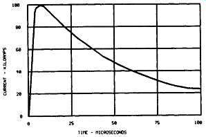
FIG. 1 A typical lightning current waveform
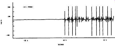
FIG. 2 Transients generated by turning off a fluorescent light
3.1.1.2 Internal Sources of Transient Activity
Internally generated transients result from switching within the facility. Any time the flow of electricity is altered, such as in the simple act of turning a motor or light on and off, transient activity can result in an "inductive kick." An excellent example of this phenomenon can be seen in Fig. 2. It shows the transients generated by turning off a fluorescent light.
3.1.1.3 Transient Energy
The energy of a transient waveform may be readily calculated for transients that are internal to the circuit, such as those caused by inductive switching.
Transients external to the circuit are more difficult to quantify. The energy absorbed by the suppression element may be approximated by:
T E =fVcI~dt t6
Where E = Energy in joules V c --Clamping voltage in volts Ip = Peak pulse current in amperes x = Impulse duration
3. 1. 1.4 Practical TVSS and Performance Considerations
Technologies available today for transient overvoltage protection consist of metal oxide varistors (MOVs), gas discharge arrestors (commonly known as gas tubes), or solid state devices (TVS diodes and TVS thyristors). Each type of device is designed to serve a specific application.
Gas Tubes
Gas tubes are devices that employ an internal inert gas that ionizes and conducts during a transient event. Because the internal gas requires time to ionize, gas tubes can take several microseconds to turn on or "fire." In fact, the reaction time and firing voltage are dependent on the slope of the transient front. A circuit protected by a gas tube arrestor will typically see overshoot voltages ranging from a few hundred volts to several thousand volts.
Metal Oxide Varistors (MOVs)
MOVs are devices composed of ceramic-like material usually formed into a disk shape. High transient capability is achieved by increasing the size of the disc.
Typical sizes range from 3 to 20 mm in diameter. MOVs turn on in a few nanoseconds and have high clamping voltages, ranging from approximately 30V to 1.5kv.
Solid State Devices
TVS thyristors are solid state devices constructed with four alternating layers of p-type and n-type material. The resulting device is capable of handling very high pulse currents. These devices respond in nanoseconds and have operating voltages that start at about 28V and up.
TVS diodes are solid state p-n junction devices. A large cross sectional area is employed for a TVS diode junction, allowing it to conduct high transient currents.
These diodes respond almost instantaneously to transient events. Their clamping voltage ranges from a few volts to a few hundred volts, depending on the breakdown voltage of the device. The fast response time of the TVS diodes means that any voltage overshoot is primarily due to lead inductance.
Table 1 compares the characteristics of the most widely used TVS devices
===
TABLE 1 Comparison of TVS Devices Suppression Element Gas Tube MOV TVS Diodes TVS Thyristors Advantages
• Very high current-handling capability
• Low capacitance
• High insulation resistance
• High current-handling capability
• Broad current spectrum
• Broad voltage spectrum
• Low clamping voltage
• Does not degrade
• Broad voltage spectrum
• Extremely fast response time Disadvantages
• Very high firing voltage
• Finite life cycle
• Slow response times
• Non-restoring under DC
....
• Gradual degradation
• High clamping voltage
• High capacitance
• Limited surge current rating Expected Life Limited Degrades
• High capacitance for low voltage types Long Limited
• Does not degrade
• Fast response time
• High current handling capability
• Non restoring under DCi
• Narrow voltage range
• Turn-off delay time Long
===
TVS device protection levels may be divided into three categories namely: (i) primary protection, (ii) secondary protection, and (iii) board level protection.
Primary Protection
Primary protection is for power lines and data lines exposed to an outdoor environment, service entry, and AC distribution panels Transient currents can range from tens to hundreds of kiloamps at these sources Secondary Protection
Secondary protection is for equipment inputs, including power from long branch circuits, internal data lines, PBX, wall sockets, and lines that have primary protection at a significant distance from the equipment. Transient voltages can exceed several kilovolts with transient currents ranging from several hundred to several thousand amps.
Board Level Protection
Board level protection is usually internal to the equipment; it’s for protection against residual transient from earlier stages of protection, system generated transients, and Electro Static Discharge (ESD). Transients at this level range from tens of volts to several thousand volts with currents usually in the tens of amps.
3.1.1.5 Practical Surge Protection Circuits
MOVs, TVS diodes, and thyristors are available from many suppliers and have well established properties. The extremely fast clamping speed of TVS diodes may be combined with the high current handling capability of MOVs to provide optimum transient protection on AC lines. Fig. 3 indicates four different kinds of TVSS circuits.
(a) Basic circuit of a multi-stage surge suppressor using MOVs, power zeners, and series inductors for power line surges (b) Telecom line protection using gas discharge tube, MOVs, and zener diodes.(c) Line driver/receiver protection (d) Genetic IC protection
Basic circuit of a multistage surge suppressor for power lines is shown in Fig. 3 (a). For surges coming in on the line terminal, the current is shared by M 1 and M 2. The current is returned down the neutral and ground wires back to the AC breaker panel and building ground. Since the impedance of the wires for fast-rising spikes could be greater than that of the MOVs the wire impedance determines the current division. Since the neutral and ground wires back to the panel are typically the same size and length, current would normally be shared roughly equally. Thus, the 3000A test pulse may result in approximately 1500A pulse current into M 1 and M 2.
For short pulses, T 1 and T 2 don’t absorb large amounts of the surge, since the L.dI/dt voltage developed across L 1 makes the first-stage MOVs absorb most of the current. The second-stage MOVs reduce transmitted surge voltage to well below the voltage across MI.
Fig. 3(b) indicates telecommunication protection elements and Fig. 3(c) indicates the use of transients protection zener diodes such as Motorola 1.5 KE series being used for line driver/receiver protection. Fig. -3(d) depicts the generic IC protection.
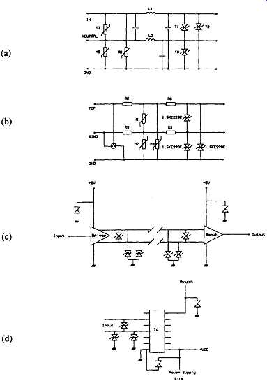
FIG. -3 Protection circuits for transient surges
3.1.1.6 Transient Protection Standards "
Committees such as ANSI, IEEE, and IEC have defined standards for transient waveshapes based on the threat environment. European or IEC transient standards include:
• IEC 1000-2 for Electro Static Discharge
• IEC 1000-4 for electrical fast transients (EFT)
• IEC 1000-5 for electrical transients U.S. transient standards include:
• ANSI/IEEE C62.41-1991 for power line transients
• FCC Part 68 for telecommunication lines
• UL 1449, and various military standards
Regardless of the standard, the transient waveshape is usually defined as an exponentially decaying pulse or a ring wave (damped sinusoidal) for electrical surges. The exponentially decaying open circuit voltage and short circuit current waveforms are shown in Figs-4(a) and 6-4(b), respectively.
The impulse waveform is specified by its rise time and duration. For example, an 8 x 20psec impulse current would have an 8psec rise time from 10 percent of the peak current to 90 percent of the peak current and a 201asec decay time as measured from the start of the virtual front to a decay to 50 percent of the value of peak current. The ring wave results from the effect of a fast rise time transient encountering the impedance of a wiring system.
The waveform shown in Fig. -4(c) is a 0.5psec 100kHz ring wave. The waveshape is defined as rising from 10% to 90% of its peak amplitude in 0.51asec and decaying while oscillating at 100kHz. Each peak is 60 percent of the amplitude of the preceding one. Most component data sheets define the surge capability of a suppression device using an 8 x 201asec or 10 x 10001asec impulse current waveform.
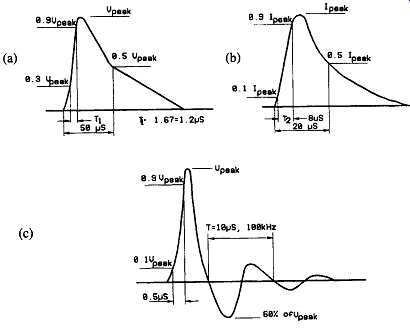
FIG. 4 Surge waveforms (a) Open circuit voltage waveform (b) Discharge
current waveform (c) Ring waveform
3.1.1.7 IEEE C62.41-1991: "IEEE Recommended Practice on Surge Voltages in Low Voltage AC Power Circuits"
IEEE C62.41 identifies location categories within a building, described as A 1, A2, A3, B l, B2, and B3 for surge locations. The "A" and "B" location prefixes represent wiring run distances within a building, the "l," "2," and "3," suffixes represent surge severity. "A" category locations receive their power after more than 60 feet of wiring run from the main power service entrance, with frequent exposure to comparatively low energy surges.
These low energy surges are created when internal equipment cycles on and off, collapsing the magnetic field around the lengthy building wiring carrying the current. The collapsing magnetic field induces surge voltage in the wires proportional to the current being carded by the wiring and the length of wiring.
External surges will be of a lesser threat in "A" locations than "B" locations due to the impedance protection provided by the inductance of the building wiring in "A" locations. IEEE specifies a low energy "ringwave" surge waveform for the "A" locations.
"B" category locations are within a building, close to the power service entrance, with greater exposure to infrequent, high energy surges originating outside the building. The "B" location category surges can be caused by lightning, power outages due to storms, and normal utility switching functions. A "combination wave" with high surge energy is specified by IEEE for these "B" locations.
"1," "2," and "3" denote low, medium, and high exposures respectively, in terms of the number and severity of surges, with "1" being the least severe and "3" being the most severe. A "B3" location, therefore, would have the highest exposure to surge energy, while a "A 1" location would have the lowest incidence of surge energy.
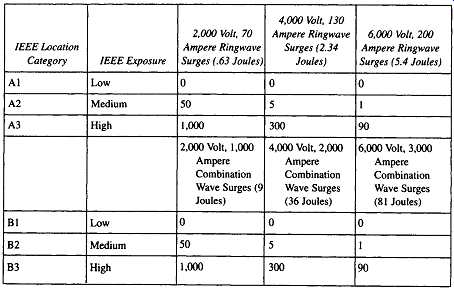
TABLE 2 C62.41 Location Categories, Frequency of Occurrences and Surge
Waveforms
===
IEEE Location Category IEEE Exposure 2,000 Volt, 70 Ampere Ringwave Surges (.63 Joules)
4,000 Volt, 130 Ampere Ringwave Surges (2.34 Joules)
6,000 Volt, 200 Ampere Ringwave Surges (5.4 Joules)
===
Table 2 shows possible annual surge magnitudes, frequency of occurrences, and surge waveform as extracted from the IEEE C62.41 Standard. Fig. -5 depicts the building locations.
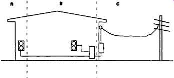
FIG. -5 Building locations and C62.41 categories
3.1.1.8 UL 1449
Several years ago, Underwriters Laboratories established a uniform TVSS rating system by creating UL Standard 1449-1987. Although somewhat limited, it was the first step toward establishing benchmarks by which to compare TVSS products.
Underwriters Laboratories established specific test criteria to determine the ability of a TVSS product to stop the travel of a transient voltage surge into protected equipment.
Underwriters Laboratories divided TVSSs into two categories: plug-in or cord-connected devices and hardwired or direct-connected devices. TVSS devices included in the plug-in and cord-connected category are subjected to a maximum transient surge impulse of 6000V with a short circuit current of 500A available. The voltage available is in a 1.2 by 501as waveform and the current is available in an 8 by 201as waveform. Devices included in the hardwired category are subjected to an impulse of 6000V with 3000A available in the same type of waveform (Lewis 1995). Underwriters Laboratories Inc. has recently proposed revised testing procedures for UL 1449 ( Hartford 1996).
3.1.1.9 Electrostatic Discharge and Circuit Protection
Recent years have seen various standards developed for testing the ESD capability of semiconductor products. These standards have been generated with regard to a specific need related to the electromagnetic compatibility of the system environment. They include the Human Body Model (HBM), Machine Model (MM) and the Charged Device Model (CDM). Each such standard relates to the nature of electrostatic discharge generated within a system application and the potential for damage to the IC. Among the better known standards are:
• Human Body Model using the MIL-STD-883, Method 3015.7
• Machine Model using EIAJIC121
• Human Body model using the IEC 1000-4-2 standard
Testing for ESD immunity is more broadly defined to include a device, equipment, or system. Both direct contact and air discharge methods of testing are used with four discrete steps in the severity level ranging up to 8KV and 15kV, respectively. In its simplest form, the Fig. ~(a) test circuit provides a means of charging the 150pF capacitor, R C, through the charge switch and discharging ESD pulses through the 330ff] resistor, R D, and discharge switch to the Equipment or Device Under Test. The test equipment for the IEC 1000-4-2 standard is constructed to provide the equivalent of an actual human body ESD discharge and has the waveform shown in Fig. -6(b).
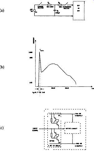
FIG. -6 IEC 1000-4-2 testing (a) Simplified IEC l(XX)-4-2 test energy
source (b)
Typical waveform of the output current of the HBM ESD generator (c) SP 720 implementation for active circuit protection showing one out of 14 cells. (Copyright by Harris Corporation, reprinted with permission of Harris Corporation Semiconductor Sector)
Recently, semiconductor manufacturers such as Harris Semiconductors have introduced SCR diode arrays for semiconductor circuit protection. These devices cater for ESD protection requirements. The SP720, SP721, and SP723 are protection ICs with an array of SCR-diode bipolar structures for ESD and overvoltage protection of sensitive input circuits. They have two protection SCR-diode device structures per input. See Fig. -6(c). The SCR structures are designed for fast triggering at a threshold of one +VBE diode threshold above +V (positive supply terminal) or a -VBE diode threshold below V- (negative or ground). A clamp to V+ is activated at each protection input if a transient pulse causes the input to be increased to a voltage level greater than one VBE above V+. A similar clamp to V- is activated if a negative pulse, one VBE less than V-, is applied to an input.
3.1.1.10 Practical Considerations
The market offers an almost endless variety of makes and models of transient-voltage surge suppressors. However, many manufacturers provide virtually no written specifications to describe the performance of their devices, while others offer exaggerated claims (Steinhoff 1991).
Most designers of electronic equipment, and manufacturers of surge protection devices, use metal-oxide varistors (MOV) and solid state devices (like bidirectional zener diodes) as voltage limiting devices. These devices are available from various suppliers, and have well established properties. Ordinary surge protectors simply divert surges from the hot line to the neutral and ground wires, where they are assumed to flow harmlessly to earth, the ultimate surge sink. These surge suppressors use MOVs and/or other similar shunt components which sense the high voltage of a surge, and quickly change state from an open (non-conducting) circuit, to a very low impedance short circuit for the duration of the surge. When the surge voltage disappears, the MOV returns to an open circuit.
In this way, the protector diverts mainly the surge energy and not significant amounts of power line energy because of the short duration of the surge, unless the MOV has degraded in its normal wear out process to the point where it "clamps" on the power line. When that happens, the MOV explodes and fails, leaving the surge protector unable to provide any protection.
3.2 Voltage Regulators
In AC voltage regulators the limited range of regulation can be anything from less than 1 percent change, over a given line, and load variation range, to 10 percent or greater, depending on the need and the technology implemented.
3.2.1 Motor Driven Variacs
The oldest and most simple type of automatic voltage regulators are the motor driven variacs, where the tap setting of a transformer is changed with the feed back signal from an output monitoring circuit. Even though these are used in many sites they are very slow, bulky, and sometimes have reliability problems.
3.2.2 Electronic Tap Changers
Another more practicable type with light weight and low cost are the electronic tap change systems. Electronic tap changers are electronically controlled devices designed to compensate for line-voltage fluctuations by sensing and switching buck or boost taps to vary the primary-to-secondary turns ratio of a power transformer (see Fig. 7). Tap-changers are more efficient (low 90 percent range), cooler, and quieter than ferroresonant Constant Voltage Transformers (CVTs), with better output stability. However, they lack the ruggedness of the CVT, and are accordingly less often considered as an industrial alternative.
There are two main types of tap-changers. The more popular design incorporates an isolation transformer. It also provides good common-mode noise attenuation but suffers high output impedance. The less popular is based on the auto transformer, which provides low output impedance but lacks in isolation and noise protection. Under certain conditions, both types can exhibit a response known as "tap dancing," in which input oscillates between taps, continually "notching the line," and creating unstable voltages that can damage SCRs and other control electronics.
Electronic tap-changers generally don’t recover well from line notches.
Some microprocessor-controlled units drop their output for several line cycles after a half-cycle interruption. In some designs, a line drop below the tap-changer's low-voltage threshold (which can occur during a severe brownout) can cause the sensing/switching electronics to shut the regulator off as a self-protective measure. In either case, the tap-changer in effect creates its own blackout, allowing its load to crash. One other problem inherent in electronic tap-changers is that their electronic sensing and control systems are necessarily exposed to raw line power. Therefore, they are vulnerable to the same line noise and transients they are supposed to guard against.
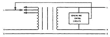
FIG. 7 Block diagram of an electronic tap changer
3.2.3 Thyristor Driven AC Regulators
SCR controlled AC regulators are also a low cost light weight implementation. The most common form of thyristor circuit for AC voltage control is shown in Fig. 8(a) (the thyristors could be replaced by a triac). This has been widely used in applications such as lamp dimmers, where a wide control range is required for loads tolerant to high levels of distortion.
The simple phase control circuit of Fig. -8(a) won’t meet the requirement of producing a nominal output level. This will require the introduction of an auto transformer as shown in Fig. 8(b). For an rms output voltage equal to the nominal supply voltage (rms value of V o) the thyristor firings must be delayed by about 95 ° when the supply is at its maximum (1.2Vo). This delay reduces to zero if the supply is reduced to its lower limit (0.8Vo). There could be many variations to this basic implementation in the practical voltage regulators.
FIG. 8 Thyristor control (a) Simple thyristor phase control and output waveform (b) Single tap regulator (c) Two tap regulator and output waveform
This form of regulator introduces considerable distortion in the output voltage. Under the worst condition, when the supply is at 1.2V o and thyristor firing is held back by about 95 ° , the total distortion is over 50 percent. Even if the regulation range of the regulator were reduced to +_ 5 percent the distortion would still be over 20 percent.
The use of two taps on the auto transformer as shown in Fig. 8(c) results in very significant improvements in regulator performance. Its operation when feeding resistive loads is simple. At the start of each half cycle one of the lower thyristors conducts, supplying voltage to the load. Some time later in the half cycle, one of the upper thyristors is triggered. This increases the voltage on the load and by so doing commutates the lower thyristor. At the end of the half cycle, the upper thyristor is extinguished.
The output voltage can be continuously varied between the two values available at the transformer taps by altering the time of triggering the upper thyristors. The distortion is considerably lower than the single tap circuit, being zero at both extremes of input voltage and about 15 percent for the worst condition. There will be proportionally lower distortion if the regulation range is reduced below _ 20 percent.
Thyristor regulators when used on inductive loads could cause special transient situations, which may stress the thyristors. This type of situations and the inherent waveform distortion on basic thyristor regulators make these less popular than some other types, unless these are further buffered by special output filters, etc.
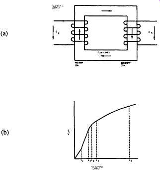
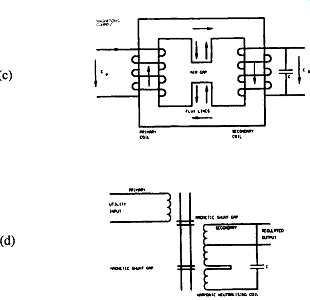
FIG. 9 Comparison of ferroresonant transformer and conventional transformer
3.2.4 Ferroresonant Regulators
Ferroresonant transformer or constant voltage transformer (CVT) has been commercially available for over four decades.
(a) Conventional Transformer (b) Flux vs. Magnetizing current (c) Ferroresonant transformer-basic arrangement (d) Ferroresonant transformer with a harmonic neutralizing coil
The easiest way to describe a ferroresonant transformer's operation is to compare it with an ordinary power transformer ( Fig. 9 (a)). If a typical transformer operates at a high enough primary current, its core becomes saturated with flux lines. Increasing the primary current won’t then increase the secondary voltage.
Consequently, operating an ordinary power transformer in saturation will create a voltage regulator, though such operation is impractical because primary saturation current is very close to a short circuit. Normal current in the I1-12 region shown in Fig. 9(b) causes a linear change in flux, but once the current reaches saturation region (I4-I5), the resulting flux changes are small. To the left of the point 13 , flux changes are in direct proportion to primary current: to the fight of the 13 , the curve becomes non-linear and changes in current have less effect on flux.
The ferroresonant transformer, on the other hand, is designed to operate in saturation ( Fig. 9(c)). However, since it’s the secondary coil that operates in saturation, not the primary, more flux must be produced in the secondary core leg than in the primary. The core structure is modified by the addition of a magnetic shunt to loosen the coupling between primary and secondary. Because of the air gap in the shunt, the core section has a high reluctance and the main path for magnetizing flux is through the outer core. As the input voltage increases, the magnetizing flux through the core section increases, and with it, the inductance of the secondary winding. The addition of an output capacitor alters this.
Once the reactance of the winding equals that of the capacitor, the two resonate, producing a higher output than the turns ratio voltage alone. This effect is similar to a series resonant circuit where point of resonance increases the voltage across the capacitor substantially above the impressed voltage.
The output waveform of a basic ferroresonant transformer will be like a square wave (due to flattened top) and is suitable for many loads, but may not satisfactorily provide power for some electronic loads without the addition of a harmonic filter choke ( Fig. 9(d)). With this filter, a large part of the output harmonic content is canceled producing a sine wave voltage with reasonably low total harmonic content.
A properly designed conditioner could regulate the output voltage to _ 2 percent or __. 3 percent. With the input varying as much as __ 20 percent, the output total harmonic distortion should be no greater than 5 percent or 6 percent.
One of the advantages of ferroresonant transformers is their ability to attenuate normal mode noise voltage transients. This attenuation is up to 10 times more than conventional tap changer regulators provide. Since the secondary winding operates in saturation, transients and spikes are clipped. A ferroresonant transformer has some very desirable overload characteristics. If the output is short circuited, the current increases by only about 80%. A well designed ferroresonant transformer can maintain a short circuit indefinitely.
Note that the ferroresonant transformer is a tuned circuit, which is frequency sensitive. Typically, a 1 percent change in frequency produces a 1.5 percent change in output voltage. Another draw back of ferroresonant transformers are their low efficiency, particularly at the no load and low load conditions.
Fig. 10(a) describes the operating characteristics typical for a ferroresonant line regulator for input voltage versus load power factor. Fig. 10 (b) shows the output voltage versus percent load. These curves are not intended to describe the technology in total capability, but rather are presented to show the typical performance of a particular design.
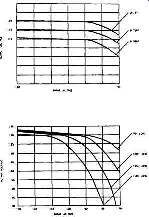
FIG. 10 Characteristics of ferroresonant regulator (a) Output voltage
vs. power factor for a ferroresonant regulator (b) Output voltage vs percentage
load for a ferroresonant regulator
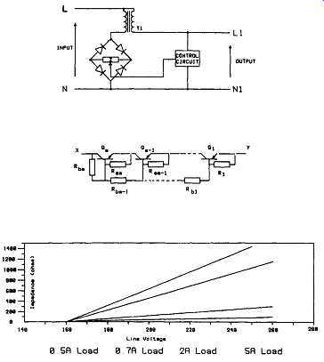
FIG. 11 BJT array based AC line regulation (a) Basic technique (b) Arrangement
of the multi-element transistor array (c) Impedance of transistor array
vs line voltage and load current
3.2.5 Other Types of Voltage Regulators
Within the past several years, new solid state techniques were proposed for AC line voltage regulation, as well as power conditioning. Some of these techniques are based on bipolar power transistor arrays with simple buck-boost transformers as shown on Fig. -11.
Simplified block diagram of such an AC voltage regulator is shown in Fig. 12. Basic techniques used for the conditioner could be explained using Figs11 (a) and (b). Referring to the block diagram in Fig. 11 (a) primary of a buck-boost transformer T1 is connected in series with a bridge rectifier and an impedance Z. Impedance Z created by a multi-element bipolar power transistor array as per Fig. 11 (b) is controlled by a feedback control circuit which is designed using low voltage solid state circuitry. Bridge avoids voltage reversals across the bipolar power transistor array. As per configuration shown in Fig. 11 (b) the effective impedance across the transistor array is dependent primarily on the components R b and R e (Kularatna 1988, 1990, and 1993). In the practical implementation of the technique Re I to Rem could be implemented with transistor elements of a multistage opto isolator. Fig. 11(c) shows the required impedance across the array V s input voltage and output load current.
The low voltage components used for feedback control and other functions are placed in isolation from the line voltage handling blocks and this improves the reliability of the design. Further, this technique does not have sensitivity for line frequency variations or power factor etc. and waveform fidelity (of the basic implementation itself) is far superior to ferroresonant systems. Also the technique could be easily modified to provide harmonic control, where transformer design itself is truly simple compared to a ferroresonant transformer. This technique is easily applicable for VA ratings from 200VA to 3KVA and can be easily mixed with electronic tap changers (for efficiency improvement purposes rather than regulating purposes) as discussed in Kularatna (1988, 1990, and 1993). Another new approach to AC line voltage regulation by switched mode techniques is described in Zhang (1994) and Bhavaraju and Enjeti (1993).
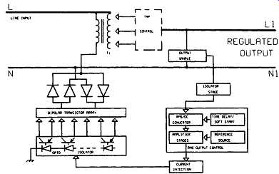
FIG. 12 Block diagram of a practical voltage regulator based on bipolar
power transistors --REGULRTED OUTPUT
3.3 Isolation Transformers
Isolation transformers are specially designed transformers that attempt to limit the coupling of noise and transient energy from the primary side to the secondary side by "isolating," or physically separating those two windings, and adding electrostatic shielding bonded to the ground wire (see Fig. 13).
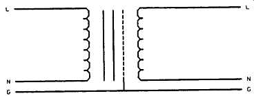
FIG. 13 Isolation transformer
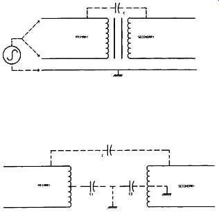
FIG. 14 Effect of coupling capacitance (a) Capacitor C providing a direct
path for common-mode noise (b) Reduction of C due to increase of effective
distance between primary and secondary.
As seen in Fig. 14(a) common-mode noise is generated between either of the power lines and ground. The capacitor shown between the primary and secondary coils is present in all transformers and is called coupling capacitance. The presence of coupling capacitance provides an AC path for common-mode noise to pass directly to the secondary coil and the load. This coupling capacitance can be reduced by the addition of shielding between the coils.
In Fig. 14(b) a simple Faraday shield has been added between the primary and secondary windings. As a result, C is greatly reduced, and C l shunts current directly to ground through the shield. This attenuates current through C 2 and the secondary winding, and can reduce common-mode voltage effects in the secondary by as much as 50 dB, when compared with the unshielded transformer.
Common-mode transients of greater than 2000 V can be expected on any power line. With a ratio of 50dB, 2000-V transient would appear as 6.3 V on the secondary. This degree of isolation may not be adequate for many installations. In some cases it’s desirable to achieve 100 dB or more input to output isolation.
The shielding method shown in Fig. -15 is capable of achieving common-mode isolation exceeding 140 dB (or 10,000,000: 1). By enclosing both the primary and secondary windings in box shields, and including a Faraday shield between the two, maximum isolation can be achieved. To obtain the best effect, the primary shield must return to the utility ground, the Faraday shield connects to a separate earth ground, and the secondary shield connects to the load ground.
If this sort of isolation is really necessary, consideration must be given to the fact that there is now no direct path between the utility ground and the load ground.
Safety must be considered at this point, and consideration given to what is given up in isolation in order to ensure the integrity of the ground system.
Normal mode noise also falls into about the same category as surges described earlier. In attempting to attenuate surge voltage, the designer's goal is to design the transformer to distinguish between what is power and what is surge or noise. The key to doing this is the difference in the frequencies. The power signal is constantly low in frequency, say, 60 or 50 Hz, while surges and noise will appear at much greater frequencies.
The transformer by itself can do nothing to attenuate slowly changing voltages applied to its input, and a voltage surge that increases the line voltage by 15 percent, and stays there for a long period of time, will be passed fight on through the transformer. (See Fig. 16). But the damaging surges discussed earlier are all of the type that have fast rising and leading edges, and are over within a relatively short period of time.
If a transformer could be intentionally designed to have a high leakage inductance (similar to ferroresonant transformer), as the frequency increases on the input to the transformer, its ability to pass voltage to the secondary is diminished. The result is that a transformer intentionally designed to maximize the leakage inductance will pass line frequency voltage well, but any high frequency voltage riding on top of the line voltage will be attenuated, just as if it were passing through a low pass filter.
Fig. 15 shows how a typical isolation transformer, designed to maximize leakage inductance within reason, will perform. The addition of output capacitance will greatly enhance the performance, as shown.
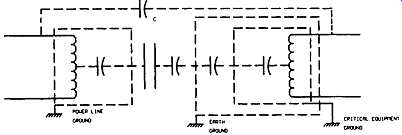
FIG. 15 Isolation transformer with two box shield
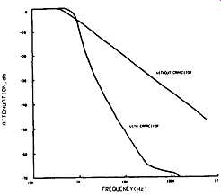
FIG. 16 Transverse mode attenuation curve
3.4 Line Conditioners
Line conditioners, also known as power line conditioners, provide multiple types of protection in one device. These systems offer characteristics of two or more enhancement devices and usually cost less than the combination of the individual power enhancers. For example, a TVSS and an isolation transformer with electronic tap changer may be considered as a power conditioner in practice.
The most common power conditioner is the ferroresonant regulator. These are designed to resonate with a suitable capacitor and the stored energy within the resonating system (system inductance and capacitor) provides some back-up for momentary outages, usually less than a fraction of a cycle to few cycles of the AC line. However low efficiency, high weight and volume of these "ferros" do promote considering other types of power conditioners.
4 Power Synthesis Equipment
Power synthesis equipment uses the incoming power as merely an energy source, creating "new power" for the critical load, which is completely isolated from the incoming waveform. Common types are stand by power sources (SPS), motor generators (MG) and uninterruptible power supplies (UPS). The next section details these systems.