AMAZON multi-meters discounts AMAZON oscilloscope discounts
- Introduction
- DC to DC Conversion Fundamentals
- Converter Topologies
- Control of DC to DC Converters
- Resonant Converters
- Special DC to DC Converter Designs
- DC to DC Converter Applications and ICs
- State of the Art and Future Directions
- References
1 Introduction
The linear power supply is a mature technology, having been used since the dawn of electronics. However, due to its low efficiency, the use of bulky heat sinks, cooling fans, and isolation transformers, this type of power supply tends to be unfit for most of today's compact electronic systems.
The disadvantages of linear power supplies are greatly reduced by the regulated switching power supply. In this technology, the AC line voltage is directly rectified and filtered to produce a raw high-voltage DC. This, in turn, is fed into a switching element which operates at a high frequency of 20 kHz to 1 MHz, chopping the DC voltage into a square wave. This high-frequency square wave is fed into the power isolation transformer, stepped down to a predetermined value and then rectified and filtered to produce the required DC output. This DC to DC conversion process which is at the heart of switching power supplies is examined in this section.
Switch mode power supplies have existed since the 1960s. Until the late 1970s, the task of efficiently converting one DC voltage to another using switching techniques was done with discrete components. Early systems were running at very low frequencies, usually between a few kHz to about 20 KHz, and were justified only for use in high power applications, usually above 500 watts.
The first ICs for switching power conversion were introduced in the late 1970s. During the mid 80s, switching techniques were introduced for much lower power ratings, while the operating frequency extended up to about 100 kHz.
Additional enhancements such as multiple output rails also became available.
Today, most switchers operate well above 500 kHz, with new magnetics, resonant techniques and surface mount technology extending this to several MHz. However, a major concern in such high-frequency switching power supplies is the minimization of the RFI pollution generated.
The recent rapid advancement of microelectronics has created a necessity for the development of sophisticated, efficient, lightweight power supplies which have a high power-to-volume (W/in 3) ratio, with no compromise in performance. High frequency switching power supplies, being able to meet these demands, have become the prime power source in a majority of modem electronic systems.
The combination of high efficiency (i.e., no large heat sinks) and relatively small magnetics, results in compact, light weight power supplies, with power densities in excess of 100 W/in 3 (Maliniak 1995 and Travis 1996) versus 0.3 W/in 3 for linear regulators. Still further innovations in DC/DC conversion are spurred by the proliferation of portable battery operated electronic devices and progressively plummeting logic voltages.
This section begins with a description of the basic principles of DC to DC conversion, and continues through more advanced resonant techniques to the latest technological innovations such as synchronous conversion and switched capacitor techniques. State of the art components are described as illustrative examples.
2 DC to DC Conversion Fundamentals
This section presents a brief overview of the DC to DC converter fundamentals, and a simplified analysis for characterizing the input/output relationship. More detailed descriptions can be found in (Brown 1990) and (Brown 1994). Ideal components are assumed for simplicity of analysis and description.
2.1 Modes of Operation
There are two major operational modes of the DC to DC converter within switching power supplies. They are the forward mode and the flyback mode.
Although they have only subtle differences between them with respect to component arrangement, their operation is significantly different, and each has advantages in certain areas of application.
2.1.1 Forward Mode Converters
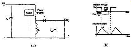
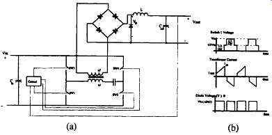
Fig. 1 (a) shows a simple forward mode converter. This type of converter can be recognized by an L-C filter section directly after the power switch or after the output rectifier on the secondary of a transformer. The Power Switch is a power transistor or a power MOSFET operated between fully-conduction and cut-off modes.
The operation of the converter can be seen by breaking its operation into two periods:
• Power Switch ON period: When the power switch is on, the input voltage is presented to the input of the L-C section, and the inductor current ramps upwards linearly. During this period the inductor stores energy.
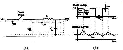
Above: Fig. 1 The forward mode converter (a) The basic circuit (b) Associated
waveforms
• Power Switch OFF period: When the power switch is off, the voltage at the input of the inductor flies below ground since the inductor current cannot change instantly. Then the diode becomes forward biased. This continues to conduct the current that was formally flowing through the power switch. During this period, the energy that was stored in the inductor is dumped on to the load. The current waveform through the inductor during this period is a negative linear ramp. The voltage and current waveforms for this converter are shown in Fig. l(b). The DC output load current value falls between the minimum and the maximum current values, and is controlled by the duty cycle. In typical applications, the peak inductor current is about 150 percent of the load current and the minimum is about 50 percent.
The advantages of forward mode converters are that they exhibit lower output peak-to-peak tipple voltages, and that they can provide high levels of output power, up to kilowatts.
2.1.2 Flyback Mode Converters
In this mode of operation, the inductor is placed between the input source and the power switch as shown in Fig. 2. This circuit is also examined in two stages:
• Power Switch ON period: During this period, a current loop including the inductor, the power switch and the input source is formed. The inductor current is a positive ramp and energy is stored in the inductor's core.
• Power Switch OFF period: When the power switch turns off, the inductor's voltage flies back above the input voltage, resulting in forward biasing the diode. The inductor voltage is then clamped at the output voltage. This voltage which is higher than the input voltage is called the flyback voltage.
The inductor current during this period is a negative ramp.
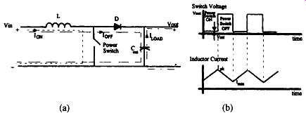
Above: Fig. 2 The flyback mode converter (a) The basic circuit (b) Associated
waveforms
In Fig. 2, the inductor current does not reach zero during the flyback period. This type of a flyback converter is said to operate in the continuous mode.
The core's flux is not completely emptied during the flyback period, and a residual amount of energy remains in the core at the end of the cycle. Accordingly, there may be instability problems in this mode. Therefore, the discontinuous mode is the preferred mode of operation in flyback mode converters. The voltage and current waveforms are shown in Fig. 3.
The only storage for the load in the flyback mode of operation is the output capacitor. This makes the output ripple voltage higher than in forward mode converters. The power output is lower than forward mode converters owing to higher peak currents that are generated when the inductor voltage flies back. As they consist of the fewest number of components, they are popular in low-to-medium power applications.
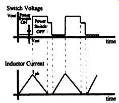
Above: Fig. 3 Voltage and current waveforms for the discontinuous flyback
mode converter
2.2 Analysis of DC to DC Converters
2.2.1 The Volt-Second Balance for Inductors
The input-output characteristics of all DC/DC converters can be examined by using the requirement that the initial and the final inductor current within a cycle should be the same for steady-state operation (i.e., the fact that the net energy storage within one switching cycle in each inductor should be zero).This leads to the volt-sec balance for the inductor, which means that the average voltage per cycle across the inductor must be zero, i.e., that the volt-sec products for the inductor during each switching cycle should sum to zero (Brown 1990) and (Bose 1992). This can be illustrated using a typical inductor current waveform as shown in Fig. 4.
Let the positive slope of the current be m I and the negative slope m^2.
For the initial and final currents to be the same:
Since the voltage across an inductor L is given by L di/dt,
Equation (3.2) can be written as a function of the duty cycle D
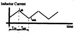
Above: Fig. 4 A typical inductor current waveform
Combining (3.1d) and (3.1e), where VLON and VLOFF are the voltages across the inductor during the switch ON and the OFF periods respectively and D is the duty cycle.
The output voltage of forward mode converters is given approximately by V_out = DV_in ' where D is the duty cycle of the switching waveform. Thus, this mode of operation always performs a step-down operation.
The output voltage for the flyback mode of operation is given by V_out = V_in/ (l-D). Thus, flyback mode converters are always used as step-up converters.
3 Converter Topologies
The converter topology refers to the arrangement of components within the converter. Converter topologies fall into two main categories: transformer-isolated and non-transformer-isolated. In each category, there are several topologies, with some available in both forms. An excellent discussion on converter topologies is found in (Bose 1992).
3.1 Non-Transformer-Isolated Converter Topologies
This type of switching converters are used when some external component such as a 50-60 Hz transformer or bulk power supply provides the DC isolation and protection. These are simple, thus easy to understand and design. However, they are more prone to failure due to lack of DC isolation. Hence these are used by designers mostly in situations such as distributed power systems, where a bulk power supply provides the necessary DC isolation.
There are four basic non-transformer-isolated topologies, the Buck (or stepdown), the Boost (or step-up), the Buck-Boost (or inverting), and the Cuk converters.
The Buck Converter
This is the most elementary forward-mode converter, and is the building block for all forward-mode topologies. The buck converter topology is shown in Fig. 5.
Applying equation (3. l f) to Fig. 5, we see that for steady-state operation: Hence,
As V_out < V_in this is called the Buck or the step-down converter.
Though the buck converter is capable of delivering over 1 kW in normal operation, it’s not a popular choice among experienced designers due to the following limitations:
Above: Fig. 5 The buck converter topology (a) The basic circuit (b) Associated waveforms
i. The input voltage must always be 1 to 2 V higher than the output in order to maintain regulation. This is similar to the headroom voltage requirement in linear regulators. The headroom voltage is the actual voltage drop between the input voltage and the output voltage during operation.
Ninety-five percent of all the power lost within the linear regulator is lost across this voltage drop.
ii. The finite reverse recovery time of the diode presents an instantaneous short circuit across the input source when the power switch turns on.
This adds stress to the power switch and the diode.
iii. If the semiconductor power switch fails in the short-circuited condition (which is a common mode of failure for such devices when they do fail), the input is short-circuited to the load. Additional means of protection must be provided to prevent this as discussed in (Brown 1990). The Boost Converter
The boost converter topology is shown in Fig. 6. This is an elementary flyback-mode converter as can be seen by comparing Fig. 2 with Fig. 6.
This circuit can also be analyzed using equation (3.1f) which gives:
As V_out > V_in this is called the boost or the step-up converter.
The power output of the boost topology is limited to about 150 W due to the high peak currents which stress the power switch and the diode. The ability of the boost regulator to prevent hazardous transients from reaching the load is also quite poor. Due to these reasons, many designers favor the flyback topology which is a transformer-isolated version of this converter. The flyback topology is discussed in Section 2.1.
The Buck-Boost Converter
The buck-boost converter topology is shown in Fig. 7. This is a fly back mode converter whose operation is very similar to that of the Boost topology. The difference between the two is that the positions of the inductor and the power switch have been reversed.
The inductor stores energy during the power switch's ON time and releases energy below ground through the diode into the output capacitor. This results in a negative voltage whose level is regulated by the duty cycle of the power switch.
Analyzing this circuit using equation (3.1f) gives,
From equation (3.4) it can be observed that, IV out l < V_in if D < 50% and IV out l > V i n if D > 50%. Hence this is called the buck-boost converter. Since the output voltage is opposite in polarity to the input, it’s also referred to as the inverting topology. However, due to the practical constraint of emptying the core's storage energy during the switch's OFF period, the duty cycle is limited to below 50% in most cases. The buck-boost topology also suffers from failure modes similar to those of the buck and the boost topologies (Brown 1990).
Above: Fig. 7 The buck-boost converter topology (a) The basic circuit
(b) Associated waveforms
The Cuk Converter
The Cuk converter reduces the switching component of the input and the output currents, and hence the ripple to a great extent. This is done by having an inductor in series with both the input and the output for either switch position. The Cuk converter is shown in Fig. 8.
When the power switch is OFF, the diode is ON and the capacitor charges with the current 11 OFF. The current 12 OFF FLOWS through the load and the diode.
When the power switch turns ON, the diode becomes reverse biased due to the capacitor voltage. The energy stored in the capacitor is dumped into the load through 12 ON. As the load current is allowed to flow continuously during either clock cycle, by suitable coupling of input and output inductors, the tipple in the input and output currents is very small. This can be nulled to zero by coupled inductor techniques as shown in (). The Cuk converter is based on capacitive energy transfer, unlike the other topologies, where inductors are used for energy transfer. The analysis of this topology is done by applying equation (3.1) to the two inductors in the circuit separately.
For inductor L 1 For inductor L 2 ...converter is buck-boost with polarity reversal.
The Cuk converter is closer to the ideal power supply compared to the other topologies. Therefore it has been referred to as an optimum switching power supply configuration, as it incorporates the advantages of switching technology and substantially eliminates the technology's main disadvantage, the switching currents.
Also, the Cuk converter can be implemented in transformer-isolated forms as well, as discussed in Section 2.2.6. A detailed description and analysis of the Cuk converter is found in (References).
3.2 Transformer-Isolated Converter Topologies
In non-transformer-isolated converter topologies, only semiconductors provide DC isolation from input to output. The transformer-isolated switching converter category relies on a physical barrier to provide galvanic isolation. Not only can this withstand very high voltages before failure, but it also provides a second form of protection in the event of a semiconductor failure. Another advantage is the ease of adding multiple outputs to the power supply without separate regulators for each. These features make transformer isolated topologies, the preferred ones by designers.
In the transformer-isolated category, there are both forward and flyback mode converter topologies. The isolation transformer now provides a step-up or step- down function. The topologies are called isolated forward, flyback, push-pull, half-bridge and full-bridge.
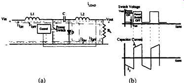
Above: Fig. 8 The Cuk converter topology (a) The basic circuit (b) Associated
waveforms
Above: Fig. 9 The Flyback Converter Topology (a) The basic circuit (b)
Associated waveforms
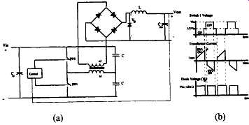
3.2.1 The Flyback Converter
The flyback converter topology and its waveforms are shown in Fig. 9.
This is the only flyback-mode converter in the transformer-isolated family of regulators. The flyback topology closely resembles the boost topology except for the addition of a secondary winding on the inductor. This flyback transformer is designed to perform the dual function of transformer and inductor.
During the power switch's on time, the full input is applied across the primary winding of the transformer, and the current flowing through it increases linearly.
When the power switch turns off, the output diode starts to conduct, passing the energy stored within the core material to the capacitor and the load. During this flyback period, the secondary current is a negative ramp. The flyback topology can operate in either the discontinuous mode or the continuous mode.
Because of the flyback converter's unipolar use of the transformer core's BH characteristics, the transformer core could get saturated. In such a condition, the power switch could fail due to the lowering of the primary inductance, and the resulting high primary current. The core should be designed to avoid this condition as described in (Brown 1990).
3.2.2 The Push-Pull Converter
The push-pull is a double ended topology (i.e., two power switches share the switching function). This forward-mode converter is shown in Fig. 10. It has similarities to the buck converter.
The input is applied to the center-tap of the primary of the transformer, and two power switches are connected across each section of the primary winding. The secondary voltage is full-wave rectified and applied to a buck-style LC section.
The two switches share the switching function by alternately turning on and off. When each switch turns on, current flows through its side of the primary.
Simultaneously, one half of the center-tapped secondary begins to conduct, forward biasing its respective diode, and letting the current into the load. Unlike in the flyback topology, the transformer does not store energy, but output current is drawn when either switch is on.
As the current flows in opposite directions in the primary winding during each switch's on period, the core material is driven in both the positive and the negative flux polarities. This reduces the possibility of core saturation, and also allows reduction of the core size by using it more efficiently. Another advantage is that this topology can provide twice the output power of a topology using one power switch operating at the same frequency. This feature enables the push-pull topology to generate output powers of several hundred watts.
For correct operation of this converter, there must be a dead time where neither transistor is conducting, to allow for the finite time necessary for the power switches to turn off (around 2 ItS for bipolar transistors and 50--400 nS for MOSFETs). If both the switches are allowed to conduct at the same time, a short circuit will be formed in the transformer, resulting in high levels of current which could destroy the power switches.
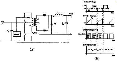
Above: Fig. 10 The push-pull converter topology (a) The basic circuit
(b) Associated waveforms.
This topology however, suffers from one serious flaw, as neither the two halves of the winding nor the two power switches can be absolutely identical due to real-world factors. Any asymmetry will eventually lead to saturation of one side of the transformer and to the destruction of the corresponding power switch. Some methods of overcoming this core imbalance are discussed in (Brown 1990). The topologies discussed in the remainder of this section eliminate this problem.
3.2.3 The Half-Bridge Converter
The half-bridge topology is also double ended. However, the half-bridge topology has only one primary winding which is connected between a pull-up/pull-down configuration of power switches and the centre node between two series capacitors as shown in Fig. 11.
The capacitor centre node voltage is fixed approximately at half the input voltage. The other end of the primary is alternately presented with the input voltage and ground by the two power switches. Therefore, only half the input voltage appears across the primary winding at any time.
The switches alternate as before, and the direction of current alternates with each conducting switch. Hence the transformer core is operated in a bipolar fashion.
This topology exhibits a self-core balancing ability, which is accomplished by the capacitors. The centre node voltage will adjust itself according to the direction of higher flux density within the transformer. This reduces the voltage across the primary in the direction of impending saturation.
Since only half the input voltage appears across the primary, the peak current in the half-bridge topology is twice as high as in the push-pull topology with identical power output. Thus, this topology is not suited for as high power applications as the push-pull topology.
Above: Fig. 11 The half-bridge converter topology (a) The basic
circuit (b) Associated waveforms.
3.2.4 The Full-Bridge Converter
This is also a double ended topology. Its power output is significantly higher than that of the half-bridge topology. This is because the balancing capacitors are replaced with another pair of switches, identical to the first pair. This converter is shown in Fig. 12.
Two of the four power switches are turned on simultaneously during each conduction cycle (e.g., SW1 and SW4 or SW2 and SW3). This places the full input voltage across the primary winding, which reduces the peak currents flowing through it compared to the half-bridge topology.
This effectively doubles the power handling capacity of this topology over the half-bridge. Therefore this is used in applications requiring output powers of 300 W to several kilowatts.
Core balancing may be achieved in this topology by placing a small, non-polarized capacitor in series with the primary winding (Brown 1990). The average DC voltage across this capacitor causes to bring the core away from saturation. Core balancing is essential in this topology, as core saturation would lead to instant destruction of semiconductors at the power levels at which they operate.
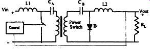
3.2.5 The Transformer-Isolated Cuk Converter
The transformer-isolated version of the Cuk converter is shown in Figure 313. Comparing this with the basic Cuk converter in Fig. 8 it’s seen that DC isolation is achieved at the expense of one additional capacitor besides the isolation transformer.
The same charge balance of the non-isolated version is valid for capacitors C A and C B. Thus, average currents in both transformer windings are zero. This is unlike the flyback topology shown in Fig. 9 where a large DC bias current is carded by the transformers. Therefore the transformer in the Cuk converter has advantages in terms of compactness and leakage reactances. As this circuit retains all the properties of the basic Cuk converter, the zero ripple extension using coupled inductor technique can be applied to this also as described in (References).
Above: Fig. 12 The full-bridge converter topology (a) The basic circuit
(b) Associated waveforms.
Above: Fig. 13 The transformer-isolated cuk converter topology
TABLE 1 Comparison of Converter Topologies
Topology:
Buck Boost Buck-boost Flyback Push-pull Half-bridge Full-bridge
V_in /Vout:
I/( I-D)
-D/(I-D) N2D/NI(ID) 2~2Dm1 N2D/N 1 2N2D/N 1
Advantages:
High efficiency, simple, low switch stress, low ripple High efficiency, simple, low input ripple current Voltage inversion without a transformer, simple, high frequency operation Isolation, low parts count, has no secondary output inductors Isolation, good transformer utilization, good at low input voltages, low output ripple Isolation, good transformer utilization, switches rated at the input voltage, low output ripple Isolation, good transformer utilization, switches rated at the input voltage, low output ripple
Disadvantages:
No isolation, potential over-voltage if switch shorts No isolation, high switch peak current, regulator loop hard to stabilize, high output ripple, unable to control short circuit current
.... No isolation, regulator loop hard to stabilize, high output ripple Poor transformer utilization, high output ripple, fast recovery diode required , Cross conduction of switches possible, high parts count, transformer design critical, high voltage required for switches
..... Poor transient response, high parts count, cross conduction of the switches possible High parts count, cross conduction of switches possible Typical Application Environment Small sized imbedded systems ,, Power-factor correction, battery upconverters Inverse output voltages Low output power, multiple output Low output voltage High input voltage, moderate to high power High power, high input voltage
V_in(dc) Range :V)
5-1000 5-600 5-600 5 - 500 501000 501000 501000
Typical Efficiency (%)
78 80 80 80 75 75 73
Relative Parts Cost
1.0 1.0 1.0 1.2 2.0
2.2 2.5
============
3.3 Summary and Comparison of Converter Topologies
The converter topology has a major bearing on the conditions in which the power supply can operate safely, and on the amount of power it can deliver. Cost vs. performance trade-offs are also needed in selecting a suitable converter topology for an application.
The primary factors that determine a choice of topology are whether DC isolation is needed, the peak currents and voltages that the power switches are subjected to, the voltages applied to transformer primaries, the cost and the reliability.
Some relative merits of the converter topologies as well as their advantages, disadvantages and typical applications are summarized in Table 3-1. Mathematical expressions for estimating some of the important parameters such as peak currents and voltages, output power etc. are found in (Brown 1990) and (Brown 1994). A comparison of the strengths and weaknesses of the different converter topologies are also discussed in ( Moore 1994).
The industry has settled into several primary topologies for a majority of the applications. Due to reasons discussed in Section 3.3.2, transformer-isolated topologies have become more popular than non-transformer-isolated topologies.
Fig. 14 illustrates the approximate range of usage for these topologies.
The boundaries to these areas are determined primarily by the amount of stress the power switches must endure and still provide reliable performance. The boundaries delineated in Fig. 14 represent approximately 20A of peak current.
The flyback configuration is used predominantly for low to medium output power (150W) applications because of its simplicity and low cost. Unfortunately, the flyback topology exhibits much higher peak currents than do the forward-mode supplies. Therefore, at higher output powers, it quickly becomes an unsuitable choice. For medium-power applications (100 to 400 W) the half-bridge topology becomes the predominant choice. The half-bridge is more complex than the flyback and therefore costs more.
However, its peak currents are about one-third to one-half of those exhibited by the flyback. Above 400 W the dominant topology is the full-bridge, which offers the most effective utilization of the full capacity of the input power source. It’s also the most expensive to build, but for those power levels the additional cost becomes a trivial matter. Above 150 W the push-pull topology is also sometimes used.
However, this exhibits some shortcomings such as core imbalance, that may make it tricky to use (Brown 1990). Estimating the major power supply parameters at the beginning of the design and by using charts such as Fig. 14 will lead to the selection of a final topology which is safe, reliable and cost-effective.
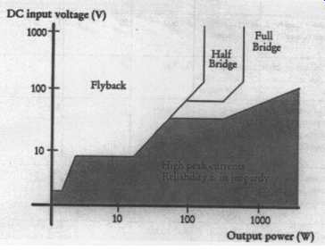
Above: Fig. 14 Industry favorite configurations and their areas of usage
4 Control of DC to DC Converters
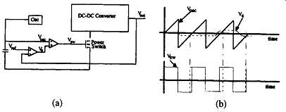
In a PWM switch mode power supply, a square wave pulse is normally generated by the control circuit to drive the switching transistor ON and OFF. By varying the width of the pulse, the conduction time of the transistor is correspondingly varied, thus regulating the output voltage. The major function of the control subsection of a PWM supply is thus to sense any change in the DC output voltage and adjust the duty cycle of the power switches to correct for such changes.
An oscillator sets the basic frequency of operation of the power supply. A stable, temperature-compensated reference is used to which the output voltage is compared in a high-gain voltage error amplifier. An error-voltage to pulse width converter is used to adjust the duty cycle.
The PWM control circuit may be single ended for driving single-transistor converters such as the buck or boost topologies, or it may be double ended to drive multiple-transistor converters such as the push-pull or half-bridge topologies.
There are two basic modes of control used in PWM converters: voltage mode and current mode. Variable frequency control techniques used mostly in resonant power supplies are discussed in a subsequent section.
4.1 PWM Control Techniques
4.1.1 Voltage-Mode Control
Above: Fig. 15 Voltage-mode control (a) Block diagram (b) Associated
waveforms
This is the traditional mode of control in PWM switching converters. It’s also called single-loop control as only the output is sensed and used in the control circuit.
A simplified diagram of a voltage-mode control circuit is shown in Fig. 15.
The main components of this circuit are an oscillator, an error amplifier, and a comparator. The output voltage is sensed and compared to a reference. The error voltage is amplified in a high-gain amplifier. This is followed by a comparator which compares the amplified error signal with a saw-tooth waveform generated across a timing capacitor.
The comparator output is a pulse-width modulated signal which serves to correct any drift in the output voltage. As the error signal increases in the positive direction, the duty cycle is decreased, and as the error signal increases in the negative direction, the duty cycle is increased.
The voltage mode control technique works well when the loads are constant.
If the load or the input changes quickly, the delayed response of the output poses a drawback to the control circuit as it only senses the output voltage. Also, the control circuit cannot protect against instantaneous overcurrent conditions on the power switch. These drawbacks are overcome in current-mode control.
Above: Fig. 16 Current mode control (a) Block diagram (b) Associated
waveforms
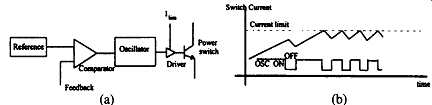
4.1.2 Current-Mode Control
This is a multiloop control technique, which has an AC current feedback loop in addition to the voltage feedback loop. This second loop directly controls the peak inductor current with the error signal rather than controlling the duty cycle of the switching waveform. Fig. 16 shows a block diagram of a basic current-mode control circuit.
The error amplifier compares the output to a fixed reference. The resulting error signal is then compared with a feedback signal representing the switch current in the current sense comparator. This comparator output resets a flip flop which is set by the oscillator. Therefore, switch conduction is initiated by the oscillator and terminated when the peak inductor current reaches the threshold level established by the error amplifier output.
Thus the error signal controls the peak inductor current on a cycle-by-cycle basis. The level of the error voltage dictates the maximum level of peak switch current. If the load increases, the voltage error amplifier allows higher peak currents.
The inductor current is sensed through a ground-referenced sense resistor in series with the switch.
The disadvantages of this mode of control are loop instability above 50% duty cycle, less than ideal loop response due to peak instead of average current sensing, tendency towards subharmonic oscillation and noise sensitivity, particularly at very small ripple current.
However, with careful design as explained in (Brown 1990), etc., these disadvantages can be overcome. Therefore, current-mode control becomes an attractive option for high frequency switching power supplies.
The comparator compares the feedback pin voltage with the reference signal.
When the feedback voltage drops below the reference, the comparator switches on the oscillator. The driver amplifier boosts the signal level to drive the output power switch.
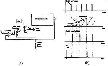
4.1.3 Gated Oscillator Control
Conventional PWM control techniques are fixed-frequency variable-pulse-width techniques. However, a new method of control for PWM converters is the gated oscillator method which turns the oscillator on with fixed pulse widths and turns it off using an overcurrent condition. The off-time is used to control the output. Fig. 17 shows a block diagram of this control method.
The switch cycling action raises the output voltage and hence the feedback voltage. When the feedback voltage rises above the reference, the oscillator is gated off. The limit input sets the maximum switch current. When the maximum limit is exceeded, the switch is turned off.
The switch current is generally detected by sampling a small fraction of it and passing it through a resistor. Since the switch is cycled only when the feedback voltage drops below the reference voltage, this type of architecture has a very low supply current, and hence is suitable only for very low power applications (Brown 1994), (Linear Technology Corp. 1992).
Above: Fig. 17 Gated oscillator control (a) Block diagram (b) Associated
waveforms
4.2 Control Integrated Circuits
A wide variety of ICs have been developed to implement the control functions in switching power supplies. In addition to the basic functions of control circuits described above, these ICs provide more advanced functions and facilities such as:
(i) Overcurrent protection.
(ii) Soft-start facilities that start the power supply in a smooth fashion, reducing the inrush current.
(iii) Dead-time control which fixes the maximum pulse width, to prevent the simultaneous conduction of two power switches.
(iv) Undervoltage lockout to prevent the supply from starting when there is insufficient voltage within the control circuit for driving the power switches to saturation.
Selection of a control IC for a particular application depends on the power switch type, the intended topology, and the control mode as well as on the required output power, peak currents, and voltages. Another important factor is whether the power transistor is integrated on the control IC die itself.
Popular switching power supply control ICs, their features and applications are described in (Maliniak 1995), (Brown 1990), (Brown 1994), and (Linear Technology Corp. 1990).
4.2.1 A Typical Voltage-Mode Controller
Fig. 18 shows the functional block diagram of the TIA94 voltage mode controller from Motorola Inc. (Motorola, Inc., 1997). Control for both push-pull and single-ended operation can be achieved with this chip. The frequency of the oscillator is set by the external resistors R T and C T. The typical operating frequency is 40 kHz, and the maximum is 200 kHz.
Output pulse width modulation is accomplished by comparison of the positive sawtooth waveform across the capacitor to either of two control signals. The NOR gates, which drive the output transistors are enabled only when the flip-flop clock input is in its low state. This happens only during that portion of time when the sawtooth voltage is greater than the control signals. Therefore, an increase in control signal amplitude causes a corresponding linear decrease of output pulse width.
4.2.2 A Typical Current-Mode Controller
Fig. 19 shows the functional block diagram of the MAX747 current mode controller from Maxim Integrated Circuits (Maxim Integrated Products 1994). This is a CMOS step-down controller, which drives external P-channel FETs.
This IC operates in continuous mode under heavy loads, but in discontinuous mode at light loads.
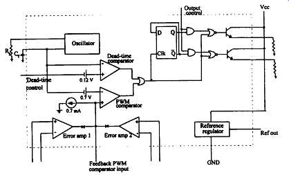
Above: Fig. 18 The functional block diagram of the TL 494 Voltage Mode
Controller IC (Copyright of Motorola, used by permission)
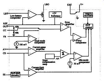
Above: Fig. 19 The functional block diagram of the MAX747 Current-Mode
Controller IC (Maxim Integrated Products)
Stability of the inner current-feedback loop is provided by a slope-compensation scheme that adds a ramp signal to the current-sense amplifier output. The switching frequency is nominally 100 kHz and the duty cycle varies from 5 percent to 96 percent depending on the input/output voltage ratio. EXT provides the gate drive for the external FET.