AMAZON multi-meters discounts AMAZON oscilloscope discounts
4. Bipolar Power Transistors
During the last two decades, attention has been focused on high power transistors as switching devices in inverters, SMPS and similar switching applications.
New devices with faster switching speeds and lower switching losses are being developed that offer performance beyond that of thyristors. With their faster speed, they can be used in an inverter circuit operating at frequencies over 200 KHz. In addition, these devices can be readily turned off with a low-cost reverse base drive without the costly commutation circuits required by thyristors.
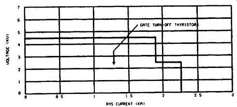
FIG. 15 Ratings covered by available GTOs (Reproduced by permission of
GEC Plessey Semiconductors, UK)
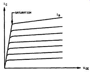
FIG. 16 Typical output characteristics of BJT
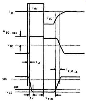
FIG. 17 Bipolar transistor switching waveforms
4.1 Bipolar Transistor as a Switch
The bipolar transistor is essentially a current-driven device. That is, by injecting a current into the base terminal a flow of current is produced in the collector.
There are essentially two modes of operation in a bipolar transistor: the linear and saturating modes. The linear mode is used when amplification is needed, while the saturating mode is used to switch the transistor either on or off.
FIG. 16 shows the V-I characteristic of a typical bipolar transistor. Close examination of these curves shows that the saturation region of the V-I curve is of interest when the transistor is used in a switching mode. At that region a certain base current can switch the transistor on, allowing a large amount of collector current to flow, while the collector-to-emitter voltage remains relatively small.
In actual switching applications a base drive current is needed to turn the transistor on, while a base current of reverse polarity is needed to switch the transistor back off. In practical switching operations certain delays and storage times are associated with transistors. In the following section are some parameter definitions for a discrete bipolar transistor driven by a step function into a resistive load.
FIG. 17 illustrates the base-to-emitter and collector-to-emitter waveforms of a bipolar NPN transistor driven into a resistive load by a base current pulse 1B. The following are the definitions associated with these waveforms:
Delay Time, td
Delay time is defined as the interval of time from the application of the base drive current IBI to the point at which the collector-emitter voltage VCE has dropped to 90 percent of its initial off value.
Rise Time, t r
Rise time is defined as the interval of time it takes the collector-emitter voltage VCE to drop to 10 percent from its 90 percent off value.
Storage Time, tstg
Storage time is the interval of time from the moment reverse base drive IB2 is applied to the point where the collector-emitter voltage VCE has reached 10 percent of its final off value.
Fall Time, tf,VCE
Fall time is the time interval required for the collector-emitter voltage to increase from 10 to 90 percent of its off value.
4.2 Inductive Load Switching
In the previous section, the definitions for the switching times of the bipolar transistor were made in terms of collector-emitter voltage. Since the load was defined to be a resistive one, the same definitions hold true for the collector current.
However, when the transistor drives an inductive load, the collector voltage and current waveforms will differ. Since current through an inductor does not flow instantaneously with applied voltage, during turn-off, one expects to see the collector-emitter voltage of a transistor rise to the supply voltage before the current begins to fall. Thus, two fall time components may be defined, one for the collector-emitter voltage tf, vc E, and the other for the collector current tf, ic FIG. 18 shows the actual waveforms.
Observing the waveforms we can define the collector-emitter fall time tf, vcE in the same manner as in the resistive case, while the collector fall time tf, lc may be defined as the interval in which collector current drops from 90 to 10 percent of its initial value. Normally, the load inductance L behaves as a current source, and therefore it charges the base-collector transition capacitance faster than the resistive load. Thus, for the same base and collector currents the collector-emitter voltage fall time tf, VCE is shorter for the inductive circuit.
4.3 Safe Operating Area and V-I Characteristics
The output characteristics (I C Versus VCE) of a typical npn power transistor are shown in FIG. 19(a). The various curves are distinguished from each other by the value of the base current.
Several features of the characteristics should be noted. First, there is a maximum collector-emitter voltage that can be sustained across the transistor when it is carrying substantial collector current. The voltage is usually labeled BVsu s. In the limit of zero base current, the maximum voltage between collector and emitter that can be sustained increases somewhat to a value labeled BVcE O, the collector-emitter breakdown voltage when the base is open circuited. This latter voltage is often used as the measure of the transistor's voltage standoff capability because usually the only time the transistor will see large voltages is when the base current is zero and the BJT is in cutoff.
The voltage BVCBO is the collector-base breakdown voltage when the emitter is open circuited. The fact that this voltage is larger than BVCEO is used to advantage in so-called open-emitter transistor turn-off circuits.
The region labeled primary breakdown is due to conventional avalanche breakdown of the collector-base junction and the attendant large flow of current.
This region of the characteristics is to be avoided because of the large power dissipation that clearly accompanies such breakdown.
The region labeled second breakdown must also be avoided because large power dissipation also accompanies it, particularly at localized sites within the semiconductor. The origin of second breakdown is different from that of avalanche breakdown and will be considered in detail later in this section. BJT failure is often associated with second breakdown.
The major observable difference between the I-V characteristics of a power transistor and those of a logic level transistor is the region labeled quasi-saturation on the power transistor characteristics of FIG. 19(a). Quasi-saturation is a consequence of the lightly doped collector drift region found in the power transistor.
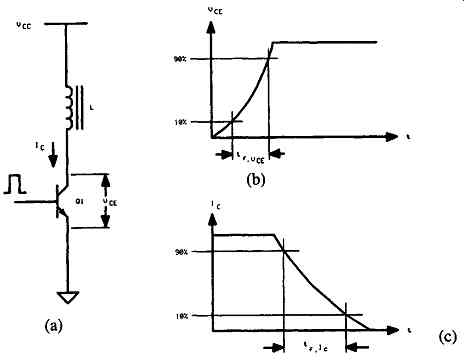
FIG. 18 A bipolar switching transistor driving an inductive load with
associated fall time waveforms (a) Circuit (b) Voltage waveform (c) Current
waveform
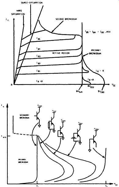
FIG. 19 Current-voltage characteristics of a NPN power transistor showing
breakdown phenomenon (a) indication of quasi saturation (b) relative primary
and secondary breakdown conditions for different bias levels.
Logic level transistors do not have this drift region and so do not exhibit quasi-saturation. Otherwise all of the major features of the power transistor characteristic are also found on those of logic level devices.
FIG. 19(b) indicates the relative magnitudes of npn transistor collector breakdown characteristics, showing primary and secondary breakdown with different base bias conditions. With low gain devices V a is close to V b in value, but with high gain devices V b may be 2 to 3 times that of V a. Notice that negative resistance characteristics occur after breakdown, as is the case with all the circuit-dependent breakdown characteristics. (B. W. Williams 1992) provides a detailed explanation on the behavior.
4.3.1 Forward-Bias Secondary Breakdown
In switching process BJTs are subjected to great stress, during both turn-on and turn-off. It is imperative that the engineer clearly understands how the power bipolar transistor behaves during forward and reverse bias periods in order to design reliable and trouble-free circuits.
The first problem is to avoid secondary breakdown of the switching transistor at turn-on, when the transistor is forward-biased. Normally the manufacturer's specifications will provide a safe-operating area (SOA) curve, such as the typical one shown in FIG. 20. In this figure collector current is plotted against collector emitter voltage. The curve locus represents the maximum limits at which the transistor may be operated. Load lines that fall within the pulsed forward-bias SOA curve during turn-on are considered safe, provided that the device thermal limitations and the SOA turn-on time are not exceeded.
The phenomenon of forward-biased secondary breakdown is caused by hot spots which are developed at random points over the working area of a power transistor, caused by unequal current conduction under high-voltage stress. Since the temperature coefficient of the base-to-emitter junction is negative, hot spots increase local current flow. More current means more power generation, which in turn raises the temperature of the hot spot even more.
Since the temperature coefficient of the collector-to-emitter breakdown voltage is also negative, the same rules apply. Thus is the voltage stress is not removed, ending the current flow, the collector-emitter junction breaks down and the transistor fails because of thermal runaway.
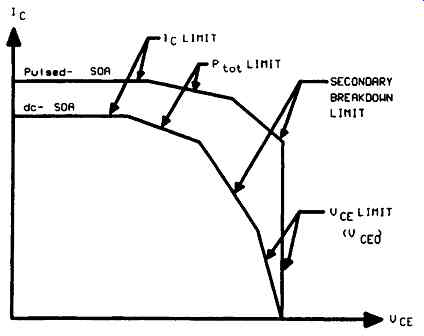
FIG. 20 DC and pulse SOA for BJT
4.3.2 Reverse-Bias Secondary Breakdown
It was mentioned in previous paragraphs that when a power transistor is used in switching applications, the storage time and switching losses are the two most important parameters with which the designer has to deal extensively.
On the other hand the switching losses must also be controlled since they affect the overall efficiency of the system. FIG. 21 shows turn-off characteristics of a high-voltage power transistor in resistive and inductive loads. Inspecting the curves we can see that the inductive load generates a much higher peak energy at turn-off than its resistive counterpart. It is then possible, under these conditions, to have a secondary breakdown failure if the reverse-bias safe operating area (RBSOA) is exceeded.
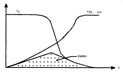
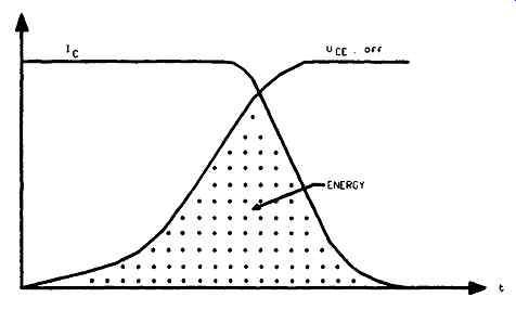
FIG. 21 Inductive load Turn-off characteristics of a high voltage BJT (a)
Resistive load (b)
The RBSOA curve ( FIG. 22) shows that for voltages below VCEO the safe area is independent of reverse-bias voltage VEB and is only limited by the device collector current IC. Above VCEO the collector current must be derated depending upon the applied reverse-bias voltage.
It is then apparent that the reverse-bias voltage VEB is of great importance and its effect on RBSOA very interesting. It is also important to remember that avalanching the base-emitter junction at turn-off must be avoided, since turn-off switching times may be decreased under such conditions. In any case, avalanching the base-emitter junction may not be considered relevant, since normally designers protect the switching transistors with either clamp diodes or snubber networks to avoid such encounters.
4.4 Darlington Transistors
The on-state voltage VCE(sat ) of the power transistors is usually in the 1-2 V range, so that the conduction power loss in the BJT is quite small. BJTs are current-controlled devices and base current must be supplied continuously to keep them in the on-state. The DC current gain hFE is usually only 5-10 in high-power transistors and so these devices are sometimes connected in a Darlington or triple Darlington configuration as is shown in FIG. 23 to achieve a larger current gain. However, some disadvantages accrue in this configuration including slightly higher overall VCE(sat ) values and slower switching speeds. The current gain of the pair hFE is
hFE = hFE1 x hFE2 + hFE l + hFE 2 (eqn. 4)
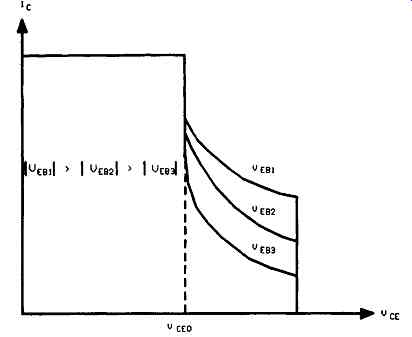
FIG. 22 RBSOA plot for a high voltage BJT as a function of reverse-bias
volt- age VEB.
Darlington configurations using discrete BJTs or several transistors on a single chip (a Monolithic Darlington (MD)) have significant storage time during the turn-off transition. Typical switching times are in the range of a few hundred nanoseconds to a few microseconds.
BJTs including MDs are available in voltage ratings up to 1400 V and current ratings of a few hundred amperes. In spite of a negative temperature coefficient of on-state resistance, modem BJTs fabricated with good quality control can be paralleled provided that care is taken in the circuit layout and that some extra current margin is provided.
FIG. 24 shows a practical Monolithic Darlington pair with diode D1 added to speed up the turn-off time of Q1 and D2 added for half and full bridge circuit applications. Resistors R1 and R2 are low value resistors and provide a leakage path for Q1 and Q2.
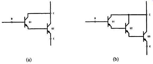
FIG. 23 Darlington configurations (a) Darlington (b) Triple darlington
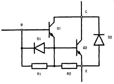
FIG. 24 A practical Monolithic Darlington pair
5. Power MOSFETs
5.1 Introduction
Compared to BJTs which are current controlled devices, field effect transistors are voltage controlled devices. There are two basic field-effect transistors (FETs): the junction FET (JFET) and the metal-oxide semiconductor FET (MOSFET). Both have played important roles in modem electronics. The JFET has found wide application in such cases as high-impedance transducers (scope probes, smoke detectors, etc.) and the MOSFET in an ever-expanding role in integrated circuits where CMOS (Complementary MOS) is perhaps the most well-known.
Power MOSFETs differ from bipolar transistors in operating principles, specifications, and performance. In fact, the performance characteristics of MOSFETS are generally superior to those of bipolar transistors: significantly faster switching time, simpler drive circuitry, the absence of a second-breakdown failure mechanism, the ability to be paralleled, and stable gain and response time over a wide temperature range. The MOSFET was developed out of the need for a power device that could work beyond the 20 KHz frequency spectrum, anywhere from 100 KHz to above 1 MHz, without experiencing the limitations of the bipolar power transistor.
5.2 General Characteristics
Bipolar transistors are described as minority-carrier devices in which injected minority carriers recombine with majority carders. A drawback of recombination is that it limits the device's operating speed. Current-driven base-emitter input of a bipolar transistor presents a low-impedance load to its driving circuit. In most power circuits, this low-impedance input requires somewhat complex drive circuitry.
By contrast, a power MOSFET is a voltage-driven device whose gate terminal is electrically isolated from its silicon body by a thin layer of silicon dioxide (SiO2). As a majority-carrier semiconductor, the MOSFET operates at much higher speed than its bipolar counterpart because there is no charge-storage mechanism.
A positive voltage applied to the gate of an n-type MOSFET creates an electric field in the channel region beneath the gate; that is, the electric charge on the gate causes the p-region beneath the gate to convert to an n-type region, as shown in FIG. 25(a).
This conversion, called the surface-inversion phenomenon, allows current to flow between the drain and source through an n-type material. In effect, the MOSFET ceases to be an n-p-n device when in this state. The region between the drain and source can be represented as a resistor, although it does not behave linearly, as a conventional resistor would. Because of this surface-inversion phenomenon, then, the operation of a MOSFET is entirely different from that of a bipolar transistor.
By virtue of its electrically-isolated gate, a MOSFET is described as a high input impedance, voltage-controlled device, compared to a bipolar transistor. As a majority-cartier semiconductor, a MOSFET stores no charge, and so can switch faster than a bipolar device. Majority-carrier semiconductors also tend to slow down as temperature increases. This effect brought about by another phenomenon called carder mobility makes a MOSFET more resistive at elevated temperatures, and much more immune to the thermal-runaway problem experienced by bipolar devices. Mobility is a term that defines the average velocity of a carrier in terms of the electrical field imposed on it.
A useful by-product of the MOSFET process is the internal parasitic diode formed between source and drain, FIG. 25(b). (There is no equivalent for this diode in a bipolar transistor other than in a bipolar Darlington transistor.) Its characteristics make it useful as a clamp diode in inductive-load switching.
Different manufacturers use different techniques for constructing a power FET, and names like HEXFET, VMOS, TMOS, etc., have become trademarks of specific companies.
5.3 MOSFET Structures and On Resistance
Most Power MOSFETs are manufactured using various proprietary processes by various manufactures on a single silicon chip structured with a large number of closely packed identical cells. For example, Harris Power MOSFETs are manufactured using a vertical double-diffused process, called VDMOS or simply DMOS. In these cases, a 120-mil 2 chip contains about 5,000 cells and a 240-mil 2 chip has more than 25,000 cells.
One of the aims of multiple-cells construction is to minimize the MOSFET parameter rDS(ON) when the device is in the on-state. When rDS(ON) is minimized, the device provides superior power-switching performance because the voltage drop from drain to source is also minimized for a given value of drain-source current.
Reference 6 provides more details.
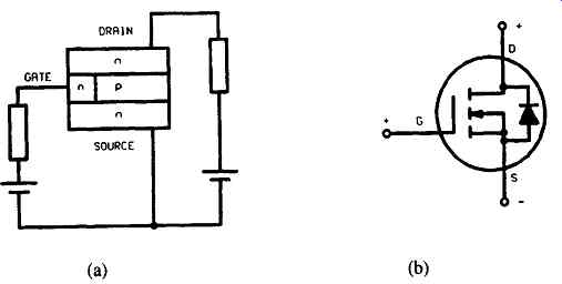
FIG. 25 Structure of N-channel MOSFET and symbol (a) Structure (b) Symbol
5.4 I-V Characteristics
FIG. 26 shows the drain-to-source operating characteristics of the power MOSFET. Although curve is similar to the case of bipolar power transistor ( FIG. 15), there are some fundamental differences.
The MOSFET output characteristic curves reveal two distinct operating regions, namely, a "constant resistance" and a "constant current." Thus, as the drainto-source voltage is increased, the drain current increases proportionally, until a certain drain-to-source voltage called "pinch off" is reached. After pinch off, an increase in drain-to-source voltage produces a constant drain current.
When the power MOSFET is used as a switch, the voltage drop between the drain and source terminals is proportional to the drain current; that is, the power MOSFET is working in the constant resistance region, and therefore it behaves essentially as a resistive element. Consequently the on-resistance RDS,o n of the power MOSFET is an important figure of merit because it determines the power loss for a given drain current, just as VCE,sat is of importance for the bipolar power transistor.
By examining FIG. 26, we note that the drain current does not increase appreciably when a gate-to-source voltage is applied; in fact, drain current starts to flow after a threshold gate voltage has been applied, in practice somewhere between 2 and 4V. Beyond the threshold voltage, the relationship between drain current and gate voltage is approximately equal. Thus, the transconductance gfs, which is defined as the rate of change of drain current to gate voltage, is practically constant at higher values of drain current. FIG. 27 illustrates the transfer characteristics of I D versus VDS, while FIG. 28 shows the relationship of transconductance gfs to drain current.
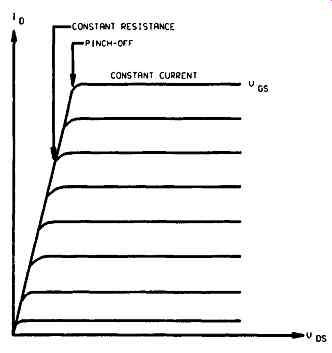
FIG. 26 Typical output characteristics of a MOSFET
It is now apparent that a rise in transconductance results in a proportional rise in the transistor gain, i.e., larger drain current flow, but unfortunately this condition swells the MOSFET input capacitance. Therefore, carefully designed gate drivers must be used to deliver the current required to charge the input capacitance in order to enhance the switching speed of the MOSFET.
5.5 Gate Drive Considerations
The MOSFET is a voltage controlled device; that is, a voltage of specified limits must be applied between gate and source in order to produce a current flow in the drain.
Since the gate terminal of the MOSFET is electrically isolated from the source by a silicon oxide layer, only a small leakage current flows from the applied voltage source into the gate. Thus, the MOSFET has an extremely high gain and high impedance.
In order to turn a MOSFET on, a gate-to-source voltage pulse is needed to deliver sufficient current to charge the input capacitor in the desired time. The MOSFET input capacitance Cis s is the sum of the capacitors formed by the metal-oxide gate structure, from gate to drain (CGD) and gate to source (CGs). Thus, the driving voltage source impedance Rg must be very low in order to achieve high transistor speeds. A way of estimating the approximate driving generator impedance, plus the required driving current, is given in the following equations:
Rg = t, (or t,)/2.2Ciss (eqn. 5)
and
Ig = Ciss dv/dt (eqn. 6)
Where Rg = generator impedance, Cis s = MOSFET input capacitance, pF dv/dt = generator voltage rate of change, V/ns To turn off the MOSFET, we need none of the elaborate reverse current generating circuits described for bipolar transistors. Since the MOSFET is a majority carder semiconductor, it begins to turn off immediately upon removal of the gateto-source voltage. Upon removal of the gate voltage the transistor shuts down, presenting a very high impedance between drain and source, thus inhibiting any current flow, except leakage currents (in microamperes).
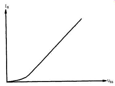
FIG. 27 Transfer characteristics of a power MOSFET
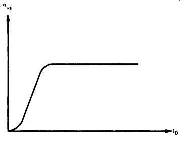
FIG. 28 Relationship of transconductance (gfs) to I D of a power MOSFET
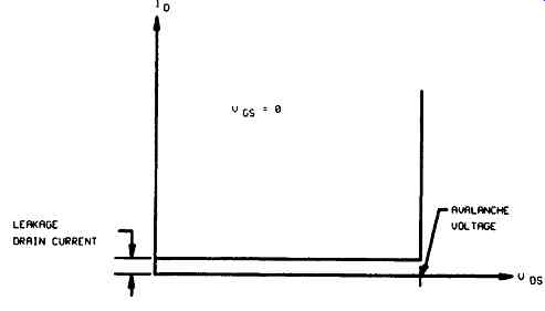
FIG. 29 Drain-to-source blocking characteristics of the MOSFET
FIG. 29 illustrates the relationship of drain current versus drain-to-source voltage. Note that drain current starts to flow only when the drain-to-source avalanche voltage is exceeded, while the gate-to-source voltage is kept at 0V.
5.6 Temperature Characteristics
The high operating temperatures of bipolar transistors are a frequent cause of failure. The high temperatures are caused by hot-spotting, the tendency of current in a bipolar device to concentrate in areas around the emitter. Unchecked, this hot spotting results in the mechanism of thermal runaway, and eventual destruction of the device. MOSFETs do not suffer this disadvantage because their current flow is in the form of majority carriers. The mobility of majority carders in silicon decreases with increasing temperature.
This inverse relationship dictates that the carders slow down as the chip gets hotter. In effect, the resistance of the silicon path is increased, which prevents the concentrations of current that lead to hot spots. In fact if hot spots do attempt to form in a MOSFET, the local resistance increases and defocuses or spreads out the current, rerouting it to cooler portions of the chip.
Because of the character of its current flow, a MOSFET has a positive temperature coefficient of resistance, as shown by the curves of FIG. 30. The positive temperature coefficient of resistance means that a MOSFET is inherently stable with temperature fluctuation, and provides its own protection against thermal runaway and second breakdown. Another benefit of this characteristic is that MOSFET can be operated in parallel without fear that one device will rob current from the others. If any device begins to overheat, its resistance will increase, and its current will be directed away to cooler chips.
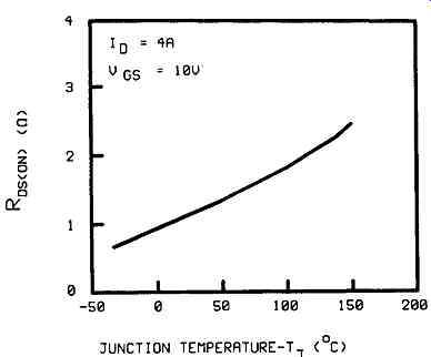
FIG. 30 Positive temperature coefficient of a MOSFET
5.7 Safe Operating Area
In the discussion of the bipolar power transistor, it was mentioned that in order to avoid secondary breakdown, the power dissipation of the device must be kept within the operating limits specified by the forward-bias SOA curve. Thus, at high collector voltages the power dissipation of the bipolar transistor is limited by its secondary breakdown to a very small percentage of full rated power. Even at very short switching periods the SOA capability is still restricted, and the use of snubber networks is incorporated to relieve transistor switching stress and avoid secondary breakdown.
In contrast, the MOSFET offers an exceptionally stable SOA, since it does not suffer from the effects of secondary breakdown during forward bias. Thus, both the DC and pulsed SOA are superior to that of the bipolar transistor. In fact with a power MOSFET it is quite possible to switch rated current at rated voltage without the need of snubber networks. Of course, during the design of practical circuits, it is advisable that certain derating must be observed.
FIG. 31 shows typical MOSFET and equivalent bipolar transistor curves superimposed in order to compare their SOA capabilities. Secondary breakdown during reverse bias is also nonexistent in the power MOSFET, since the harsh reverse-bias schemes used during bipolar transistor turn-off are not applicable to MOSFETs. Here, for the MOSFET to turn off, the only requirement is that the gate is returned to 0 V.
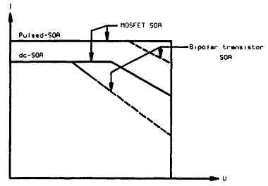
FIG. 31 SOA curves for power MOSFET
5.8 Practical Components
5.8.1 High Voltage and Low On Resistance Devices
Denser geometries, processing innovations, and packaging improvements are resulting in power MOSFETs that have ever-higher voltage ratings and current-handling capabilities, as well as volumetric power-handling efficiency. See Travis (1989), Goodenough (1995), and Goodenough (1994) for more information. Bipolar transistors have always been available with very high voltage ratings, and those ratings do not carry onerous price penalties. Achieving good high-voltage performance in power MOSFETS, however, has been problematic, for several reasons.
First, the rDS(on) of devices of equal silicon area increases exponentially with the voltage rating. To get the on-resistance down, manufacturers would usually pack more parallel cells onto a die. But this denser packing causes problems in high-voltage performance. Propagation delays across a chip as well as silicon defects, can lead to unequal voltage stresses and even to localized breakdown.
Manufacturers resort to a variety of techniques to produce high voltage ( > 1000V), low-rDS(on) power MOSFETS that offer reasonable yields. Advanced Power Technology (APT), for example, deviates from the trend toward smaller and smaller feature sizes in its quest for low on-resistance. Instead, the company uses large dies to get rDS(on) down. APT manufactures power MOSFETS using dies as large as 585 x 738 mil and reaching voltage ratings as high as 1000V. APT10026JN, a device from their product range has a current rating of 1000V with 690W power rating. On resistance of the device is 0.26f2.
When devices are aimed out to low power applications such as laptop and notebook computers, personal digital assistants (PDA), etc. extremely low RDS(on)values from practical devices are necessary.
Specific on-resistance of double-diffused MOSFETs (DMOSFETs), more commonly known as power MOSFETs, has continually shrunk over the past two decades. In other words, the RDS(on) per unit area has dropped. The reduced size with regard to low-voltage devices (those rated for a maximum drain-to-source voltage, VDS of under 100 V) was achieved by increasing the cell density.
Most power-MOSFET suppliers now offer low-voltage FETs from processes that pack 4,000,000 to 8,000,000 cells/in 2, in which each cell is an individual MOSFET. The drain, gate, and source terminals of all the cells are connected in parallel.
Manufacturers such as International Rectifier (IOR) have developed many generations of MOSFETs based on DMOS technology. For example, the HEXFET family from IOR has gone through five generations, gradually increasing the number of cells per in 2 with almost 10 fold decrease in the RDS(on) parameter as per FIG. 32. RDS(on) times the device die area in this figure is a long used figure of merit (FOM) for power semiconductors. This is called "specified on resistance." For details Kinzer (1995) is suggested.
Because generation 5 die are smaller than the previous generation, there is room within the same package to accommodate additional devices such as a Schottky diode. The FETKY family from IOR (Davis 1997) which uses this concept of integrating a MOSFET with a Schottky diode is aimed for power converter applications such as synchronous regulators, etc.
In designing their DMOSFETs, Siliconix borrowed a DRAM process technique called the trench gate. They then developed a low voltage DMOSFET process that provides 12,000,000 cells/in 2, and offers lower specific on-resistance m RDs(on)wthan present planar processes.
The first device from the process, the n-channel Si4410DY, comes in Siliconix's data book "Little Foot" 8-pin DIP. The Si4410DY sports a maximum on resistance of 13.5 m Q, enhanced with 10V of gate-to-source voltage (VGs). At a VGS of 4.5 V RDS(on) nearly doubles, reaching a maximum value of 20 m~. During the year 1997 Temic Semiconductors (formerly Siliconix) has further improved their devices to carry 32 million cells/in s using their "TrenchFET" technology. These devices come in two basic families namely (i) Low-on resistance devices and (ii) Low-threshold devices. Maximum on-resistance were reduced to 9mf~ and 13m~, compared to the case of Si 4410DY devices with corresponding values of 13.5mfl (for VGS of 10V) and 20mf~ (for VGS of 4.5V), for these low on resistance devices. In the case of low-threshold family these values were 10 mf~ and 14 mf~ for gate source threshold values of 4.5V and 2.5V respectively. For details Goodenough (1997) is suggested.
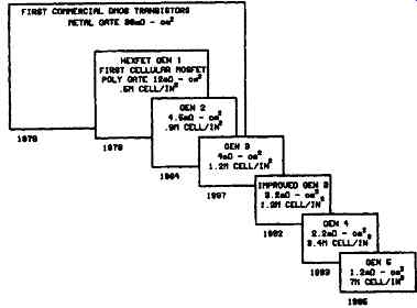
FIG. 32 The Power MOSFETs Generations (Courtesy: International Rectifier)
5.8.2 P-Channel MOSFETs
Historically, p-channel FETs were not considered as useful as their n-channel counterparts. The higher resistivity of p-type silicon, resulting from its lower carder mobility, put it at a disadvantage compared to n-type silicon.
Due to the approximately 2:1 superior mobility on n-type devices, n-channel power FETs dominate the available devices, because they need about half the area of silicon for a given current or voltage rating. However, as the technology matures, and with the demands of power-management applications, p-channel devices are starting to become available.
They make possible power CMOS designs and eliminate the need for special high-side drive circuits. When a typical n-channel FET is employed as a high-side switch running off a plus supply rail with its source driving the load, the gate must be pulled at least 10 V above the drain. A p-channel FET has no such requirement.
A high-side p-channel MOSFET and a low-side n-channel MOSFET tied with common drains make a superb high-current "CMOS equivalent" switch.
Because on-resistance rises rapidly with device voltage rating, it was only recently (1994/1995) high voltage p-channel Power MOSFETS were introduced commercially. One such device is IXTHIlP50 from IXYS Semiconductors with a voltage rating of 500V and current rating of 11A and an on-resistance of 900mΩ. Such high-current devices eliminate the need to parallel many lower-current FETs. These devices make possible complementary high-voltage push-pull circuits and simplified half-bridge and H bridge motor drives.
Recently introduced low voltage p MOSFETs from the TrenchFET family of Temic Semiconductors (Goodenough, 1997) have typical rDS(on) values between 14mΩ to 25mΩ.
5.8.3 More Advanced Power MOSFETS
With the advancement of processing capabilities, industry benefits with more advanced Power MOSFETS such as: (a) Current sensing MOSFETS (b) Logic-level MOSFETS

FIG. 33 Advanced Monolithic MOSFETS (a) Current sensing MOSFET (b) Application
of a logic-level MOSFET(c) Current limiting MOSFET (d) Voltage clamping, current
limiting MOSFET (c) Current limiting MOSFETS (d) Voltage clamping, current
limiting MOSFETS
The technique of current minoring for source current-sensing purposes involves connecting a small fraction of the cells in a power MOSFET to a separate sense terminal. The current in this terminal (see FIG. 33(a)) is a fixed fraction of the source current feeding the load. Current sense lead provides an accurate fraction of the drain current that can be used as a feedback signal for control and/or protection.
It's also valuable if you must squeeze the maximum switching speed from a MOSFET. For example, you can use the sense terminal to eliminate the effects of source-lead inductance in high-speed switching applications. Several manufacturers such as Harris, IXYS, Phillips, etc. manufacture these components.
Another subdivision of the rapidly diversifying power-MOSFET market is a class of devices called logic-level FETs. Before the advent of these units, drive circuitry had to supply gate-source turn-on levels of 10V or more. The logic-level MOSFETS accept drive signals from CMOS or TTL ICs that operate from a 5V supply. Suppliers of these types include International Rectifier, Harris, IXYS, Phillips-Amperex, and Motorola. Similarly other types described under (b) and (d) above are also available in monolithic form and some of there devices are categorized under "Intelligent Discretes."
6. Insulated Gate Bipolar Transistor (IGBT)
MOSFETs have become increasingly important in discrete power device applications due primarily to their high input impedance, rapid switching times, and low on-resistance. However, the on-resistance of such devices increases with increasing drain-source voltage capability, thereby limiting the practical value of power MOSFETs to application below a few hundred volts.
To make use of the advantages of power MOSFETs and BJTs together a newer device, Insulated Gate Bipolar Transistor (IGBT), has been introduced recently.
With the voltage-controlled gate and high-speed switching of a MOSFET and the low saturation voltage of a bipolar transistor, the IGBT is better than either device in many high power applications. It is a composite of a transistor with an N-Channel MOSFET connected to the base of the PNP transistor.
FIG. 34(a) shows the symbol and FIG. 34(b) shows the equivalent circuit. Typical IGBT characteristics are shown in FIG. 34(c). Physical operation of the IGBT is closer to that of a bipolar transistor than to that of a Power MOSFET. The IGBT consists of a PNP transistor driven by an N-channel MOSFET in a pseudo-Darlington Configuration.
The JFET supports most of the voltage and allows the MOSFET to be a low voltage type, and consequently have a low RDS(on) value. The absence of the integral reverse diode gives the user the flexibility of choosing an external fast recovery diode to match a specific requirement. This feature can be an advantage or a disadvantage, depending on the frequency of operation, cost of diodes, current requirement, etc.
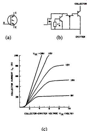
FIG. 34 IGBT (a) Symbol (b) Equivalent circuit (c) Typical output characteristics
In IGBTs on-resistance values have been reduced by a factor of about 10 compared with those of conventional n-channel power MOSFETs of comparable size and voltage rating.
IGBT power modules are rapidly gaining applications in systems such as inverters, UPS systems and automotive environments. The device ratings are reaching beyond 1800 volts and 600A. The frequency limits from early values of 5KHz are now reaching beyond 20KHz while intelligent IGBT modules that include diagnostic and control logic along with gate drive circuits are gradually entering the market.
Characteristics comparison of IGBTs, Power MOSFETs, Bipolars, and Darlingtons are indicated in Table 2. References listed between Russel (1992) through Clemente, Dubhashi, and Pelly (1990) provide more details on IGBTs and their applications.
====
TABLE 2 Characteristics Comparison of IGBTs, Power MOSFETs, Bipolars, and Darlingtons
Power MOSFETs-- IGBTs --Bipolars --Darlingtons
Type of Drive -- Voltage-- Voltage --Current-- Current
Drive Power Minimal Minimal Large Medium
Simple Simple Medium Drive Complexity Current Density for Given Voltage Drop Switching Losses High at Low Voltagem Low at High Voltages ,., Very Low Very High (small trade-off with switching speed)
..... Low to Medium (depending on trade-off with conduction losses)
High (large positive and negative currents are required)
Medium (severe trade-off with switching speed)
Medium to High (depending on trade-off with conduction losses)
Low High
====
7. MOS Controlled Thyristor (MCT)
MOS Controlled Thyristors are a new class of power semiconductor devices that combine thyristor current and voltage capability with MOS gated turn-on and turn-off. Various sub-classes of MCTs can be made: P-type or N-type, symmetric or asymmetric blocking, one or two-sided Off-FET gate control, and various turn-on alternatives including direct turn-on with light.
All of these sub-classes have one thing in common; turn-off is accomplished by turning on a highly interdigitated Off-FET to short out one or both of the thyristor's emitter-base junctions. The device, first announced a few years ago by General Electric's power semiconductor operation (now part of Harris Semiconductor, USA), was developed by Vic Temple. Harris is the only present (1997) supplier of MCTs, however ABB has introduced a new device called "Insulated Gate Commutated Thyristor" (IGCT) which is in the same family of devices.
FIG. 35 depicts the MCT equivalent circuit. Most of the characteristics of an MCT can be understood easily by reference to the equivalent circuit shown here.
MCT closely approximates a bipolar thyristor (the two transistor model is shown) with two opposite polarity MOSFET transistors connected between its anode and the proper layers to turn it on and off. Since MCT is a NPNP device rather than a PNPN device and output terminal or cathode must be negatively biased.
Driving the gate terminal negative with respect to the common terminal or anode turns the P channel FET on, firing the bipolar SCR. Driving the gate terminal positive with respect to the anode turns on the N channel FET on shunting the base drive to PNP bipolar transistor making up part of the SCR, causing the SCR to turn off. It is obvious from the equivalent circuit that when no gate to anode voltage is applied to the gate terminal of the device, the input terminals of the bipolar SCR are unterminated. Operation without gate bias is not recommended.
In the P-MCT a P-channel On-FET is turned on with a negative voltage which charges up the base of the lower transistor to latch on the MCT. The MCT turns on simultaneously over the entire device area giving the MCT excellent di/dt capability.
FIG. 36 compares different 600V power switching devices. FIG. 37 compares the characteristics of 1000 V P-MCT device with a N-IGBT device of same voltage rating. Note that the MCT typically has 10 to 15 times the current capability at the same voltage drop.
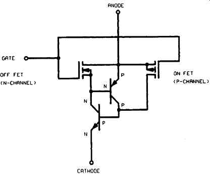
FIG. 35 MCT equivalent circuit
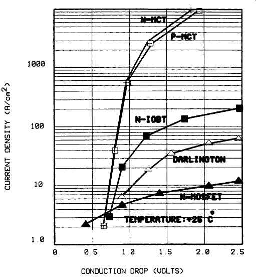
FIG. 36 Comparison of 600 V devices (Harris Semiconductor Sector)
The MCT will remain in the on-state until current is reversed (like a normal thyristor) or until the off-FET is activated by a positive gate voltage. Just as the IGBT looks like a MOSFET driving a BJT, the MCT looks like a MOSFET driving a thyristor (an SCR). SCRs and other thyristors turn on easily, but their turn-off requires stopping, or diverting virtually all of the current flowing through them for a short period of time. On the other hand, the MCT is turned off with voltage control on the high-impedance gate. The MCT offers a lower specific on-resistance at high voltage than any other gate-driven technology.
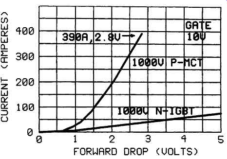
FIG. 37 Comparison of forward voltage drop of 1000V P-MCT and N-IGBT at
150°C (Harris
Semiconductor Sector)
That is, just as the IGBT operates at a higher current density than the DMOSFET, the MCT (like all thyristors) operates at even higher current densities. In the future, the ultimate power switch may well be the MOS-controlled thyristor (MCT). References 16 to 20 provide details for designers.