AMAZON multi-meters discounts AMAZON oscilloscope discounts
1. Introduction
During the elapsed half century from the invention of the transistor, the power electronics world has been able to enjoy the benefit of many different types of power semiconductor devices. These devices are able to handle voltages from few volts to several kilovolts, switching currents from few milliamperes to kiloamperes.
Within a decade from the invention of transistor, the thyristor was commercialized.
Around 1968 power transistors began replacing the thyristors in switchmode power systems. The power MOSFET, as a practical commercial device, has been available since 1976. When "smart power" devices appeared in the market, designers were able to make use of the Insulated Gate Bipolar Transistor (IGBT) from the early 90s. In 1992 MOS controlled thyristors were commercially introduced and around 1995, semiconductor materials such as GaAs and Silicon Carbide (SIC) have opened new vistas for better performance power diodes for high frequency switching systems.
Presently, the spectrum of what are referred to as "power devices" spans a very wide range of devices and technology. Discrete power semiconductors will continue to be the leading edge for power electronics in the 1990s. Improvements on the fabrication processes for basic components such as diodes, thyristors, and bipolar power transistors have paved way to high voltage, high current, and high speed devices. Some major players in the industry have invested in manufacturing capabilities to transfer the best and newest power semiconductor technologies from research areas to production.
Commercially available power semiconductor devices could be categorized in to several basic groups such as, diodes, thyristors, bipolar junction power transistors (BJT), power metal oxide silicon field effect transistors (Power MOSFET), insulated gate bipolar transistors (IGBT), MOS controlled thyristors (MCT), and gate turn off thyristors (GTO), etc. This section provides an overview of the characteristics, performance factors, and limitations of these device families.
2. Power Diodes and Thyristors
2.1 Power Diodes
The diode is the simplest semiconductor device, comprising a P-N junction.
In attempts to improve its static and dynamic properties, numerous diode types have evolved. In power applications diodes are used principally to rectify, that is, to convert alternating current to direct current. However, a diode is used also to allow current freewheeling. That is, if the supply to an inductive load is interrupted, a diode across the load provides a path for the inductive current and prevents high voltages L di/ dt damaging sensitive components of the circuit.
The basic parameters characterizing the diodes are its maximum forward average current IF(Ave) and the peak inverse voltage (PIV) 1. This parameter is sometimes termed as blocking voltage (Vrrm). There are two main categories of diodes, namely "general purpose P-N junction rectifiers" and "fast recovery P-N junction rectifiers." General purpose types are used in circuits operating at the line frequencies such as 50 or 60 Hz. Fast recovery (or fast turn-off) types are used in conjunction with other power electronics systems with fast switching circuits.
Classic examples of the second type are switchmode power supplies (SMPS) or Inverters, etc. FIG. 1(a) indicates the capabilities of a power device manufacturer catering for very high power systems and FIG. 1(b) indicates the capabilities of a manufacturer catering for a wide range of applications.
At high frequency situations such as Inverters and SMPS, etc., two other important phenomena dominate the selection of rectifiers. Those are the "forward recovery" and the "reverse recovery."
2.1.1 Forward Recovery
The turn-on transient can be explained with FIG. 2. When the load time constant L/R is long compared to the time for turn on tfr (forward recovery time) load current will hardly change during this period. For the time t< 0, the switch Sw is closed. Steady conditions prevail and the diode D is reverse biased at -V s. It is in the off-state, and i_D =0.
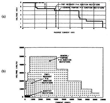
FIG. 1 Rectifier capabilities (a) Rectifier capabilities of a major supplier
of high power semiconductors (Reproduced by permission of GEC Plessey Semiconductors,
UK.) (b) Rectifier capabilities of a manufacturer catering for wide range
of applications (court. International Rectifier Inc.,
USA.)
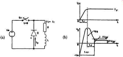
FIG. 2 Turn on characteristics (a) Circuit (b) Waveforms
At t=0, the switch Sw is opened. The diode becomes forward biased, provides a path for the load current in R and L, so that the diode current i_D rises to I F (I 0 after a short time t r (rise time) and the diode voltage drop falls to its steady value after a further time tf (fall time). This is shown in FIG. 2(b). The diode turn-on time is the time tfr, that comprises tr+ tf. It takes this time tfr for charge to change from one equilibrium state (off) to the other (on).
The total drop V D reaches a peak forward value VFR that may be from 5 to 20V, a value much greater than the steady value VDF generally between 0.6 to around 1.2V. The time t r for the voltage to reach VFR is usually about 0.11xs. At a time t > t r, the current i o becomes constant at I 1 (which will be the forward diode current IF). Further, conductivity modulation takes place due to the growth of excess cartiers in the semiconductor accompanied by a reduction of resistance. Consequently, the iDR D voltage drop reduces. In the equilibrium state, that may take a time of tf, with a uniform distribution of excess carders, the voltage drop v D reaches its minimum steady-state value VDF. During the turn-on interval tf, the current is not uniformly distributed so the current density can be high enough in some parts to cause hot spots and possible failure. Accordingly, the rate of rise of current diD/dt should be limited until the conduction spreads uniformly and the current density decreases. Associated with the high voltage VFR at turn-on, there is high current, so there is extra power dissipation that is not evident from the steady-state model. The turn-on time varies from a few ns to about l ms depending on the device type.
2.1.2 Reverse Recovery
Turn-off phenomenon can be explained using FIG. 3. In FIG. 3(a) except for the diode, the circuit elements of this simple chopper are considered to be ideal. Switching Sw at a regular frequency, the source of constant voltage, Vs maintains a constant current I_l in the RL load, because it is assumed that the load time constant L/ R is long compared with the period of the switching.
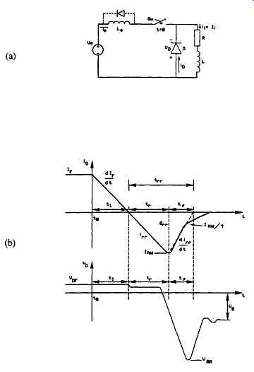
FIG. 3 Diode turn-off (a) Chopper circuit (b) Waveforms
While the switch Sw is closed, the load is being charged and the diode should be reverse biased. While the switch Sw is open, the diode D provides a freewheeling path for the load current I l. The inductance Ls is included for practical reasons and may be the lumped source inductance and snubber inductance, that should have a freewheeling diode to suppress high voltages when the switch is opened.
Let us consider that steady conditions prevail. At the time t = 0 the switch Sw is open, the load current is i_l = I_l, the diode current is i_D = I l = I F, and the voltage drop V o across the diode is small ( about 1V). The important concern is what happens after the switch is closed at t = 0. FIG. 3(b) depicts the Waveforms of the diode current i_D and voltage v D. At t = 0 there was the excess charge cartier distribution of conduction in the diode. This distribution cannot change instantaneously so at t = 0 ÷ the diode still looks like a virtual short circuit, with v D = 1V. Kirchhoff's current law provides us with the relation:
iD =ll - i s (eqn. 1)
and Kirchhoff's voltage law yields:
![]() (eqn. 2)
(eqn. 2)
Accordingly, the diode current changes at the rate,
diD/dt = Vs/Ls= Constant eqn.3)
This means that it takes a time t1 =Ls (I(l/Vs) seconds for the diode current to fall to zero.
At the time t = t I the current iD is zero, but up to this point the majority carriers have been crossing the junction to become minority carders, so the P-N junction cannot assume a blocking condition until these carriers have been removed. At zero current, the diode is still a short circuit to the source voltage. Equations (1) to ( 3) still apply and the current i_D rises above I_l at the same rate. The diode voltage V D changes little while the excess carders remain. The diode reverse current rises over a time t τ during which the excess charge carriers are swept out of the region.
At the end of the interval t τ the reverse current i_D can have risen to a substantial value IRR (peak reverse recovery current), but, by this time, sufficient carriers have been swept out and recombined that current cannot be supported. Therefore, over a fall-time interval tf the diode current i_D reduces to almost zero very rapidly while the remaining excess carders are swept out or recombined.
It is during the interval tf that the potential barrier begins to increase both to block the reverse bias voltage applied by the source voltage as i_D reduces, and to suppress the diffusion of majority carriers because the excess carder density at the junction is zero. The reverse voltage creates the electric field that allows the depletion layer to acquire space charge and widen.
That is, the electric field causes electrons in the n region to be forced away from the junction towards the cathode and causes holes to be forced away from the junction towards the anode. The blocking voltage v D can rise above the voltage V s di o transiently because of the additional voltage Ls ~ as i_D falls to zero over the time tf.
The sum of the intervals t τ + tf = trr is known as the reverse recovery time and it varies generally (between 10 ns to over 1 microsecond) for different diodes. This time is also known as the storage time because it is the time that is taken to sweep out the excess charge QRR from the silicon by the reverse current. QRR is a function of I D = I 1, did and the junction temperature. It has an effect on the reverse recovery dt current IRR and the reverse recovery time trr, so it is usually quoted in the data sheets. The fall time tf can be influenced by the design of the diode. It would seem reasonable to make it short to decrease the turn-off time, but the process is expensive. The bulk of the silicon can be doped with gold or platinum to reduce carder lifetimes and hence to reduce tf. The advantage is an increased frequency of switching.
There are two disadvantages associated with this gain in performance. One is an increased on-state voltage drop and the other is an increased voltage recovery di s overshoot VRR, that is caused by the increased Ls ~ as i_D falls more quickly.
Of the two effects, reverse recovery usually results in the greater power loss, and can also generate significant EMI. However these phenomena were considered to be no big deal at 50 or 60Hz. With the advent of semiconductor power switches, power conversion began to move into the multi-kilohertz range, and faster rectifiers were needed.
The relatively long minority carrier lifetime in silicon (tens of microseconds) causes a lot more charge to be stored than is necessary for effective conductivity modulation. In order to speed up reverse recovery, early "fast" rectifiers used various lifetime killing techniques to reduce the stored minority charge in the lightly doped region. The reverse recovery times of these rectifiers were dramatically reduced, down to about 200ns, although forward recovery and forward voltage were moderately increased as a side effect of the lifetime killing process. As power conversion frequencies increased to 20kHz and beyond, there eventually became a growing need for even faster rectifiers, which caused the "epitaxial" rectifier to be developed.
2.1.3 Fast and Ultra Fast Rectifiers
The foregoing discussion reveals the importance of the switching parameters such as (i) forward recovery time (tfr), (ii) forward recovery voltage (VFR), (iii) reverse recovery time (trr), (iv) reverse recovery charge (Qrr), and (v) reverse recovery current IRM, etc., during the transition from forward to reverse and vice versa.
With various process improvements fast and ultrafast rectifiers have been achieved within the voltage and current limitations shown in FIG. 1.
The figure shows that technology is available for devices up to 2000V ratings and over 1000 A current ratings which are mutually exclusive. In these diodes although cold trr values are good, at high junction temperature trr is three to four times higher, increasing switching losses and, in many cases, causing thermal runaway.
There exist several methods to control the switching characteristics of diodes and each leads to a different interdependency of forward voltage drop V F, blocking voltage VRR M and trr values. It is these interdependencies (or compromises) that differentiate the ultrafast diodes available on the market today. The important parameters for the turn-on and turn-off behavior of a diode are VFR, V F, tfr, IRM and trr and the values vary depending on the manufacturing processes.
Several manufacturers such as IXYS Semiconductors, International Rectifier, etc. manufacture a series of ultrafast diodes, termed Fast Recovery Epitaxial Diodes (FRED), which has gained wide acceptance during the 1990s. For an excellent description of these components see Burkel and Schneider (1994).
2.1.4 Schoffky Rectifiers
Schottky rectifiers occupy a small comer of the total spectrum of available rectifier voltage and current ratings illustrated in FIG. 1(b). They are, nonetheless, the rectifier of choice for low voltage switching power supply applications, with output voltages up to a few tens of volts, particularly at high switching frequency. For this reason, Schottkys account for a major segment of today's total rectifier usage. The Schottkys' unique electrical characteristics set them apart from conventional P-N junction rectifiers, in the following important respects:
• Lower forward voltage drop
• Lower blocking voltage
• Higher leakage current
• Virtual absence of reverse recovery charge
The two fundamental characteristics of the Schottky that make it a winner over the P-N junction rectifier in low voltage switching power supplies are its lower forward voltage drop, and virtual absence of minority carder reverse recovery.
The absence of minority carrier reverse recovery means virtual absence of switching losses within the Schottky itself. Perhaps more significantly, the problem of switching voltage transients and attendant oscillations is less severe for Schottkys than for P-N junction rectifiers. Snubbers are therefore smaller and less dissipative.
The lower forward voltage drop of the Schottky means lower rectification losses, better efficiency, and smaller heat sinks. Forward voltage drop is a function of the Schottky's reverse voltage rating. The maximum voltage rating of today's Schottky rectifiers is about 150V. At this voltage, the Schottky's forward voltage drop is lower than that of a fast recovery epitaxial P-N junction rectifier by 150 to 200mV. At lower voltage ratings, the lower forward voltage drop of the Schottky becomes progressively more pronounced, and more of an advantage. A 45V Schottky, for example, has a forward voltage drop of 0.4 to 0.6V, versus 0.85 to 1.0 V for a fast epitaxial P-N junction rectifier. A 15V Schottky has a mere 0.3 to 0.4V forward voltage drop.
A conventional fast recovery epitaxial P-N junction rectifier, with a forward voltage drop of 0.9V would dissipate about 18 percent of the output power of a 5V supply. A Schottky, by contrast, reduces rectification losses to the range of 8 to 12 percent. These are the simple reasons why Schottkys are virtually always preferred in low voltage high frequency switching power supplies. For any given current density, the Schottky's forward voltage drop increases as its reverse repetitive maximum voltage (VRR M) increases. The basic hallmarks of any process are its maximum rated junction temperature--the Tjmax Class and the "prime" rated voltage, the Vrr m Class. These two basic hallmarks are set by the process; they in turn determine the forward voltage drop and reverse leakage current characteristics.
FIG. 4 indicates this condition for Tjmax of 150°c.
FIG. 4 Relationships between Schottky VRRM Class and forward voltage drop, for 150°c Tjmax class devices (International Rectifier, USA)
2.1.4.1 Leakage Current and Junction Capacitance of Schottky Diodes
FIG. 5 shows the dependence of leakage current on the operating voltage and junction temperature within any given process. Reverse leakage current increases with applied reverse voltage, and with junction temperature. FIG. 6 shows typical relationship between operating temperature and leakage current, at rated VRR M, for the 150°C/45V and 175°C/45V Schottky processes.
An important circuit-characteristic of the Schottky is its junction capacitance.
This is a function of the area and thickness of the Schottky die, and of the applied voltage. The higher the VRR M class, the greater the die thickness and the lower the junction capacitance. This is illustrated in FIG. 7. Junction capacitance is essentially independent of the Schottky's Tjmax Class, and of operating temperature.
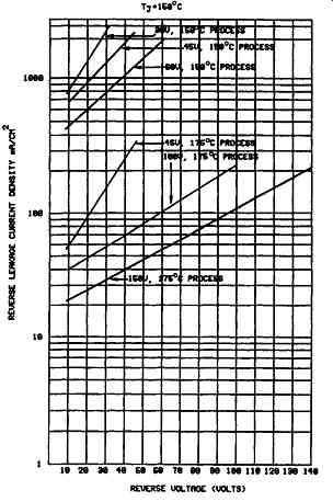
FIG. 5 Relationships between reverse leakage current density, and applied
reverse voltage (Reproduced by permission of International Rectifier, USA)
2.1.5 GaAs Power Diodes
Efficient power conversion circuitry requires rectifiers that exhibit low forward voltage drop, low reverse recovery current, and fast recovery time. Silicon has been the material of choice for fast, efficient rectification in switched power applications. However, technology is nearing the theoretical limit for optimizing reverse recovery in silicon devices.
To increase speed, materials with faster carrier mobility are needed. Gallium Arsenide (GaAs) has a carrier mobility which is five times that of silicon (Delaney, Salih, and Lee 1995). Since Schottky technology for silicon devices is difficult to produce at voltages above 200V, development has focused on GaAs devices with ratings of 180V and higher. The advantages realized by using GaAs rectifiers include fast switching and reduced reverse recovery related parameters. An additional benefit is the variation of parameters with temperature is much less than silicon rectifiers.
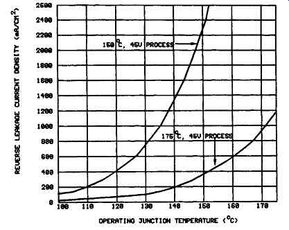
FIG. -6 Typical relationships between reverse leakage current density,
and operating junction temperature (Reproduced by permission of International
Rectifier, USA)
For example, Motorola's 180V and 250V GaAs rectifiers are being used in power converters that produce 24, 36, and 48V DC outputs. Converters producing 48V DC, specially popular in telecommunications and mainframe computer applications, could gain the advantage of GaAs parts compared to similar silicon based parts at switching frequencies around 1 MHz (Deuty 1996).
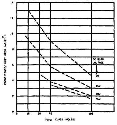
FIG. 7 Typical Schottky self-capacitance versus VRR M class, measured at
various bias voltages (Reproduced by permission of International Rectifier,
USA) The 180V devices offered by Motorola can increase power density in 48V
DC applications up to 90W/in 3 (21). These devices allow designers to switch
converters at 1MHz without generating large amounts of EMI.
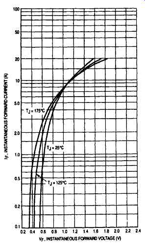
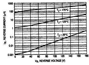
FIG. 8 Typical characteristics of GaAs power diodes with 20A, 180V ratings (a)
Forward voltage (b) Reverse current (Copyright of Motorola, used by permission)
FIG. 8(a) [top] and [above] 8(b) indicate typical forward voltage and typical reverse current for 20A, 180V, GaAs parts from Motorola.
For further details, the reader is directed to the following references: (Ashkanazi, Lorch and Nathan 1995), (Delaney, Salih, and Lee 1995), and (Deuty 1996).
2.2 Thyristors
The thyristor is a four-layer, three-terminal device as depicted in FIG. 9.
The complex interactions between three internal P-N junctions are then responsible for the device characteristics. However, the operation of the thyristor and the effect of the gate in controlling turn-on can be illustrated and followed by reference to the two transistor model of FIG. 10. Here, the Pl-nvP2 layers are seen to make up a p-n-p transistor and the n2-P2-n I layers create a n-p-n transistor with the collector of each transistor connected to the base of the other.
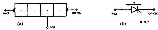
FIG. 9 The thyristor (a) Construction (b) Circuit symbol
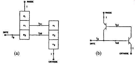
FIG. 10 The two transistor model of a thyristor (a) Structure (b) The p-n-p
and n-p-n transistor combination.
With a reverse voltage, cathode positive with respect to the anode, applied to the thyristor the p1-n1 and p2-n2 junctions are reverse biased and the resulting characteristic is similar to that of the diode with a small reverse leakage current flowing up to the point of reverse breakdown as shown by FIG. 11(a). With a forward voltage, applied and no gate current supported the thyristor is in the forward blocking mode. The emitters of the two transistors are now forward biased and no conduction occurs. As the applied voltage is increased, the leakage current through the transistors increases to the point at which the positive feedback resulting from the base/collector connections drives both transistors into saturation, turning them, and hence the thyristor, on. The thyristor is now conducting and the forward voltage drop across it falls to a value of the order of 1 to 2 V. This condition is also shown in the thyristor static characteristic of FIG. 11(a). If a current is injected into the gate at a voltage below the breakover voltage, this will cause the n-p-n transistor to turn on. The positive feedback loop will then initiate the turn on of the p-n-p transistor. Once both transistors are on, the gate current can be removed because the action of the positive feedback loop will be to hold both transistors, and hence the thyristor, in the on state.
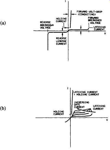
FIG. 11 Thyristor characteristics (a) Thyistor characteristics with zero
gate current (b) Switching characteristics
The effect of the gate current is therefore to reduce the effective voltage at which forward breakover occurs, as illustrated by the FIG. 11(b). After the thyristor has been turned on it will continue to conduct as long as the forward current remains above the holding current level, irrespective of gate current or circuit conditions.
2.2.1 Ratings and Different Types of Devices
The operation of all power semiconductors is limited by a series of ratings which define the operating boundaries of the device. These ratings include limits on the peak, average and RMS currents, the peak forward and reverse voltages for the devices, maximum rates of change of device current and voltage, device junction temperature and, in the case of the thyristor, the gate current limits.
The current ratings of a power semiconductor are related to the energy dissipation in the device and hence the device junction temperature. The maximum value of on-state current (Iav(max)) is the maximum continuous current the device can sustain under defined conditions of voltage and current Waveform without exceeding the permitted temperature rise in the device. The rms current rating (IRM s) is similarly related to the permitted temperature rise when operating into a regular duty cycle load.
In the case of transient loads, as the internal losses and hence the temperature rise in a power semiconductor are related to the square of the device forward current, the relationship between the current and the permitted temperature rise can be defined in terms of an i2dt rating for the device. On turn-on, current is initially concentrated into a very small area of the device cross-section and the device is therefore subject to a di/dt rating which sets a limit to the permitted rate of rise of forward current.
The voltage ratings of a power semiconductor device are primarily related to the maximum forward and reverse voltages that the device can sustain. Typically, values will be given for the maximum continuous reverse voltage (VRC(max)), the maximum repetitive reverse voltage (VRR(max)) and the maximum transient reverse voltage (VRT(max)). Similar values exist for the forward voltage ratings.
The presence of a fast transient of forward voltage can cause a thyristor to turn on and a dv/dt rating is therefore specified for the device. The magnitude of the imposed dv/dt can be controlled by the use of a snubber circuit connected in parallel with the thyristor. Data sheets for thyristors always quote a figure for the maximum surge current ITS M that the device can survive.
This figure assumes a half sine pulse with a width of either 8.3 or 10 msec, which are the conditions applicable for 60 or 50Hz mains respectively. This limit is not absolute; narrow pulses with much higher peaks can be handled without damage, but little information is available to enable the designer to determine a current rating for short pulses. Hammerton (1989) indicates guidelines in this area.
Ever since its introduction, circuit design engineers have been subjecting the thyristor to increasing levels of operating stress and demanding that these devices perform satisfactorily there. The different stress demands that the thyristor must be able to meet are:
(a) Higher blocking voltages (b) More current carrying capability (c) Higher di/dt's (d) Higher dv/dt's (e) Shorter turn-off times (f) Lower gate drive (g) Higher operating frequencies.
There are many different thyristors available today which can meet one or more of these requirements, but as always, an improvement in one characteristic is usually only gained at the expense of another. As a result, different thyristors have been optimized for different applications. Modem thyristors can be classified into several general types, namely:
(a) Phase Control Thyristors (b) Inverter Thyristors
(c) Asymmetrical Thyristors (d) Reverse Conducting Thyristors (RCT) (e) Light-Triggered Thyristors.
The voltage and current capabilities of phase control thyristors and inverter thyristors from a power device manufacturer are summarized in FIG. 12.
2.2.1.1 Phase Control Thyristors
"Phase Control" or "Converter" thyristors generally operate at line frequency.
They are turned off by natural commutation and do not have special fast-switching characteristics.
Current ratings of phase-control thyristors cover the range from a few amperes to about 3500A, and the voltage ratings from 50 to over 6500V. To simplify the gate-drive requirement and increase sensitivity, the use of amplifying gate, which was originally developed for fast switching "inverter" thyristors, is widely adopted in phase control SCR.
2.2.1.2 Inverter Thyristors
The most common feature of an inverter thyristor which distinguishes it from a standard phase control type is that it has fast turnoff time, generally in the range of 5 to 50 laS, depending upon voltage rating. Maximum average current ratings of over 2000 and 1300 A have been achieved with 2000 and 3000 V rated inverter thyristors, respectively.
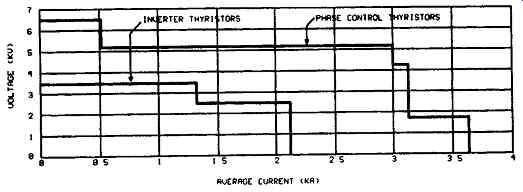
FIG. 12 Thyristor rating capabilities (GEC Plessey Semiconductors, UK)
Inverter thyristors are generally used in circuits that operate from DC supplies, where current in the thyristor is turned off either through the use of auxiliary comutating circuitry, by circuit resonance, or by "load" commutation. Whatever the circuit turn-off mechanism, fast turn-off is important because it minimizes sizes and weight of comutating and/or reactive circuit components.
2.2.1.3 Asymmetrical Thyristors
One of the main salient characteristics of asymmetrical thyristors (ASCR) is that they do not block significant reverse voltage. They are typically designed to have a reverse blocking capability in the range of 400 to 2000V. The ASCR finds applications in many voltage-fed inverter circuits that require anti-parallel feedback rectifiers that keep the reverse voltage to less than 20V. The fact that ASCR needs only to block voltage in the forward direction provides an extra degree of freedom in optimizing turn-off time, turn-on time, and forward voltage drop.
2.2.1.4 Reverse Conducting Thyristors
The reverse conducting thyristor (RCT) represents the monolithic integration of an asymmetrical thyristor with an anti-parallel rectifier. Beyond obvious advantages of the parts count reduction, the RCT eliminates the inductively induced voltage within the thyristor-diode loop (virtually unavoidable to some extent with separate discrete components). Also, it essentially limits the reverse voltage seen by the thyristor to only the conduction voltage of the diode.
2.2.1.5 Light-Triggered Thyristors
Many developments have taken place in the area of light-triggered thyristors.
Direct irradiation of silicon with light created electron-hole pairs which, under the influence of an electric field, produce a current that triggers the thyristors.
The turn-on of a thyristor by optical means is an especially attractive approach for devices that are to be used in extremely high-voltage circuits. A typical application area is in switches for DC transmission lines operating in the hundreds of kilovolts range, which use series connections of many devices, each of which must be triggered on command. Optical firing in this application is ideal for providing the electrical isolation between trigger circuits and the thyristor which floats at a potential as high as hundreds of kilovolts above ground.
The main requirement for an optically-triggered thyristor is high sensitivity while maintaining high dv/dt and di/dt capabilities. Because of the small and limited quantity of photo energy available for triggering the thyristor from practical light sources, very high gate sensitivity of the order of 100 times that of the electrically triggered device is needed.
=====
Above: TABLE 1 Thyristor Types and Popular Names JEDEC Titles
=====
2.2.1.6 JEDEC Titles and Popular Names
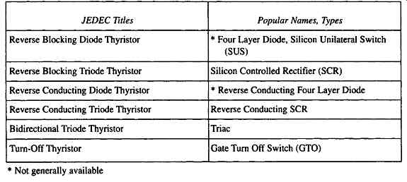
Table 1 compares the Joint Electronic Device Engineering Council (JEDEC) titles for commercially available thyristors types with popular names.
JEDEC is an industry standardization activity co-sponsored by the Electronic Industries Association (EIA) and the National Manufacturers Association (NEMA). Silicon controlled rectifiers (SCR) are the most widely used as power control elements. Triacs are quite popular in lower current (<40A) AC power applications.
3. Gate Turn-Off Thyristors
A gate turn-off thyristor (GTO) is a thyristor-like latching device that can be turned off by application of a negative pulse of current to its gate. This gate turn-off capability is advantageous because it provides increased flexibility in circuit application. It now becomes possible to control power in DC circuits without the use of elaborate commutation circuitry.
Prime design objectives for GTO devices are to achieve fast turn-off time and high current turn-off capability and to enhance the safe operating area during turnoff. Significant progress has been made in both areas during the last few years, largely due to a better understanding of the turn-off mechanisms. The GTO's turnoff occurs by removal of excess holes in the cathode-base region by reversing the current through the gate terminal.
The GTO is gaining popularity in switching circuits, especially in equipment which operates directly from European mains. The GTO offers the following advantages over a bipolar transistor: high blocking voltage capabilities, in excess of 1500V, and also high over-current capabilities. It also exhibits low gate currents, fast and efficient turn-off, as well as outstanding static and dynamic dv/dt capabilities.
FIG. 13(a) depicts the symbol of GTO and FIG. 13(b) shows its two transistor equivalent circuit. FIG. 13(c) shows a basic drive circuit. The GTO is turned on by a positive gate current, and it is turned off by applying a negative gate cathode voltage.
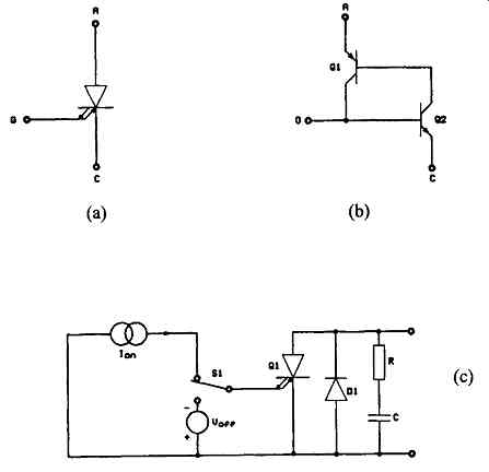
FIG. 13 GTO symbol, equivalent circuit & basic drive circuit (a) Symbol
of GTO (b) Two transistor equivalent of GTO (c) Basic drive circuit
A practical implementation of a GTO gate drive circuit is shown in FIG. 14. In this circuit when transistor Q2 is off, emitter follower transistor Q1 acts as a current source pumping current into the gate of the GTO through a 12-V Zener Z1 and polarized capacitor C1l. When the control voltage at the base of Q2 goes positive, transistor Q2 turns on, while transistor Q1 turns off since its base now is one diode drop more negative than its emitter. At this stage the positive side of capacitor C l is essentially grounded, and C1 will act as a voltage source of approximately 10V, turning the GTO off. Isolated gate drive circuits may also be easily implemented to drive the GTO.
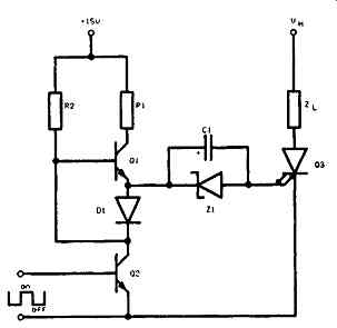
FIG. 14 Practical realization of a GTO gate drive circuit.
With improved cathode emitter geometries and better optimized vertical structures, today's GTOs have made significant progress in turn-off performance (the prime weakness of earlier day GTOs). FIG. 15 shows the available GTO ratings and, as can be seen, they cover quite a wide spectrum. However, the main applications lie in the higher voltage end (> 1200 V) where bipolar transistors and power MOSFETs are unable to compete effectively. In the present day market there are GTOs with current ratings over 3000A and voltage ratings over 4500V. For further details on GTOs see Coulbeck, Findlay, and Millington (1994) and Bassett and Smith (1989).