AMAZON multi-meters discounts AMAZON oscilloscope discounts
(cont. from part 1)
5. Resonant Converters
5.1 Introduction to Resonant Converters
The converters discussed so far, processed power in pulsed form, and are called Pulse Width Modulated (PWM) converters. The term resonance refers to a continuous sinusoidal signal. Resonant converters are those which process power in a sinusoidal form.
Resonant techniques have long been used with thyristor converters, in high-power SCR motor drives and in UPSs. However, due to its circuit complexity, it had not found application in low-power DC to DC converters until recently. However, due to certain advantages inherent in resonant techniques, and also due to the development of surface mount technology, resonant forms of DC to DC converters have gained rapid acceptance in this field of application.
The thrust towards resonant mode power supplies has been fueled by the industry's demand for miniaturization, together with increasing power densities and overall efficiency, and low EMI. With available devices and circuit technologies, PWM converters have been designed to operate with switching frequencies the range 50-200 kHz. With the advent of power MOSFETs enabled the switching frequencies to be increased to several MHz.
However, increasing the switching frequency, though allowing for miniaturization, leads to increasing switching stresses and losses. This leads to reduction in efficiency. The detrimental effects of the parasitic elements also become more pronounced as the switching frequency is increased. With quasi-resonant techniques, higher frequency as well as higher efficiency compared to PWM techniques are achieved.
Resonant circuits in power supplies operate in two modes that define the flow of current in the resonant circuit: continuous and discontinuous. In the continuous mode, the circuit operates either above or below resonance. The controller shifts the frequency either towards or away from resonance, using the slope of the resonant circuit's impedance curve to vary the output voltage. This is a truly resonant technique, but is not commonly used in power supplies due to its high peak currents and voltages.
In the discontinuous mode, the control circuit generates pulses having a fixed on-time, but at a varying frequency determined by the load requirements. This mode of operation does not generate continuous current flow in the tuned circuit. This is the common mode of operation in a majority of resonant converters, and is called the quasi-resonant mode of operation.
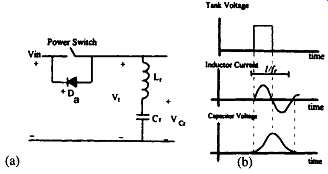
Above: Fig. 20 The resonant principle (a) The basic circuit (b) Associated
waveforms
5.2 The Quasi-Resonant Principle
The quasi-resonant principle is used in power converters by incorporating a resonant LC circuit with the power switch. The power switch is turned on and off in the same manner as in PWM converters, but the tank circuit forces the current through the switch into a sinusoidal form. The actual conduction period of the switch is governed by the resonant frequency f_r of the tank circuit. This basic principle is illustrated in Fig. 20. The tank circuit exhibits a relatively fixed ringing period to which the conduction period of the power switch is slaved. The ON period of the power switch is fixed to the resonance period of the tank elements. The quasi-resonant supply is controlled by changing the number of ON times of the power switch per second.
All resonant control circuits keep the pulse width constant and vary the frequency, whereas all PWM control circuits keep the frequency constant and vary the pulse width.
The main advantages of the quasi-resonance techniques arise from the sinusoidal waveshapes of the switching currents and voltages. The switching losses are reduced, leading to higher efficiency and EMI is greatly reduced.
5.3 PWM vs. Quasi-Resonant Techniques
The operation of a quasi-resonant switching power supply is analogous to a PWM supply of the same topology. The difference lies in the fact that the switching waveform in quasi-resonant supplies has been pre-shaped into a sinusoidal form.
Fig. 21 compares the switching waveforms of PWM and resonant converters. With PWM converters, there is simultaneous conduction of current and voltage during part of the switching period. In resonant conversion, switching can be achieved either at the zero current point or the zero voltage point of the sinusoidal switching waveform, thus minimizing the switching losses. However, increasing the switching frequency though allowing for miniaturization, is accompanied by increasing switching stresses, and detrimental effects due to parasitic elements.
The advantages and disadvantages of PWM and Quasi-Resonant conversion techniques are summarized in Table 2.
===
TABLE 2 Advantages and Disadvantages of Quasi Resonant Converters (QRCs) compared to PWM converters
Advantages:
• Lower switching losses, hence higher efficiency
• Lower EMI
• Higher maximum operating frequencies.
• Hence smaller size of components
Disadvantages:
• More complex circuit. Requires a longer design time and a higher level of expertise from the designer.
• Parasitic characteristics of components must be taken into account.
As current waveforms in quasi-resonant converters are sinusoidal, peak values are higher than those found in PWM converters.
• Increased device stress.
===
The major applications in which quasi-resonant technology finds acceptance today are those that require very low EMI levels, such as in aircraft, satellite, and audio/video equipment.
5.4 The Resonant Switch
The resonant switch consists of a semiconductor switch and resonant LC elements. Because resonant circuits generate sinusoidal waves, designers can operate the power switches either at zero current or at zero voltage points in the resonant waveform. Based on this, there are two types of resonant switches: zero current switches (ZCS) and zero voltage switches (ZVS). The two types of switches are the duals of each other. A description of the operations of these switches is also found in (Brown 1990).
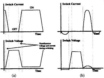
Above: Fig. 21 Comparison of switching waveforms in PWM and resonant
converters (a) PWM switching waveforms (b) Resonant switching waveforms
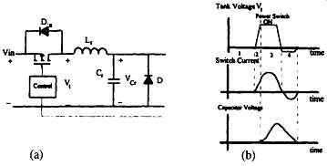
Above: Fig. 22 The zero-current quasi-resonant switch (a) The basic circuit
(b) Associated waveforms
5.4.1 Zero Current Quasi-Resonant Switches (ZC-QRCs)
A zero current quasi-resonant switch is shown in Fig. 22. The switch type shown is called a full wave switch where the antiparallel diode D a allows current to flow in either direction through the resonant circuit. Switches without such a diode allow only unidirectional current flow, and are called half wave switches. The operation of the switch can be broken down into four periods as shown in Fig. 22.
• Period 1" The power switch is off, and the diode D is conducting the load current.
• Period 2: The power switch turns on. The voltage across the switch makes a step change. The resonant capacitor appears to be short circuited at this time because of the conducting diode. Therefore, the power switch sees only the inductor on turning on. Therefore, the switch current cannot change instantaneously, and hence increases linearly from zero. This continues until all the load current is taken up by the current through the switch and the resonant inductor, displacing the current through the diode.
• Period 3: As the diode current is displaced, it turns off in a zero-current fashion, and the resonant capacitor is released into the circuit. Now, the current waveform assumes a sinusoidal shape as the circuit resonates. During this period, the capacitor voltage lags the current waveform by 90 °. The switch current proceeds over its crest, and passes through zero. The resonant inductor's current then starts to flow in the opposite direction through the antiparallel diode D_a.
• Period 4: When the inductor current passes through zero, the resonant capacitor begins to dump its charge into the load, thus reducing its voltage in a linear ramp. The diode begins to conduct. When the capacitor voltage reaches zero, the diode takes up the entire current, and the circuit awaits the next conduction period of the power switch.
As the power switch and diode operate at zero current on both edges, switching losses in the power semiconductors are greatly reduced. The ON period of the power switch is the resonant period of the tank circuit. The number of ON times per second is varied by the control circuits. This method of control is called the fixed on-time, variable off-time method.
For heavier loads, the number of resonant ON periods is higher. Therefore, to increase the output power, the controller increases the frequency. Converters using this type of switch are called parallel resonant converters because the load is placed in parallel with the resonant capacitor.
5.4.2 Zero Voltage Quasi-Resonant Switches (ZV-QRCs)
A zero voltage quasi-resonant switch is shown in Fig. 23. In this type, the power switch's OFF time is the resonant period. The operation of the switch can be broken down into four periods as shown.
• Period 1" The power switch is on. The switch current is determined by the converter stage configuration. The resonant inductor is saturated and is effectively short circuited. The input voltage appears across the resonant capacitor, and the diode D is off.
• Period 2: The resonant period is initiated by the power switch turning off.
As the voltage across the capacitor cannot change instantaneously, the power switch voltage remains constant while the current reduces to zero.
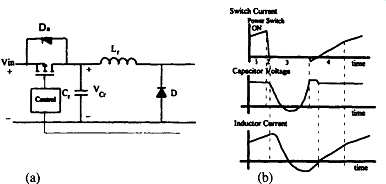
Above: Fig. 23 The zero-voltage quasi-resonant switch (a) The
basic-circuit (b) Associated waveforms
• Period 3: The capacitor voltage starts falling together with the inductor current. The diode starts to conduct, taking over the load current being from the resonant inductor which gradually falls out of saturation. The tank circuit begins to resonate. The capacitor voltage tings back above the input voltage, at which point the current is conducted by the antiparallel diode.
• Period 4: The power switch turns on. The diode D is also on at this time, and the capacitor is shunted out of the circuit. Therefore the switch current increases linearly through the resonant inductor. When this current exceeds the load current being conducted through the diode, the diode turns off. Then the resonant inductor can enter saturation and await the next cycle.
The number of OFF times per second is varied by the control circuits. This method of control is called the fixed off-time, variable on-time method. The "sense" of control is opposite to that in the ZCS. For heavier loads, the number of resonant OFF periods is decreased. Converters using this type of switch are called series resonant converters because the load is placed in series with the resonant inductor.
5.5 Quasi-Resonant Switching Converters
Comparable converter topologies as with the PWM technique are available with ZCS and ZVS quasi-resonant switching techniques. Circuits for each of these topologies are found in (Brown 1990), (Brown 1994), (Cuk and Middlebrook 1994), and (Steigerwald 1984). The available topologies for each type of switch are illustrated in Fig. 24 A quasi-resonant version of the Cuk converter is described in (Cuk and Maksimovic 1988).

Above: Fig. 24 Quasi-resonant converter topologies
ZCS-QR supplies present a high current stress upon the power switches and ZVS-QR supplies a high voltage stress. This causes some topologies to be better suited for certain ranges of input voltages and output powers. ZCS-QR supplies are good at high input voltages, but poor at high output powers. Conversely, ZVS-QR supplies are good at high output powers but poor at high input voltages.
For off-line applications and for switching frequencies up to 1 MHz, the ZCS technique is effective as it eliminates the switching stresses and the turn-off stresses.
However, the capacitive turn-on loss becomes high as the frequency is increased.
The ZVS technique minimizes the turn-on loss. However, the ZVS-QR switch suffers from two major limitations. One is due to the extensive voltage stress in single-ended configurations with wide load variations. Typically this stress is proportional to the load range, making them impractical for applications with a wide load range and/or high input current (Steigerwald 1984). The other limitation is related to the junction capacitance of the diode, which may cause undesirable oscillation with the resonant inductor.
Zero Voltage Switching
QR converters appear to be the more popular of the two quasi-resonant techniques. One reason for this is that the typical variation in frequency over its input and load variation is 4:1 for ZVS as opposed to 10:1 for ZCS. Secondly, they have a better heavy load performance, and their parasitic elements are more easily controlled. Most ZCR applications handle no more than 300 W of output power, whereas ZVS applications handle powers in excess of many kilowatts.
5.6 Control Techniques and ICs for Resonant Converters
Control methods for resonant converters are variable frequency ones. Either the on-time is fixed and the off time is variable or vice-versa. The basic functioning of a resonant mode control circuit is shown in Fig. 25. The fundamental blocks are a wide-band error amplifier, a voltage controlled oscillator (VCO) and a temperature-stable one-shot timer.
The output voltage is compared with the reference, and the error voltage is used to drive the VCO. The VCO output triggers the one-shot whose pulse duration is fixed as required by the converter. These control techniques are based on the voltage-mode of control, and hence suffer from poor input transient response characteristics.
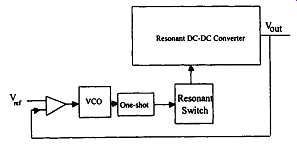
Above: Fig. 25 Resonant mode control
Some representative control ICs currently available are MC34066, LD405, UC1860, and UC3860. One of the first resonant mode controller ICs to appear on the market was the LD 405 by Gennum Corp. Subsequently, the CS3805 by Cherry Semiconductors and an improved GP605 by Gennum Corp. were released.
The LD405 and the CS3805 have drive current capabilities of 200 mA and operating frequencies in the range 10kHz to 1 MHz. They have single-ended and complementary outputs for driving power MOSFETs. The dissipation rate is specified at 500 mW at 50 ° C. The operating range of the GP605 is between 1 kHz and 1.2 MHz.
Unitrode Integrated Circuits introduced its UC3860 family of resonant mode controller chips in 1988. These were able to supply 800 mA, about 4 times the drive current and operate at higher frequencies (up to 2 MHz) than the previously available ICs. Their power dissipation rate is specified at 1.25W at 50 ° C. A newer series of resonant mode control chips by Unitrode Integrated Circuits and their applications are described in (Wofford 1990). These are the UC3860, UC1861 (dual ZVS), UC1864 (single ZVS), and UC1865 (dual ZCS). The functional block diagram of the UC1860 from Unitrode Integrated Circuits is shown in Fig. 26 (Unitrode Integrated Circuits 1995-1996). The nominal operating frequency for this IC is 1.5 MHz, and implements resonant-mode fixed-on-time control, as well as a number of other power supply control schemes with its various dedicated and programmable features. This IC contains dual high-current totem-pole output drivers which can be programmed to operate alternately or in unison (Unitrode Integrated Circuits 1995-1996). Although varying in detail and complexity all of these resonant mode control chips provide the same basic functions. All contain a VCO that varies the operating frequency, a monostable circuit that establishes the pulse on-time, and a steering circuit that determines the output drive mode (controlled on- or off-times, single-ended or complementary). The chips also provide many of the same basic protection features such as soft start, undervoltage lockout and overload protection--although in different ways and with varying degrees of sophistication.
Some of these control ICs are also described in (Brown 1990), (Brown 1994), and (Linear Technology Corp. 1994)-(Unitrode Integrated Circuits 1995-1996).
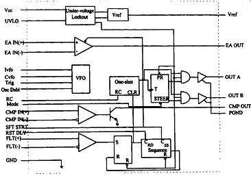
Above: Fig. 26 Functional block diagram of the UC 1860 Resonant Mode
Controller IC (Unitrode Integrated Circuits)
6 Special DC to DC Converter Designs
6.1 Sub-5V Applications
As IC process lithography becomes finer and the need to reduce overall power dissipation becomes more important, ICs demand lower and better regulated power supply rails. Power supply rails for modem microprocessors and logic ICs have dropped below 5V to a 3.3V pseudo standard, and are fast heading towards sub-2V and sub-IV levels. These low-voltage supply requirements also differ in voltage level from system to system, and from version to version of the same IC. Using Intel's Pentium as an example, some versions just require 3.3V while some require two supplies at 3.3 V and 3V. Yet other versions require supplies such as 3.383V and 3.525V, being the optimum voltages for maximum speed in the respective versions. Furthermore, the Pentium Pro comes with a 4-bit operating voltage code, which selects one of 16 discrete voltages between 2 to 3.5V (Travis 1996)-(Goodenough 1996). Lower voltage levels however, don’t translate to low power. These multi-million-transistor ICs use CMOS technology, which at today's high operating frequencies consume substantial amounts of current, though virtually no DC current. Power levels required are therefore rising.
Top-of-the line CPU power is approaching 100W, and desktop CPU power 30W. Systems such as high-performance multi-processor servers are approaching 400--600W. The combination of increasing power requirements and reducing voltage rails, requires the power source to provide and distribute very high currents within a system. For example, a 300W system running off a 3V supply must provide and distribute 100A of current.
Furthermore, clock rates heading towards 400-600 MHz imply high current transients as devices come out of the sleep mode within a clock cycle of a few nS. In addition to microprocessors, there are high-speed data buses such as the 60MHz GTL (Gunning Transceiver Logic) bus, that are being recommended for interconnection of processors and peripherals on the mother board. It requires an active 1.2V or 1.5V terminator at each end, each potentially capable of handling up to 7A. Other data buses with similar requirements include Futurebus (2.1V) and Rambus (2.7V) (Goodenough 1995). Therefore, the challenges facing the power supply designer in the sub 5-V range can be summarized as follows:
• Multiple voltage rails
• High efficiency while generating high currents (low power loss)
• Tight tolerances
• High accuracy
• High current transients
The basic design requirements in the face of these challenges are low power loss and higher gain and bandwidth in the control loop to handle tighter voltage regulation and transients.
6.2 Converters for Battery Operated Equipment and Battery Chargers
The proliferation of portable computers and hand-held communication devices has opened up another branch in DC/DC converter evolution. Users of these portable devices demand features such as compactness and lightness and low power consumption for extended periods of operation. Corresponding trends in DC/DC converters emphasize excellent conversion efficiency and compactness.
Additional constraints placed on the DC/DC converter include minimum noise intrusion into communications and audio circuits in the device. The increase in the integration of high-speed modems and CD ROM drives into portable computers has made power supply switching noise an important consideration.
A key requirement for designers of battery-powered products is that they minimize the number of cells used in the product. Products should ideally run off a few high-capacity cells to minimize size and cost. Tiny devices such as pagers run off one, or at most two, cells. So do telephones and PDAs. Converters operating off input sources as low as that of a single-cell alkaline battery (IV) are needed.
Therefore, the voltage required is in most instances, greater than the voltage available from the cells. Furthermore, for extended battery life, the converter should be able to operate from waning batteries.
Some systems need to operate with input voltages that approach the output voltage. This low dropout condition requires the DC/DC converter duty cycle to approach 100 percent. Furthermore, a waning battery may swing the input voltage from a value above the output to one below.
High efficiency is also a prime consideration in battery operated equipment.
It not only increases the operating time on a battery charge, but also reduces the heat which must be dissipated in or removed from the IC and the device. Low quiescent current is another requirement for extended battery charge.
Therefore, the challenges facing the power supply designer for battery powered applications can be summarized as follows:
- • Low drop-out voltage
- • Small size
- • Extended use of battery charge
- • Low EMI
6.3 Practical Design Approaches
This section describes some of the approaches taken in DC/DC converter and controller design to address the special requirements of sub-5V and battery powered applications. Illustrative examples of some successful solutions are presented.
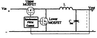
Above: Fig. 27 A synchronous buck converter
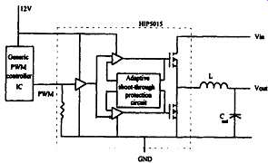
Above: Fig. 28 A PWM synchronous DC/DC converter using a SynchroFET (Copyright
by Harris Corporation, reprinted by permission of Harris Semiconductor
Sector)
6.3.1 Synchronous Rectification
In a conventional DC/DC converter such as the buck converter shown in Fig. 5, typically an n-channel MOSFET with a low RDS(on) is selected for the switch. However, the diode's forward voltage becomes a limiting factor in improving the converter's efficiency as the output voltage drops.
This has lead to the design of synchronous converters, which replace the diode which is normally a Schottky, with another N-channel MOSFET. This is usually called the lower MOSFET, and the switch is called the upper MOSFET. The lower MOSFET conducts current during the off time of the upper MOSFET. Fig. 27 shows a simplified diagram of a synchronous buck converter. Synchronous rectifiers are described further in Section 4 and (Sherman and Waiters 1996). In conventional synchronous converters, a single IC is used for PWM control and the synchronous drive of two external MOSFETs. Newer process technologies take another approach, where a SynchroFET integrates the two MOSFETS, their drive circuits and the synchronous control logic.
This IC can be used with a conventional PWM control IC to design a converter with superior features to those with discrete MOSFETs (Sherman and Waiters 1996). Also, this approach allows the SynchroFET to be paired with many different PWM controllers to achieve various performance trade-offs.
HIP5015 and HIP5016 are a widely used pair of SynchroFETs from Harris Semiconductor. A PWM 5V to 3.3V DC/DC converter using a genetic PWM controller and the HIP5015 SynchroFET is shown in Fig. 28. This is typically used to derive 3.3 V from a 5V input. The implementation of a two-output converter using these SynchroFET ICs is described in (Goodenough 1996). The HIPS015/5016 is designed to run at over 1 MHz. The efficiency of a 5 to 3.3V converter running at 400kHz using this IC is reported to be 85 percent for load currents between 0.5 and 4.5A and over 90% for load currents between 0.8 and 2.8a.
6.3.2 Increased Gain and Bandwidth Control Loop
In low voltage synchronous converters, the preferred method of control is the voltage mode. The power dissipated in the current sense resistor in current mode control cuts the efficiency by about 2 percent and is therefore unsuitable for low-voltage, high-efficiency applications. However, the low bandwidth of the voltage mode control loop reduces the converter's response to dynamic load conditions.
Maxim's three PWM controllers, the MAX 796/797/799, designed for portable computer and communication applications, are current mode controllers that drive synchronous rectifiers, primarily in the buck mode. Efficiencies as high as 97 percent are reported in.
Fig. 29 shows the MAX 797 controller. The special features of this circuit are a proprietary PWM comparator for handling transients, a proprietary idle mode control scheme used at low-load conditions for extended battery life, and the reduction of PWM noise.
Above: Fig. 29 Block diagram of the MAX 797 PWM Controller (Maxim Integrated Circuits Inc.)
This series is designed for output voltages as low as 2.5V, but can provide 1.5V with external circuitry. To provide the required DC accuracy at the low output voltage, while also handling the high-speed current transients, these processors require an external op amp in the error amplifier circuit, which operates as an integrator.
The heart of this PWM controller is a multi-input open-loop comparator that sums the output voltage error with respect to the reference, the current sense signal and a slope compensation ramp. This is of the direct summing type, and lacks the traditional error amplifier with the associated phase shift. This direct summing configuration approaches the ideal of direct cycle-by-cycle control of the output voltage. This PWM comparator is shown in Fig. 30.
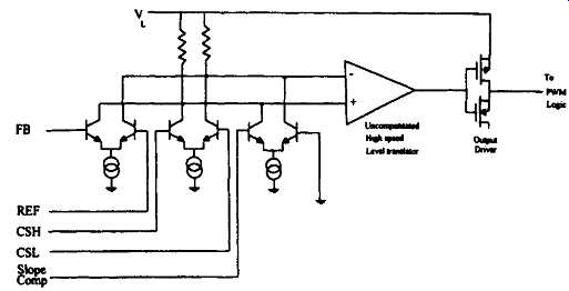
Above: Fig. 30 Block diagram of the main PWM comparator in the MAX 797
(Maxim Integrated Circuits Inc.)
6.3.3 Idle Mode Control Scheme
The MAX797's approach for conservation of battery power makes use of the SKIP input shown in Fig. 29. At light loads (SKIP = 0) the inductor current fails to exceed the 30 mV threshold set by the minimum current comparator. When this occurs, the minimum current comparator immediately resets the high-side latch at the beginning of the cycle unless the output voltage drops below the reference.
This sends the controller into a variable frequency idle mode, skipping most of the oscillator pulses, in order to cut back gate-charge losses.
Operation at a fixed frequency regardless of load conditions is however advantageous in terms of lowering PWM noise interference. Steps can be taken to remove the known emissions at a fixed frequencies. Therefore, a low-noise mode is enabled in the MAX 797 by making SKIP high. This forces fixed frequency operation by disabling the minimum current comparator.
6.3.4 Updated Voltage Mode Control
A newer solution by Linear Technology employs an advance voltage mode control scheme in its LTC 1430 controller. This controller, optimized for high power, 5V/3.xV applications operates at an efficiency greater than 90 percent in converter designs from 1A to greater than 50A output current. The LTC1430 uses a synchronous switching architecture with two N-channel output devices.
A block diagram of the LTC1430 is shown in Fig. 31. The primary control loop is a conventional voltage mode feedback loop. The load voltage is sensed across the output capacitor by the SENSE- and SENSE+ inputs, divided and fed to the feedback amplifier, where it’s compared to a 1.26V internal reference. The error signal is then compared to a saw tooth waveform from the oscillator to generate a pulse width modulated switching waveform.
Two other comparators in the feedback loop, MIN and MAX, provide high speed fault correction in situations where the feedback amplifier may not respond quickly enough. MIN compares the feedback signal to a voltage 40 mV (3 percent)
below the reference, and MAX compares it to a voltage 3 percent above the reference.
If the output falls below the minimum level, the MIN comparator overrides the feedback comparator and forces the loop to full duty cycle (about 90 percent). If the output rises above the 3 percent level, the MAX comparator forces the duty cycle to zero. These two comparators prevent extreme output perturbations in the presence of fast output transients. Additionally, it senses output current across the drain source resistance of the upper N-channel FET, providing an adjustable current limit without an external sense resistor.
6.3.5 A Master/Slave Architecture
Power Trends' solution (Travis 1996) is a master/slave architecture for DC/DC converter modules which allows the increase of available current in 3A steps. The designs show a 5V/3.3V converter with a 3A or 8A master coupled with three 3A slaves. The slaves add 9A of current to the master's current output. This approach is an attractive solution which leaves room for future system upgrades.
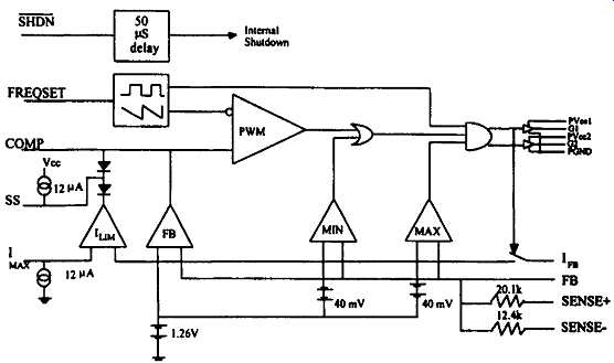
Above: Fig. 31 Block diagram of the LTCI430 Controller (Linear Technology
Corp)
6.3.6 Improved Process Technologies
Aiming at improved control loop bandwidth, Siliconix developed a high-speed CBiC/D (complementary bipolar/CMOS/DMOS) process which provides vertical pnp transistors with an ft of 2 GHz. The Si9145 voltage mode controller built with this technology has an error amplifier with a functional closed-loop bandwidth of 100kHz, helping to handle transient loads provided by today's microprocessors.
6.3.7 Switched Capacitor Converters
Switched capacitor (charge pump) converters use capacitors rather than inductors or transformers to store and transfer energy. The most compelling advantage of these converters is the absence of inductors. Compared with capacitors, inductors have greater component size, more EMI, greater layout sensitivity, and higher cost. Compared with other types of voltage converters, the switched capacitor converter can provide superior performance in applications that process low-level signals or require low noise operation.
Many capacitor-based voltage converters offer extremely low operating current--a useful feature in systems for which the load current is either uniformly low, or low most of the time. Thus, for small hand-held products, the light-load operating currents can be much more important than full-load efficiency in determining battery life. The basic operation of operation of switched capacitor voltage converters is shown in Fig. 32.
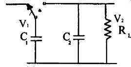
Above: Fig. 32 Principle of operation of switched capacitor converters
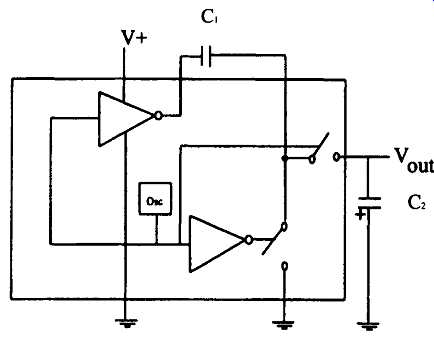
Above: Fig. 33 A simple IC switched capacitor implementation
When the switch is in the left position, C 1 charges to V 1. The total charge on C 1 is given by, ql = CIVI. When the switch moves to the fight position, C 1 discharges to V 2. The total charge on C 1 now is given by, q2 = Cll/2. the total charge transfer is given by,
If the switch is cycled at a frequency f, the charge transfer per second, or the current is given by,
... where R_eq is given by l/fC1.
The reservoir capacitor C 2 holds the output constant. The basic charge pump circuit can be modified for an inverted output by flipping C! in the internal switching arrangement. It can be used for doubling, tripling, or halving the input voltage with different external connections and by the use of external diodes. Fig. 33 shows a simple switched capacitor IC implementation with on-chip switches.
The usage of switched capacitor converters in laptop computers and small hand-held communications devices is increasing as their output current capabilities are increasing and the supply current required by the portable devices is decreasing.
Simple switched capacitor converters such as the MAX660 can generate 100mA at 3.3V when powered from a 2-cell battery of alkaline, NiCd or NiMH cells or a single primary lithium cell. A disadvantage of a circuit such as this is the lack of regulation. This is overcome by adding a regulator externally.
Internal regulation in monolithic switched capacitor converter chips is achieved either as linear regulation or as charge pump modulation. Linear regulation offers low output noise.
Charge pump modulation controls the switch resistance and offers more output current for a given cost or size because of the absence of a series-pass resistor.
Newer charge pump ICs employ an on-demand switching technique which enables low quiescent current and high output current capability at the same time. The simplicity of switched capacitor circuits, and hence its suitability for miniature equipment is amply illustrated in (Siliconix Inc. 1994), where the 8-pin Si7660 is used for voltage inversion, doubling and splitting.
6.3.8 SEPIC Converters
A relatively new converter architecture specially suited for battery operated equipment and battery charger applications is the SEPIC (Single Ended Primary Inductance Converter) topology. The SEPIC topology is shown in Fig. 34.
The two inductors L 1 and L 2 are often two identical windings on the same core. This topology is essentially similar to a 1" 1 transformer flyback converter, except for the addition of a capacitor C which forces identical AC voltages across the two inductors.
This is a step up/down topology with no inversion and no transformer.
However, the SEPIC topology provides DC isolation from the input to the output due to the presence of the capacitor.
The input/output relationship for this converter is given by:
This topology has the advantage of being operable over wide input voltage range. Due to this, this topology finds applications commonly in battery powered equipment and in battery chargers.
A converter design using the LT1373 current mode switching regulator with a SEPIC converter for generating 3.3V from a single Li-Ion battery are described in (Essaff 1995). In a typical application such as this, the battery voltage at full charge is above the output voltage, and when discharged it’s below the output voltage. This presents special difficulties in the converter design. The SEPIC architecture, with its wide input voltage range, is ideally suited for such applications.
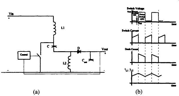
Above: Fig. 34 The SEPIC converter topology (a) The basic circuit (b)
Associated waveforms
The use of the SEPIC topology in battery charging is illustrated in an application in. This topology allows charging even when the input voltage is lower than the battery voltage. Further, it allows the current sense circuit to be ground-referred and completely separated from the battery itself, simplifying battery switching and system grounding problems.
The LT1512 is a constant current controller for SEPIC converters, for charging NiCd and NiMH batteries. It can also provide a constant voltage source for charging lithium ion batteries [39]. A special feature of this controller is an internal low-dropout regulator which provides a 2.3V supply for all internal circuitry, allowing input voltages to vary from 2.7V to 25V. This enables charging of batteries from varied sources such as wall adapters, car batteries and solar cells.
7 DC to DC Converter Applications and Its Uses
The modularity of design, the wide-ranging power supply requirements, and the need for compactness, portability, and expandability of today's electronic equipment all contribute to the numerous applications that DC to DC converters have found in modern electronic equipment.
7.1 DC to DC Converter Applications
The area in which DC to DC converters have found the widest application is in distributed power systems. A distributed power system is one which uses many small regulated power supplies, each located as close as possible to the load (Goodenough 1995). The bulk supply develops and distributes via a bus, an arbitrary voltage level. At appropriate points DC to DC converters change this voltage to the levels needed for the local circuitry.
A distributed power system can save space and reduce the weight of the system. It can also improve reliability and the quality of the generated power, and facilitate modular design and system expansion. Issues relating to distributed power systems are discussed in (Ormond 1990), (Goodenough 1995), (Ormond 1992). A typical application of a distributed power system is in telecommunication equipment. A relatively high voltage battery of 48 volts is located in the bottom of each electronic equipment rack. DC to DC converters are used on each rack card cage to step the voltage down to the required level. Another such application is in aircraft power distribution systems.
Modem electronic systems contain both analog and digital circuitry, where analog components require voltage levels such as 9, _+.12, and _+15. In mixed mode logic circuits, the conventional 5V supply as well as a 3.3 V supply for the latest low-power ICs are required. In such complex cases, DC to DC converters perform the valuable function of generating all required voltages while saving cost and space. A common application of 5 to 12 V converters is in flash memory programmers which require a supply of 12 V. Battery chargers that can be used off diverse power supplies ranging from the conventional mains supply to solar cells find the step-up/step-down ability of DC to DC converters a useful feature.
Another application area of DC to DC converters is in small, battery operated, portable equipment such as pagers, cameras, cellular phones, laptop computers, remote data acquisition and Instrumentation systems. The high efficiency and the small size of DC to DC converters become especially useful in such applications.
7.2 DC to DC Converter ICs
An increasing variety of chip-level DC to DC converters are appearing in the market. These devices are not only changing the way system designers structure their power supplies, but are also providing solutions to applications which previously required more costly, bulky and cumbersome approaches.
Integrated circuit DC to DC converters are available in a wide range of power and other capabilities. The lower power ICs can supply the exact voltage needed for a specific IC board, and higher power types can simplify the design by reducing the component count (Pryce 1988). The key parameters and capabilities of modem low-power DC to DC converters are described in this section using a representative sample from principal manufacturers such as Maxim, Datel, Linear Technology Corp., etc. For example, output power capabilities range from less than 1 W to more than 300W. Single, double, or triple output configurations are available.
Common output voltages are 3.3V, 5, 12, and 15 volts, while input voltages are quite varied. Common devices perform 5 to 12V, 9 to 12V, and 5 to 3.3 V conversions. Table 3-3 shows key features of some representative DC to DC converters.
Linear Technology Corp. produces a wide range of DC to DC converters, ranging from 0.5W micro-power devices to high efficiency 5A devices. Simple voltage doublers and dividers as well as circuits which can be used in many configurations are available. The LT1073, a gated oscillator mode IC, can operate from a supply of 1 V, and is typically used to generate 5 or 12 V from a single cell.
The XWR ( Wide Input Range) Series by Datel Inc. are high efficiency current mode converters, which have typical efficiencies of about 85 percent. Typical applications of these are in telecommunications, automotive, avionic, and marine equipment, and in portable battery operated systems. In addition to the XWR series, Datel also has the LP series of converters having 3W, 4.5W, 5W, and 10W outputs.
Maxim Integrated Products have also developed a wide variety of DC to DC converters, operating in current mode and resonant mode. The MAX632 is a typical low power device, which can operate from an input voltage of 5V to produce a 12 V output. This type of converters is ideal for powering low power analog circuits from a 5V digital bus. They are relatively inexpensive and require very few external components.
The LM3578 from National Semiconductors is a low/medium power converter which can be used in buck, boost, and buck-boost configurations. This can supply output currents as high as 750 mA. Siliconix's Si9100 and Si9102 can handle high input voltages. These chips are typically used in transformer coupled flyback and forward converter applications such as ISDN and PABX equipment and modems. Due to their high input voltage ratings, the Si9100 can operate directly from the -48V telephone line supply and the Si9102 from the -96 V double-battery telecom power supplies.
Further details of the above ICs as well as other similar products, application notes, etc., are found in (Linear Technology Corp. 1990)--(Essaff 1995). 3.8 State of the Art and Future Directions
As with all electronic disciplines, power supplies continue to get smaller, faster, better, and cheaper. The new techniques discussed in this section which extend the basic principles of DC/DC conversion give a taste of the future trends in power supply design and the driving forces behind them.
The adoption of progressively lower system voltages with progressively higher power in microprocessors drive DC/DC converter design in one direction, while battery operated systems provide another set of challenges. To face these challenges, and remain competitive in the market, key power supply designers continue to enhance their products using new material, new process technologies and new converter architectures.
TABLE 3 Some Representative DC to DC Converter ICs
Manufacturer | Model | Output Power (W)/Output Current (A ) | Output Voltage tv) Input Voltage (V)
- Linear Technology Corp.
- Datel Inc.
- Maxim Integrated Products Siliconix Inc.
- National Semiconductors Lambda Vicor Raytheon